A full degree-of-freedom photonic crystal spatial light modulator
Abstract
Harnessing the full complexity of optical fields requires complete control of all degrees-of-freedom within a region of space and time — an open goal for present-day spatial light modulators (SLMs), active metasurfaces, and optical phased arrays. Here, we solve this challenge with a programmable photonic crystal cavity array enabled by four key advances: (i) near-unity vertical coupling to high-finesse microcavities through inverse design, (ii) scalable fabrication by optimized, 300 mm full-wafer processing, (iii) picometer-precision resonance alignment using automated, closed-loop “holographic trimming”, and (iv) out-of-plane cavity control via a high-speed LED array. Combining each, we demonstrate near-complete spatiotemporal control of a 64-resonator, two-dimensional SLM with nanosecond- and femtojoule-order switching. Simultaneously operating wavelength-scale modes near the space- and time-bandwidth limits, this work opens a new regime of programmability at the fundamental limits of multimode optical control.
I Introduction
Programmable optical transformations are of fundamental importance across science and engineering, from adaptive optics in astronomy [1] and neuroscience [2, 3, 4], to dynamic matrix operations in machine learning accelerators [5] and quantum computing [6, 7, 8]. Despite this importance, fast, energy-efficient, and compact manipulation of multimode optical systems — the core objective of spatial light modulators (SLMs) — remains an open challenge [9, 10]. Specifically, the limited modulation bandwidth and/or pixel density of liquid crystal (LC) SLMs, digital micromirror displays, and other two-dimensional (2D) modulator arrays prevents complete control over the optical fields they tune.
Figure 1a illustrates these limitations for a typical SLM comprised of a two-dimensional (2D), -pitch array of tunable pixels (subscript ) emitting at wavelength into the solid angle with a system (subscript ) modulation bandwidth . Given these parameters, each “spatiotemporal” degree-of-freedom (DoF) simultaneously satisfying the minimum-uncertainty space- and time-bandwidth relations ( and , respectively) can be illustrated as a real-space voxel with area and time duration for pixel bandwidth . The optical-delay-limited pixel bandwidth can be approximated as a function of the achievable permittivity swing (for the speed of light ) using first-order perturbation theory [11] or similarly derived from linear scattering theorems [12].
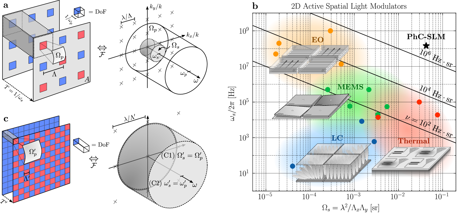
Integrating over the switching interval and aperture area then gives the total DoF count [27] 111Note that the exact coefficient of proportionality in Eqn. 1 depends on the number of polarizations, the complex amplitude and phase controllability of each mode, and the exact definition of distinguishability when defining the Fourier uncertainty relations. For simplicity, we have omitted these coefficients.
| (1) |
By comparison, the same switching period contains controllable modes, each confined to the pixel area and time window (shaded box in Fig. 1a). Complete spatiotemporal control with is only achieved under the following criteria: (C1) emitters fully “fill” the near-field aperture such that matches the field-of-view of a single array diffraction order; and (C2) . In the Fourier domain, the system’s “spatiotemporal bandwidth” counts the controllable DoF per unit area and time within a single far-field diffraction order. As illustrated by the shaded pillbox in Fig. 1a, (C1) and (C2) are both satisfied when matches the accessible pixel bandwidth .
Practical constraints have prevented present-day SLM technology from achieving this bound. In general, commercial devices approximate (C1) without achieving (C2). Specifically, they offer excellent near-field fill-factor across megapixel-scale apertures but use large , slow index perturbations. Liquid crystal SLMs, for example, are limited to by the slow rotation of viscous, anisotropic molecules that modulate the medium’s phase delay [29, 30]. Digital micromirror-based SLMs offer moderately faster ( Hz) binary amplitude modulation by displacing a mechanical reflector, but at the expense of diffraction efficiency [31]. Mechanical phase shifters [32, 33, 19, 20, 34] improve this efficiency but still require design trade-offs between pixel size and response time.
Recent research has focused on surmounting the speed limitations of commercial SLMs with integrated photonic phased arrays [16, 35, 36, 37] and active metasurfaces comprised of thermally [38, 39, 40], mechanically [41, 20], or electrically [25, 42, 43, 44, 26] actuated elements. These devices, however, do not satisfy (C1) (Table A2). Silicon photonics in particular has attracted significant interest due to its fabrication scalability; however, the combination of standard routing waveguides, high-power ( mW/ phase shift) thermal phase shifters, and vertical grating couplers in each pixel reduces the fill-factor of emitters, yielding [16]. Scattering into the numerous diffraction orders within then reduces the achievable zero-order and overall diffraction efficiencies ( and , respectively). For this reason, is a useful measure of near-field fill.
Various workarounds, including 1D phased arrays with transverse wavelength tunability [35, 45, 46], sparse antenna arrays [15], and switched arrays [47, 22] improve steering performance but restrict the spatiotemporal basis (i.e. limit ). Alternative nanophotonics-based approaches, often limited to 1D modulation, have their drawbacks as well: phase change materials [38, 39, 40] have slow crystallization rates and large switching energies, while electro-optic devices [48, 23, 25, 43, 44, 26, 49], to date, have primarily relied on large-area grating-based resonators to achieve appreciable modulation.
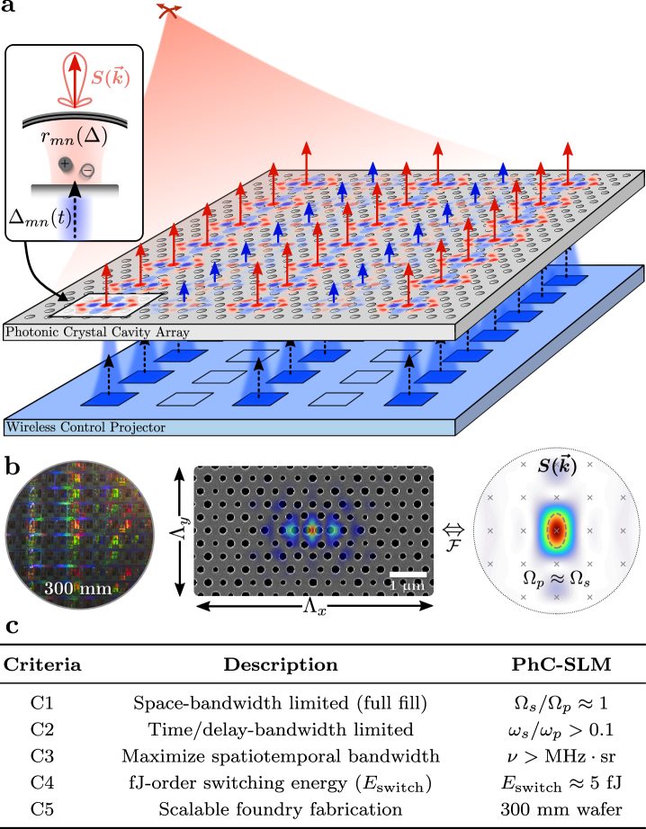
Figure 1b compares the performance of these and other experimentally-demonstrated, active, 2D SLMs as a function spatiotemporal bandwidth’s two components: modulation bandwidth and field-of-view . Controllability aside, the evident trade-off between these parameters illustrates the difficulty of creating fast, compact modulator arrays with high . Thus, in addition to satisfying the complete control criteria (C1) and (C2), an “ideal” SLM would (Fig. 2c): (C3) maximize by combining wavelength-scale pitches (for full-field beamforming) with gigahertz (GHz)-order bandwidths competitive with electronic processors; (C4) support femtojoule (fJ)-order switching energies as desired for information processing applications [51]; and (C5) have scalability to state-of-the-art megapixel-scale apertures.
These criteria motivate the resonant architecture in Fig. 1c. Here, (C3) and (C4) are achieved by switching a fully-filled array of wavelength-scale resonant optical antennas with fast, fJ-order perturbations . Each resonator’s far-field scattering and quality factor can then be tuned to achieve (C1) and (C2), respectively. Combined, this resonant SLM architecture enables complete, efficient control of the large spatiotemporal bandwidth supported by its constituent pixels.
Figure 2 illustrates our specific implementation of this full-DoF resonant SLM: the photonic crystal spatial light modulator (PhC-SLM) [52]. Coherent signal light is reflected off a semiconductor slab (permittivity ) hosting a 2D array of semiconductor PhC cavities with instantaneous resonant frequency . A short-wavelength incoherent control plane imaged onto the cavity array controls each resonator’s detuning via the permittivity change induced by photo-excited free carriers [53, 54]. We optimize the resonator bandwidth (corresponding to a quality factor ) to maximize the linewidth-normalized detuning without significantly attenuating the cavity’s response at the carrier lifetime ()-limited modulation rate . Under these conditions, free carrier dispersion efficiently modulates the complex cavity reflectivity to enable fast ( MHz given a ns free carrier lifetime [55]), low-energy (fJ-order) conversion of incoherent control light into a dense array of coherent, modulated signal modes (Appendix A).
This out-of-plane, all-optical switching approach is motivated by the recent development of high-speed, high-brightness LED arrays [56, 57] integrated with complementary metal-oxide-semiconductor (CMOS) drive electronics for consumer displays [58, 59] and high-speed visible light communication [60, 61]. In particular, gallium nitride LED arrays with GHz-order modulation bandwidths [61, 62], sub-micron pixel pitches [63], and large pixel counts [64] have been demonstrated within the past few years. Applying these arrays for reconfigurable, “wireless” all-optical cavity control eliminates electronic tuning elements at each pixel to avoid optical loss, pixel pitch limitations, and interconnect bottlenecks for planar architectures (as aperture area grows, pixel controls eventually cannot be routed through the perimeter) [65].
Free of these constraints, we designed high-finesse, vertically-coupled microcavities offering coupling efficiencies , phase-dominant reflection spectra [17, 66], and directional emission for high-efficiency beamforming (Section II). Bespoke, wafer-scale processing allows us to fabricate these “resonant antennas” in arrays with mean quality factors and sub-nm resonant wavelength standard deviation (Section III). For fine tuning, we developed a parallel laser-assisted thermal oxidation [67, 68] protocol to then trim cavity arrays to picometer-order uniformity [67, 68] (Section IV), enabling high-speed spatial light modulation with fJ-order switching energies and MHz (Section V). Compared to the previous devices surveyed in Fig. 1b, our PhC-SLM offers near-complete control over an order-of-magnitude larger spatiotemporal bandwidth.
II Inverse-Designed Resonant Pixels
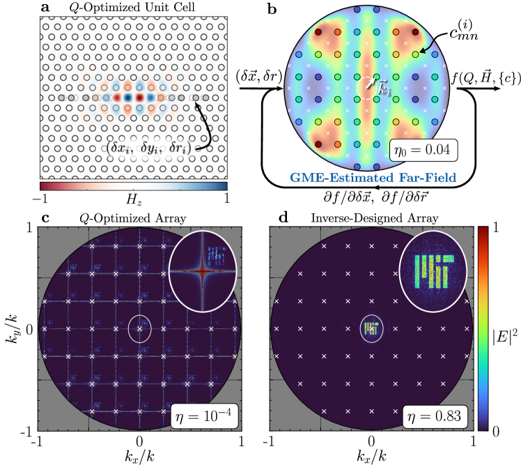
The sub-wavelength (i.e. normalized volume relative to a cubic wavelength in the confining dielectric of refractive index ), high- (up to ) [69, 70] modes of 2D PhC cavities enable (C4) [71], but at the expense of (C1) since optimization (via hole displacements as in Fig. 3a [72]) cancels radiative leakage. The exact displacement parameters are typically numerically optimized in computationally expensive finite-difference time-domain (FDTD) simulations, which ultimately limits the number of free parameters. Compared to the ideal apertures in Fig. 1c, the optimized cavity unit cell confines a spatially complex mode with (Fig. 4b, background), violating (C1) and limiting the zero-order diffraction efficiency to . The result is poor beamforming performance as exemplified by the distorted, low-efficiency far-field pattern emitted by a cavity array with optimized detunings (derived with the algorithm in Appendix F) to match a target far-field image (MIT logo).
Fortunately, these limitations are not fundamental: the effective scattering aperture of a resonant mode can extend beyond its decay area . This apparent space-bandwidth violation is enabled by resonant scattering from the mode’s evanescent field, which raises the basic question: how should scatterers be arranged to produce a desired far-field emission pattern?
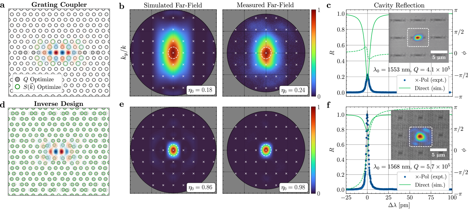
One established approach is a harmonic -period grating perturbation (Fig. 4a) that “folds” energy concentrated at the band-edge back to , yielding vertical radiation at the expense of reduced [73, 74, 75, 76]. In the perturbative regime, the far-field scattering profile is an image of the broad band-edge mode. Thus, once the grating-induced loss becomes dominant, further magnifying the perturbation reduces without significantly improving directivity. Fig. 4b shows the narrowed far-field profile produced by a grating perturbation, which balances the reduced and a modest diffraction efficiency improvement ().
By contrast, our design strategy (Fig. 3b) combines semi-analytic guided mode expansion (GME) simulations with automatic differentiation to maximize (and thereby the effective near-field fill factor) for a given target using all of the hole parameters. In each iteration, GME approximates the cavity eigenmode and radiative loss rates at each of the array’s reciprocal lattice vectors (i.e. diffraction orders) offset by the Bloch periodic boundary conditions [77]. These coupling coefficients coarsely sample the cavity’s approximate far-field emission (Appendix C). Scanning over the irreducible Brillouin zone of the rectangular cavity array improves the sampling resolution, and an overall can be estimated by averaging the total loss rates in each simulation. Reverse-mode automatic differentiation then allows us to efficiently optimize an objective function
| (2) |
targeting three main goals: 1) increase to a design value ; 2) force the associated radiative loss into the array’s zeroth diffraction order for efficient vertical coupling; and 3) minimize by maximizing , the electric-field magnitude at the center of the unit cell. The resulting designs support tunable- resonances with near-diffraction-limited () vertical beaming comparable to the ideal planar apertures of Fig. 1c. The example design of Fig. 4d, for instance, maintains with based on the simulated far-field profile in Fig. 4e.
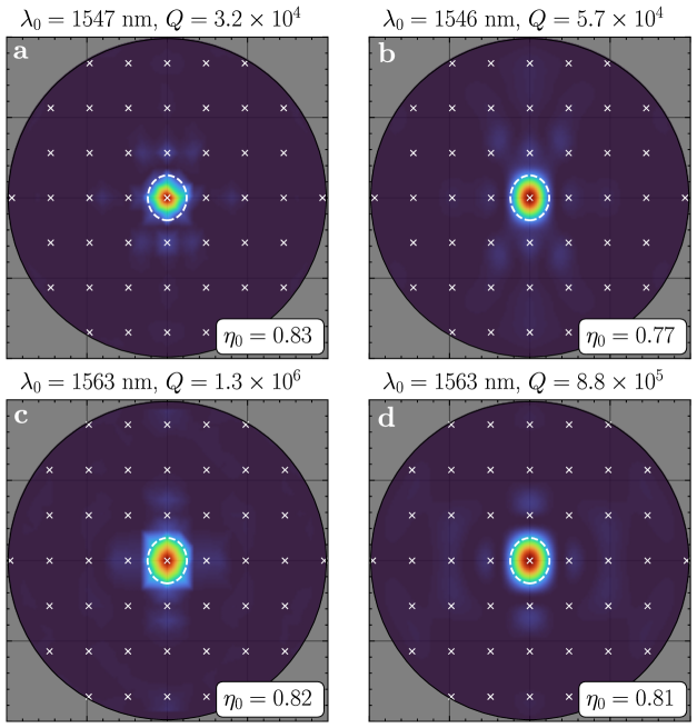
We prototyped each design at a commercial electron beam lithography (EBL) foundry 222Applied Nanotools, Inc. https://www.appliednt.com/ before transitioning to the wafer-scale foundry process described in Sec. III. The near- and far-field reflection characteristics of the fabricated devices were measured with the cross-polarized microscopy setup detailed in Appendix D. Fig. 4b-c and Fig. 4e-f show the results for the grating coupled and inverse-designed cavities, respectively. The optimal grating-coupled cavities offer at with a near-field resonant scattering profile well-centered on the cavity defect (Fig. 4c, inset). The mode mismatch between this wavelength-scale PhC mode and the wide-field input beam (Gaussian beam with waist diameter for array-level excitation) is further evidenced by the small normalized reflection amplitude (relative to that of the inverse designed cavities) on resonance as well as the broad far-field profile (Fig. 4b) with .
By comparison, inverse design non-perturbatively modifies the cavity mode (Fig. 4d) to produce the near-ideal measured far-field profile in Fig. 4e satisfying (C1) with while simultaneously increasing to . We attribute the slight increase in zero-order diffraction efficiency over the simulated value to the substrate-dependent effects described in Appendix G. The fully-filled near-field resonant scattering image in Fig. 4f explains the close resemblance between this measured and that of an ideal uniform aperture [79]. In addition, the narrowed emission profile yields a increase in cross-polarized reflection and the phase-dominant simulated direct reflection spectrum in Fig. 4f. The latter is achieved by 94% one-sided coupling to a Gaussian beam with optimized waist diameter (Appendix E).
Combined, these results break the traditional coupling– tradeoff (offering an order-of-magnitude improvement in the figure-of-merit for the prototype devices in Fig. 4) to enable high-performance beamforming at the space-bandwidth limit (C1). These results are supported by the simulated hologram in Fig. 3d: an array of optimally detuned, inverse-designed cavities forms a clear far-field image with a several order-of-magnitude improvement in overall diffraction efficiency () over existing designs.
III Foundry-Fabricated High-Finesse Microcavity Arrays
While EBL enables fabrication of few-pixel prototypes with state-of-the-art resolution and accuracy, serial direct-write techniques do not satisfy (C5). Field stitching issues and sample preparation aside, a single cm2, megapixel-scale sample would require a full day of EBL write time alone. We therefore developed a full-wafer deep-ultraviolet photolithography process specifically optimized for wavelength-pitch arrays of high- PhC microcavities in a commercial foundry [80].
A central goal was to create vertical etch side-walls. The transmission electron microscope (TEM) cross-section in Fig. 5i shows that the default fabrication process (optimized for isolated waveguides) yielded an oblique (), incomplete etch through the silicon device layer for the target PhC lattice parameters. Both nonidealities erase the membrane’s vertical reflection symmetry, leading to coupling between even- and odd- symmetry (about the slab midplane) modes that ultimately limits the achievable of bandgap-confined resonances [81]. By contrast, our revised fabrication process achieves near-vertical sidewall angles (Fig. 5ii), yielding high-quality PhC lattices for a range of hole diameters between the nm critical-dimension and (Fig. 5c). Using TEM cross-sectioning and automated optical metrology as feedback over multiple 300 mm wafer runs in the AIM Photonics foundry’s 193 nm DUV water-immersion lithography line, this new process relies on a combination of dose-optimized reverse (positive) tone lithography, high-accuracy laser written masks, and optimized etch termination. Following fabrication and dicing, we post-processed individual die with a backside silicon nitride anti-reflection coating and, as required, suspend the PhC membranes with a timed wet etch.
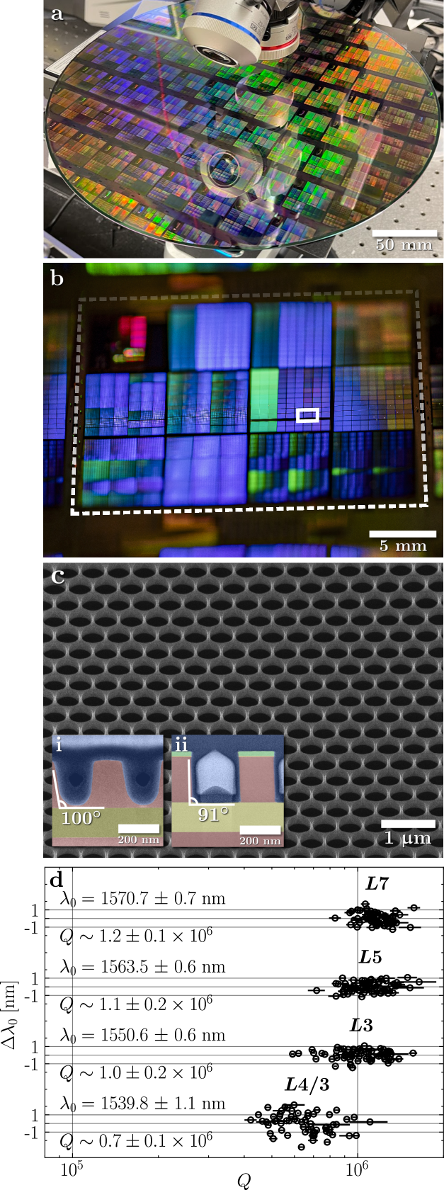
The resulting die contain isolated and arrayed PhC cavities with swept dimensions to offset systematic fabrication biases. We chose -type cavity designs — formed by removing holes from the PhC lattice as demonstrated by the unit cells in Fig. 4 — to host tunable-volume (via variable ), high- resonant modes with even reflection symmetry (about the unit cell axes) as required for vertical emission [82]. The highest-performance isolated devices feature with normalized volumes . With a joint spectral- and spatial-confinement (quantified by the figure-of-merit , these devices are among the highest-finesse optical cavities ever fabricated in a foundry process.
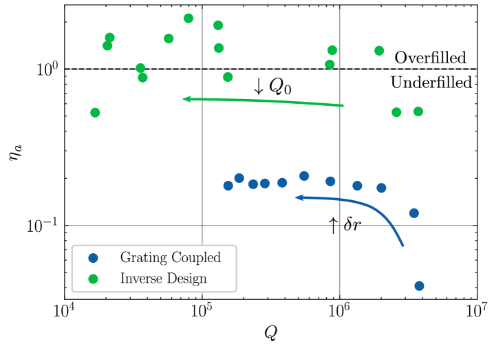
Our optimized foundry processing extends this exceptional single-device performance (rivaling record EBL-fabricated devices) to large-scale cavity arrays. We developed a fully-automated measurement system (Appendix D) to locate and characterize hundreds of cavities per second via parallel camera readout. The resulting data, extracted from over devices measured across the wafer, allow us to statistically analyze resonator performance and fabrication variability at the die, reticle, and wafer level. Fig. 5d, for example, shows resonant wavelength and variations within arrays of four different cavity designs. Using camera readout of the reflected wide-field excitation, each data set is extracted from a single wavelength scan of a tunable laser. Besides the expected correlation between uniformity and mode volume [83], the data demonstrates — for the first time, to our knowledge — the ability to fabricate sub-wavelength () microcavity arrays with and sub-nanometer resonant wavelength standard deviation ( nm). Critically for beamforming, this uniformity also extends to the far-field: Appendix H shows that each cavity in an array emits vertically with , in quantitative agreement with the simulated result in Fig. 4.
IV Holographic Trimming
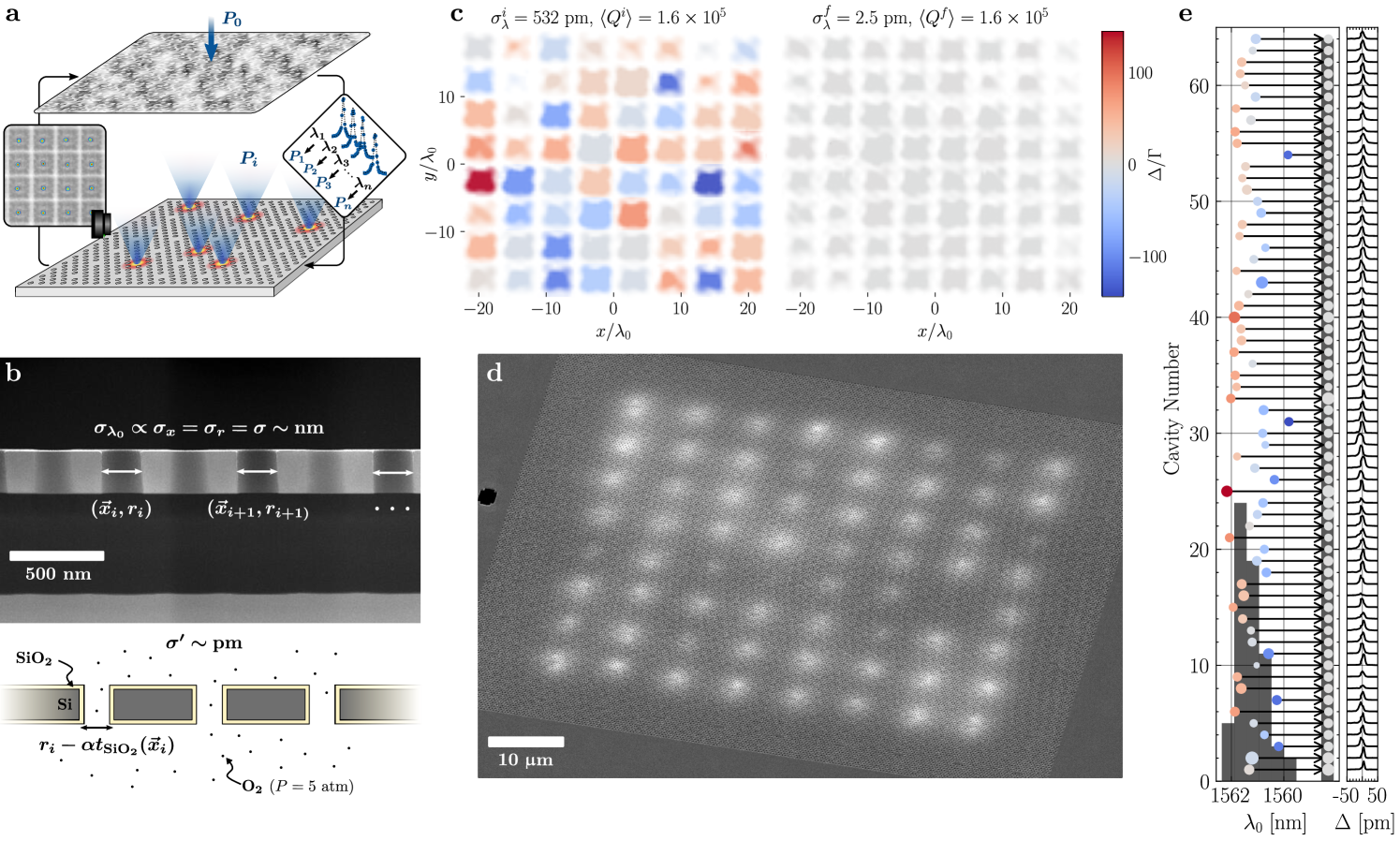
In addition to these overlapping far-field emission profiles, programmable multimode interference requires each cavity to operate near a common resonant wavelength . For sufficiently high- resonators, this tolerance cannot be solely achieved through optimized fabrication since fabrication fluctuations translate to resonant wavelength variations [84, 85]. Our prototype arrays of cavities (chosen to optimally balance requirements on , , directive emission, and fabrication tolerance) typically span a peak-to-peak wavelength variation (given nm), corresponding to hundreds of linewidths for the target .
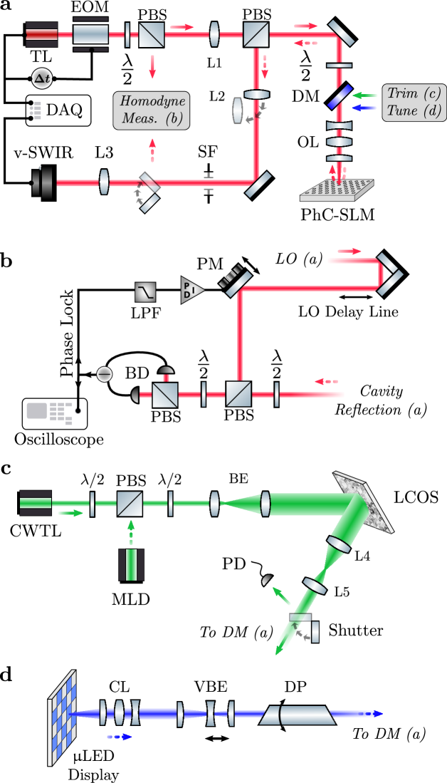
To correct this nonuniformity, we developed an automated, low-loss, and picometer-precision trimming procedure based on laser-assisted thermal oxidation (Fig. 6). Two features of our approach resolve the speed and controllability limitations of prior single-device implementations [67, 68]: 1) accelerated oxidation in a high-pressure chamber with in-situ characterization; and 2) holographic fanout of the trimming laser to simultaneously address multiple devices. In each iteration of the automated trimming loop (Fig. 6a), the resonant wavelengths are measured and a subset containing devices is selected to maximize the total trimming distance to a target wavelength . Each cavity in is then targeted by a visible laser distributed by the liquid crystal SLM setup described in Appendix D. To generate the required phase masks, we developed an open-source, GPU-accelerated experimental holography software package that implements fixed-phase, weighted Gerchberg-Saxton (GS) phase retrieval algorithms 333slm-suite. https://github.mit.edu/cpanuski/qp-slm. Using camera feedback, the algorithm can generate thousands of near-diffraction-limited foci with peak-to-peak power uniformity and single-camera-pixel-order location accuracy within a few iterations (Appendix I).
The holographically-targeted pixels are then laser-heated with a computed exposure power and duration (based on the current trimming rates, resonance locations, and other array characteristics) to grow thermal oxide at the membrane surface. For thin oxide layers, the consumption of silicon during the reaction with ambient oxygen permanently blueshifts the cavity resonance in proportion to the oxide thickness (Fig. 6b) [68]. Per the Deal-Grove model, the rate-limiting diffusion of oxygen through the grown oxide accelerates with increasing oxygen pressure — a well-known technique in microelectronics fabrication [87]. We therefore oxidize our samples in pure oxygen with partial pressure , enabling resonance trimming rates over wavelength ranges. After each trimming exposure, we remeasure the resonance statistics and recycle the loop until all devices are aligned within a set tolerance about . The trimming algorithm also accounts for long-term moisture adsorption to the membrane surface, thermal cross-talk, and trimming rate variations (Appendix J).
Fig. 6 demonstrates the results of this trimming procedure applied to our prototype pixel PhC-SLM. Prior to trimming, the hyperspectral near-field reflection image in Fig. 6c shows the large ( linewidths for the mean quality factor ) resonant wavelength variation between the otherwise spatially uniform and high-fill resonant modes. Holographic trimming reduces the wavelength standard deviation and peak-to-peak spread by to and , respectively, enabling all 64 devices (imaged in Fig. 6d) to be resonantly excited at a common operating wavelength (Fig. 6e). Since is directly related to the corresponding hole radius and placement variability ( and , respectively) with an design-dependent constant of proportionality, the thermal oxide homogenizes the effective dimensions of each microcavity to the picometer scale. The mean quality factor and near-field reflection profile of the array remain largely unmodified throughout the process as evidenced by Fig. 6c and Fig. 6e.
To our knowledge, these results are the first demonstration of parallel, in situ, non-volatile microcavity trimming. The achievable scale is currently limited by environmental factors that could be overcome with stricter process control (Appendix J). Even without these improvements, the current uniformity, scale, and induced loss outperform the corresponding metrics of the previous techniques reviewed in Appendix J, paving the way towards scalable integrated photonics with high- resonators.
V All-Optical Spatial Light Modulation
Once trimmed to within a linewidth, each resonator reflects an incident coherent field , producing a far-field output [88]
| (3) |
that can be dynamically controlled within by setting the detuning (and therefore the near-field reflection coefficient ) of each resonator. Experimentally, we measure the intensity pattern on the back focal plane of a microscope objective above the PhC-SLM (as with the single-device characterization in Sec. II) and optically program via photo-excited free carriers. The corresponding setups are detailed in Appendix D.
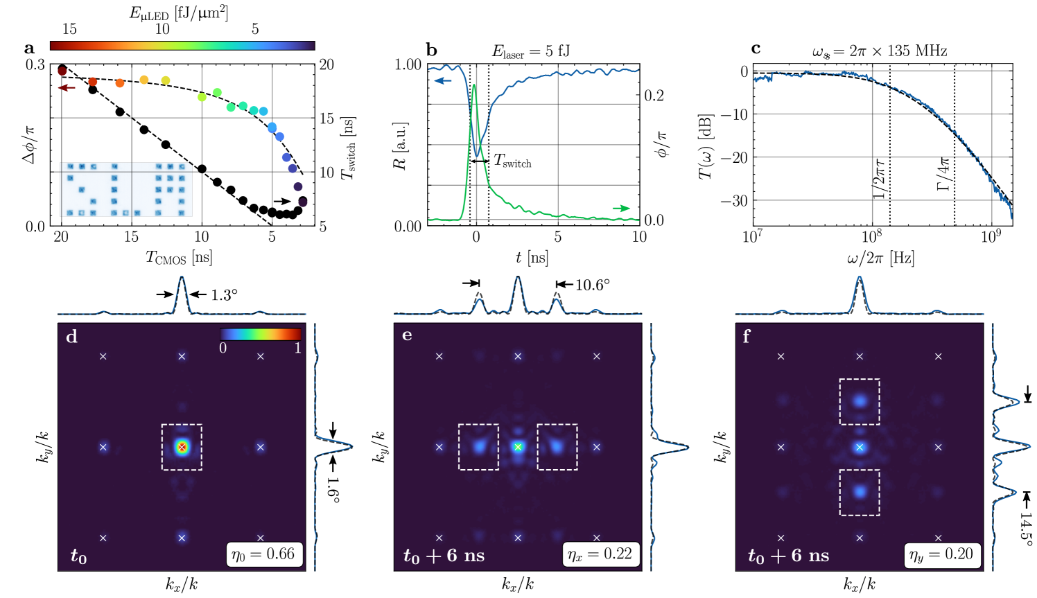
Absent a control input (), Fig. 7d shows the static far-field intensity pattern of a wide-field-illuminated (i.e. ) trimmed array with and pm at nm. The inverse-designed cavity unit cells minimize scattering into undesired diffraction orders, producing a high-efficiency () zero-order beam with the expected and horizontal and vertical beamwidths given the aperture size. The cross-sectional beam profiles are well matched to the simulated emission profile of uniform apertures with width , suggesting an 80% effective linear fill of the array. This extracted value agrees with the observed zero-order efficiency and the array’s physical design (each cavity offering near-unity fill was padded to to limit coupling to adjacent cells).
After confirming the static performance of the array, we conducted optical switching experiments with two sources: an incoherent LED array and a pulsed visible laser. The LED array contains individually-addressable gallium nitride LEDs with 150 MHz small-signal bandwidth and cd/m2 peak luminances (at 450 nm) flip-chip bonded to high-efficiency CMOS drivers [89, 60]. Using the setup in Appendix D, we imaged the 100 m-pitch array with variable demagnification and rotation onto the PhC cavity array. Digitally triggering the CMOS drivers then enables reconfigurable, binary optical addressing as illustrated by the imaged projections of three letters on the PhC-SLM (Fig. 7a). We measured the resulting pixel reflection amplitude and phase using locked, shot-noise-limited balanced homodyne detection (Appendix D). Fig. 7a depicts the maximum phase shift as a function of CMOS trigger duration and imaged pump energy density . Single-cavity switching is possible with energy densities below fJ/m2 (corresponding to fJ total energy for our chosen demagnification) and a minimum trigger duration ns. Shorter trigger pulses produce relatively constant-width pulses (due to the LED fall time) with insufficient energy for high-contrast switching.
Confining visible pump pulses in space and time to the silicon free-carrier diffusion length (m) and lifetime ( ns), respectively, would reduce the required switching energy and maximize bandwidth bandwidth. While either metric is achievable with existing LED arrays [90, 63] and optimization to achieve both simultaneously is ongoing [91], we demonstrated the expected performance enhancement with a pulsed visible ( nm) laser. Fig. 7b shows that 3 dB power reflectivity changes and high-contrast phase modulation are feasible for 5 fJ pump pulses over a switching interval ns, thereby satisfying (C4). Free-carrier dispersion is the dominant switching mechanism for these isolated, ns-order switching events (Appendix A). While repeated switching over s-order timescales leads to a slowly-varying thermo-optic detuning [92], various optical communications techniques (constant-duty line codes, for example [93]) can maintain average device temperature during high-speed free carrier modulation. To demonstrate this decoupling of switching mechanisms, we measured the normalized small-signal transfer function between a harmonic pump power (produced by a network analyzer-driven amplitude electro-optic modulator) and the phase-locked homodyne response. When aligned to the thermally-detuned resonance, the results (Fig. 7c) match the expected second-order response set by carrier- and cavity-lifetime-limited bandwidths ( for a fitted carrier lifetime ns and the measured GHz, respectively). While satisfying (C2) therefore requires higher- resonators, the current regime of operation enables near-complete control over a larger bandwidth , i.e. without significantly degrading the carrier-lifetime-limited modulation bandwidth.
Combining this optimized switching with the space-bandwidth-limited vertical beaming of each resonator enables multimode programmable optics approaching the fundamental limits of spatiotemporal control. We currently probe the PhC-SLM in a wide-field, cross-polarized setup that produces amplitude-dominant Lorentzian reflection profiles regardless of the resonator coupling regime (cavity emission is isolated from specular reflection). For simplicity, we therefore conducted proof-of-concept demonstrations using the PhC-SLM as an array of high-speed binary amplitude modulators. In this modality, a nanosecond-class pulsed visible laser is passively fanned out to the desired devices. Devices targeted by pump light are detuned far from resonance () and effectively extinguished, whereas unactuated cavities retain their high reflectivity.
We used pump-probe spectroscopy for wide-field imaging of these few-nanosecond switching events (Appendix D). Short infrared probe pulses were carved with a electro-optic amplitude modulator (DC biased to an intensity null) and variably delayed to coincide with the arrival of visible pump light at the PhC membrane, gating probe field transmission to the IR camera. We then measured the near- and far-field reflection as a function of the probe delay to reconstruct switching events with sub-nanosecond resolution. Fig. 7e-f plots the resulting far-field intensity profiles for horizontal and vertical on-off gratings. For a ns probe pulse width, the maximum near-field extinction of targeted cavities (7.4 dB and 9.8 dB for horizontal and vertical gratings, respectively) occurs within a ns delay; i.e. just after the pump and probe pulses completely overlap. This minimum probe pulse width is limited by the requirement for high imaging contrast between probe pulses and leakage (due to the imperfect probe modulator extinction) given the instrument-limited trigger repetition rate (MHz) and camera integration time.
As expected, the input field is primarily scattered into first-order diffraction peaks within the (greater than ) 2D field-of-view of . The illustrated cross sectional beam profiles again agree with analytic results for a 80% filled linear array of uniform apertures (black dashed lines). For the horizontal grating Fig. 7e, the fit is scaled by a factor of to account for the increased reflectivity of unactuated cavities during switching events, which we attribute to residual coupling between adjacent cavities. In both cases, the pattern diffraction efficiencies — measured as the fraction of integrated power within the outlined regions in Fig. 7 — compare favorably to the efficiency of the fitted uniform aperture array. Even with amplitude-dominant modulation, these metrics exceed the efficiencies of previous resonator-based experiments due to our high-directivity PhC antenna array [17].
VI Summary and Outlook
These proof-of-concept experiments demonstrate near-complete spatiotemporal control of a narrow-band optical field filtered in space and time by an array of wavelength-scale, high-speed resonant modulators. While the general resonant architecture (Fig. 1c) is applicable to a range of microcavity geometries and modulation schemes, the combination of our high-, vertically-coupled PhC cavities with efficient, all-optical free-carrier modulation achieves (C1-5) with an ultrahigh per-pixel spatiotemporal bandwidth . This MHz-order modulation bandwidth per aperture-limited spatial mode corresponds to a more than ten-fold improvement over the 2D spatial light modulators reviewed in Fig 1b. Our wafer-scale fabrication and parallel trimming offer a direct route towards scaling this performance to spectrally-multiplexed, apertures for exascale interconnects beyond the reach of current electronic systems, thus motivating the continued development of optical addressing and control techniques.
The PhC-SLM opens the door to a number of applications and opportunities, including: high-definition, high-frame-rate holographic displays by the integration of a back-reflector (see Appendices E-G) for one-sided, phase-only, and full-DoF spatiotemporal modulation; compact device integration via direct transfer printing of our cavity arrays onto a high-bandwidth LED array [94]; three-dimensional optical addressing and imaging by combining on-demand LED control with statically trimmed detuning profiles that continuously steer pre-programmed patterns [95]; large-scale programmable unitary transformations for universal linear optics processors [96]; focal plane array sensors for high-spatial-resolution readout of refractive index perturbations in imaging applications from endoscopy to bolometry and quantum-limited superresolution [97, 98, 99]; optical neural network acceleration via low-power, high-density unitary transformation of free-space optical inputs [5, 100]; and high-speed adaptive optics enabling free-space compressive sensing, deep-brain neural stimulation, and real-time scattering matrix inversion in complex media [101, 102]. Moreover, whereas we have so far considered only mode transformations, the PhC-SLM’s high- resonant enhancement suggests the possibility of programming the quantum optical excitations/fields of these modes for applications ranging from multimode squeezed light generation [103], to multiplexed single photon sources for linear optics quantum computing [6, 104] or deterministic photonic logic [105, 106].
Acknowledgements.
The authors thank Flexcompute, Inc. for supporting FDTD simulations, the MIT.nano staff for fabrication assistance, and M. ElKabbash (MIT) for useful discussions. C.P. was supported by the Hertz Foundation Elizabeth and Stephen Fantone Family Fellowship. S.T.M. is funded by the Schmidt Postdoctoral Award and the Israeli Vatat Scholarship. Experiments were supported in part by Army Research Office grant W911NF-20-1-0084, supervised by M. Gerhold, the Engineering and Physical Sciences Research Council (EP/M01326X/1, EP/T00097X/1), and the Royal Academy of Engineering (Research Chairs and Senior Research Fellowships). This material is based on research sponsored by Air Force Research Laboratory under agreement number FA8650-21-2-1000. The U.S. Government is authorized to reproduce and distribute reprints for Governmental purposes notwithstanding any copyright notation thereon. The views and conclusions contained herein are those of the authors and should not be interpreted as necessarily representing the official policies or endorsements, either expressed or implied, of the United States Air Force, the Air Force Research Laboratory or the U.S. Government. C.P. and D.E. conceived the idea, developed the theory, and led the research. M.M. and C.P. developed the far-field optimization technique and designs. C.B. developed the optimized resonator detuning theory. C.P. conducted the experiments with assistance from I.C. (trimming experiments), S.T.M. (holography software), and A.G. (LED measurements). J.J.M., M.D., and M.S. contributed the LED arrays and guided the incoherent switching experiments. C.H. and J.W.B. fabricated the initial samples for evaluation prior to foundry process development by C.T., J.S.L., J.M., and G.L. S.P. assisted with wafer post-processing. M.F. coordinated and led the foundry fabrication with assistance from G.L. and D.C. C.P. wrote the manuscript with input from all authors.References
- Gardner et al. [2006] J. P. Gardner, J. C. Mather, M. Clampin, R. Doyon, M. A. Greenhouse, H. B. Hammel, J. B. Hutchings, P. Jakobsen, S. J. Lilly, K. S. Long, J. I. Lunine, M. J. Mccaughrean, M. Mountain, J. Nella, G. H. Rieke, M. J. Rieke, H.-W. Rix, E. P. Smith, G. Sonneborn, M. Stiavelli, H. S. Stockman, R. A. Windhorst, and G. S. Wright, The James Webb Space Telescope, Space Science Reviews 123, 485 (2006).
- Packer et al. [2013] A. M. Packer, B. Roska, and M. Häusser, Targeting neurons and photons for optogenetics, Nature neuroscience 16, 805 (2013).
- Marshel et al. [2019] J. H. Marshel, Y. S. Kim, T. A. Machado, S. Quirin, B. Benson, J. Kadmon, C. Raja, A. Chibukhchyan, C. Ramakrishnan, M. Inoue, J. C. Shane, D. J. McKnight, S. Yoshizawa, H. E. Kato, S. Ganguli, and K. Deisseroth, Cortical layer–specific critical dynamics triggering perception, Science 365, eaaw5202 (2019).
- Demas et al. [2021] J. Demas, J. Manley, F. Tejera, K. Barber, H. Kim, F. M. Traub, B. Chen, and A. Vaziri, High-speed, cortex-wide volumetric recording of neuroactivity at cellular resolution using light beads microscopy, Nature Methods 18, 1103 (2021).
- Hamerly et al. [2019] R. Hamerly, L. Bernstein, A. Sludds, M. Soljačić, and D. Englund, Large-scale optical neural networks based on photoelectric multiplication, Physical Review X 9, 021032 (2019).
- Kok et al. [2007] P. Kok, W. J. Munro, K. Nemoto, T. C. Ralph, J. P. Dowling, and G. J. Milburn, Linear optical quantum computing with photonic qubits, Reviews of modern physics 79, 135 (2007).
- Barredo et al. [2018] D. Barredo, V. Lienhard, S. De Leseleuc, T. Lahaye, and A. Browaeys, Synthetic three-dimensional atomic structures assembled atom by atom, Nature 561, 79 (2018).
- Ebadi et al. [2021] S. Ebadi, T. T. Wang, H. Levine, A. Keesling, G. Semeghini, A. Omran, D. Bluvstein, R. Samajdar, H. Pichler, W. W. Ho, S. Choi, S. Sachdev, M. Greiner, V. Vuletić, and M. D. Lukin, Quantum phases of matter on a 256-atom programmable quantum simulator, Nature 595, 227 (2021).
- Shaltout et al. [2019a] A. M. Shaltout, V. M. Shalaev, and M. L. Brongersma, Spatiotemporal light control with active metasurfaces, Science 364, eaat3100 (2019a).
- Piccardo et al. [2021] M. Piccardo et al., Roadmap on multimode light shaping, Journal of Optics 24, 013001 (2021).
- Joannopoulos et al. [2011] J. D. Joannopoulos, S. G. Johnson, and J. N. Winn, Photonic Crystals: Molding the Flow of Light - Second Edition (Princeton, 2011).
- Miller [2007] D. A. Miller, Fundamental limit to linear one-dimensional slow light structures, Physical review letters 99, 203903 (2007).
- McKnight et al. [1994] D. J. McKnight, K. M. Johnson, and R. A. Serati, 256 256 liquid-crystal-on-silicon spatial light modulator, Applied Optics 33, 2775 (1994).
- Li et al. [2020] J. Li, P. Yu, S. Zhang, and N. Liu, Electrically-controlled digital metasurface device for light projection displays, Nature communications 11, 1 (2020).
- Fatemi et al. [2019] R. Fatemi, A. Khachaturian, and A. Hajimiri, A nonuniform sparse 2D large-FOV optical phased array with a low-power PWM drive, IEEE Journal of Solid-State Circuits 54, 1200 (2019).
- Sun et al. [2013] J. Sun, E. Timurdogan, A. Yaacobi, E. S. Hosseini, and M. R. Watts, Large-scale nanophotonic phased array, Nature 493, 195 (2013).
- Horie et al. [2017] Y. Horie, A. Arbabi, E. Arbabi, S. M. Kamali, and A. Faraon, High-speed, phase-dominant spatial light modulation with silicon-based active resonant antennas, Acs Photonics 5, 1711 (2017).
- Shrauger and Warde [2001] V. Shrauger and C. Warde, Development of a high-speed high-fill-factor phase-only spatial light modulator, in Diffractive and Holographic Technologies for Integrated Photonic Systems, Vol. 4291 (International Society for Optics and Photonics, 2001) pp. 101–108.
- Yang et al. [2014] W. Yang, T. Sun, Y. Rao, M. Megens, T. Chan, B.-W. Yoo, D. A. Horsley, M. C. Wu, and C. J. Chang-Hasnain, High speed optical phased array using high contrast grating all-pass filters, Optics express 22, 20038 (2014).
- Wang et al. [2019] Y. Wang, G. Zhou, X. Zhang, K. Kwon, P.-A. Blanche, N. Triesault, K.-s. Yu, and M. C. Wu, 2D broadband beamsteering with large-scale MEMS optical phased array, Optica 6, 557 (2019).
- Bartlett et al. [2019] T. A. Bartlett, W. C. McDonald, and J. N. Hall, Adapting Texas Instruments DLP technology to demonstrate a phase spatial light modulator, in Emerging Digital Micromirror Device Based Systems and Applications XI, Vol. 10932 (International Society for Optics and Photonics, 2019) p. 109320S.
- Zhang et al. [2022] X. Zhang, K. Kwon, J. Henriksson, J. Luo, and M. C. Wu, A large-scale microelectromechanical-systems-based silicon photonics LiDAR, Nature 603, 253 (2022).
- Shuai et al. [2017] Y.-C. Shuai, D. Zhao, Y. Liu, C. Stambaugh, J. Lawall, and W. Zhou, Coupled bilayer photonic crystal slab electro-optic spatial light modulators, IEEE Photonics Journal 9, 1 (2017).
- Junique et al. [2005] S. Junique, Q. Wang, S. Almqvist, J. Guo, H. Martijn, B. Noharet, and J. Y. Andersson, GaAs-based multiple-quantum-well spatial light modulators fabricated by a wafer-scale process, Applied optics 44, 1635 (2005).
- Smolyaninov et al. [2019] A. Smolyaninov, A. El Amili, F. Vallini, S. Pappert, and Y. Fainman, Programmable plasmonic phase modulation of free-space wavefronts at gigahertz rates, Nature Photonics 13, 431 (2019).
- Benea-Chelmus et al. [2021] I.-C. Benea-Chelmus, M. L. Meretska, D. L. Elder, M. Tamagnone, L. R. Dalton, and F. Capasso, Electro-optic spatial light modulator from an engineered organic layer, Nature communications 12, 1 (2021).
- Gabor [1961] D. Gabor, Light and information, in Progress in optics, Vol. 1 (Elsevier, 1961) pp. 109–153.
- Note [1] Note that the exact coefficient of proportionality in Eqn. 1 depends on the number of polarizations, the complex amplitude and phase controllability of each mode, and the exact definition of distinguishability when defining the Fourier uncertainty relations. For simplicity, we have omitted these coefficients.
- Heilmeier et al. [1968] G. H. Heilmeier, L. A. Zanoni, and L. A. Barton, Dynamic scattering: A new electrooptic effect in certain classes of nematic liquid crystals, Proceedings of the IEEE 56, 1162 (1968).
- Zhang et al. [2014] Z. Zhang, Z. You, and D. Chu, Fundamentals of phase-only liquid crystal on silicon (LCOS) devices, Light: Science & Applications 3, e213 (2014).
- Ren et al. [2015] Y.-X. Ren, R.-D. Lu, and L. Gong, Tailoring light with a digital micromirror device, Annalen der physik 527, 447 (2015).
- Hornbeck [1983] L. J. Hornbeck, 128 128 deformable mirror device, IEEE Transactions on Electron Devices 30, 539 (1983).
- Greenlee et al. [2011] C. Greenlee, J. Luo, K. Leedy, B. Bayraktaroglu, R. Norwood, M. Fallahi, A.-Y. Jen, and N. Peyghambarian, Electro-optic polymer spatial light modulator based on a fabry–perot interferometer configuration, Optics express 19, 12750 (2011).
- Tzang et al. [2019] O. Tzang, E. Niv, S. Singh, S. Labouesse, G. Myatt, and R. Piestun, Wavefront shaping in complex media with a 350 kHz modulator via a 1D-to-2D transform, Nature Photonics 13, 788 (2019).
- Chung et al. [2017] S. Chung, H. Abediasl, and H. Hashemi, A monolithically integrated large-scale optical phased array in silicon-on-insulator CMOS, IEEE Journal of Solid-State Circuits 53, 275 (2017).
- Poulton et al. [2019] C. V. Poulton, M. J. Byrd, P. Russo, E. Timurdogan, M. Khandaker, D. Vermeulen, and M. R. Watts, Long-range LiDAR and free-space data communication with high-performance optical phased arrays, IEEE Journal of Selected Topics in Quantum Electronics 25, 1 (2019).
- Rogers et al. [2021] C. Rogers, A. Y. Piggott, D. J. Thomson, R. F. Wiser, I. E. Opris, S. A. Fortune, A. J. Compston, A. Gondarenko, F. Meng, X. Chen, G. T. Reed, and R. Nicolaescu, A universal 3D imaging sensor on a silicon photonics platform, Nature 590, 256 (2021).
- Wang et al. [2016] Q. Wang, E. T. Rogers, B. Gholipour, C.-M. Wang, G. Yuan, J. Teng, and N. I. Zheludev, Optically reconfigurable metasurfaces and photonic devices based on phase change materials, Nature photonics 10, 60 (2016).
- Zhang et al. [2021] Y. Zhang, C. Fowler, J. Liang, B. Azhar, M. Y. Shalaginov, S. Deckoff-Jones, S. An, J. B. Chou, C. M. Roberts, V. Liberman, M. Kang, C. Ríos, K. A. Richardson, C. Rivero-Baleine, T. Gu, H. Zhang, and J. Hu, Electrically reconfigurable non-volatile metasurface using low-loss optical phase-change material, Nature Nanotechnology 16, 661 (2021).
- Wang et al. [2021] Y. Wang, P. Landreman, D. Schoen, K. Okabe, A. Marshall, U. Celano, H.-S. P. Wong, J. Park, and M. L. Brongersma, Electrical tuning of phase-change antennas and metasurfaces, Nature Nanotechnology 16, 667 (2021).
- Arbabi et al. [2018] E. Arbabi, A. Arbabi, S. M. Kamali, Y. Horie, M. Faraji-Dana, and A. Faraon, MEMS-tunable dielectric metasurface lens, Nature communications 9, 1 (2018).
- Wu et al. [2019] P. C. Wu, R. A. Pala, G. Kafaie Shirmanesh, W.-H. Cheng, R. Sokhoyan, M. Grajower, M. Z. Alam, D. Lee, and H. A. Atwater, Dynamic beam steering with all-dielectric electro-optic III-V multiple-quantum-well metasurfaces, Nature communications 10, 1 (2019).
- Park et al. [2021a] J. Park, B. G. Jeong, S. I. Kim, D. Lee, J. Kim, C. Shin, C. B. Lee, T. Otsuka, J. Kyoung, S. Kim, K.-Y. Yang, Y.-Y. Park, J. Lee, I. Hwang, J. Jang, S. H. Song, M. L. Brongersma, K. Ha, S.-W. Hwang, H. Choo, and B. L. Choi, All-solid-state spatial light modulator with independent phase and amplitude control for three-dimensional LiDAR applications, Nature nanotechnology 16, 69 (2021a).
- Shirmanesh et al. [2020] G. K. Shirmanesh, R. Sokhoyan, P. C. Wu, and H. A. Atwater, Electro-optically tunable multifunctional metasurfaces, ACS nano 14, 6912 (2020).
- Kim et al. [2019a] T. Kim, P. Bhargava, C. V. Poulton, J. Notaros, A. Yaacobi, E. Timurdogan, C. Baiocco, N. Fahrenkopf, S. Kruger, T. Ngai, T. Yukta, M. Watts, and V. Stojanović, A single-chip optical phased array in a wafer-scale silicon photonics/CMOS 3D-integration platform, IEEE Journal of Solid-State Circuits 54, 3061 (2019a).
- Poulton et al. [2020] C. V. Poulton, M. J. Byrd, B. Moss, E. Timurdogan, R. Millman, and M. R. Watts, 8192-element optical phased array with 100∘ steering range and flip-chip CMOS, in CLEO: Applications and Technology (Optical Society of America, 2020) pp. JTh4A–3.
- Ito et al. [2020] H. Ito, Y. Kusunoki, J. Maeda, D. Akiyama, N. Kodama, H. Abe, R. Tetsuya, and T. Baba, Wide beam steering by slow-light waveguide gratings and a prism lens, Optica 7, 47 (2020).
- Huang et al. [2016] Y.-W. Huang, H. W. H. Lee, R. Sokhoyan, R. A. Pala, K. Thyagarajan, S. Han, D. P. Tsai, and H. A. Atwater, Gate-tunable conducting oxide metasurfaces, Nano letters 16, 5319 (2016).
- Ye et al. [2021] X. Ye, F. Ni, H. Li, H. Liu, Y. Zheng, and X. Chen, High-speed programmable lithium niobate thin film spatial light modulator, Optics Letters 46, 1037 (2021).
- Minkov et al. [2017] M. Minkov, V. Savona, and D. Gerace, Photonic crystal slab cavity simultaneously optimized for ultra-high and vertical radiation coupling, Applied Physics Letters 111, 131104 (2017).
- Miller [2017] D. A. Miller, Attojoule optoelectronics for low-energy information processing and communications, Journal of Lightwave Technology 35, 346 (2017).
- Panuski and Englund [2021] C. L. Panuski and D. R. Englund, All-optical spatial light modulators (2021), US Patent 11,022,826.
- Soref and Bennett [1987] R. A. Soref and B. R. Bennett, Electrooptical effects in silicon, IEEE journal of quantum electronics 23, 123 (1987).
- Panuski et al. [2019] C. Panuski, M. Pant, M. Heuck, R. Hamerly, and D. Englund, Single photon detection by cavity-assisted all-optical gain, Physical Review B 99, 205303 (2019).
- Tanabe et al. [2008] T. Tanabe, H. Taniyama, and M. Notomi, Carrier diffusion and recombination in photonic crystal nanocavity optical switches, Journal of Lightwave Technology 26, 1396 (2008).
- Huang et al. [2020] Y. Huang, E.-L. Hsiang, M.-Y. Deng, and S.-T. Wu, Mini-LED, Micro-LED and OLED displays: Present status and future perspectives, Light: Science & Applications 9, 1 (2020).
- Lin and Jiang [2020] J. Lin and H. Jiang, Development of microLED, Applied Physics Letters 116, 100502 (2020).
- Templier et al. [2018] F. Templier, L. Dupré, B. Dupont, A. Daami, B. Aventurier, F. Henry, D. Sarrasin, S. Renet, F. Berger, F. Olivier, and L. Mathieu, High-resolution active-matrix 10-um pixel-pitch GaN LED microdisplays for augmented reality applications, in Advances in Display Technologies VIII, Vol. 10556 (International Society for Optics and Photonics, 2018) p. 105560I.
- Chen et al. [2019] C.-J. Chen, H.-C. Chen, J.-H. Liao, C.-J. Yu, and M.-C. Wu, Fabrication and characterization of active-matrix blue GaN-based micro-LED display, IEEE Journal of Quantum Electronics 55, 1 (2019).
- Herrnsdorf et al. [2015] J. Herrnsdorf, J. J. D. McKendry, S. Zhang, E. Xie, R. Ferreira, D. Massoubre, A. M. Zuhdi, R. K. Henderson, I. Underwood, S. Watson, A. E. Kelly, E. Gu, and M. D. Dawson, Active-matrix GaN micro light-emitting diode display with unprecedented brightness, IEEE Transactions on Electron Devices 62, 1918 (2015).
- Ferreira et al. [2016] R. X. G. Ferreira, E. Xie, J. J. D. McKendry, S. Rajbhandari, H. Chun, G. Faulkner, S. Watson, A. E. Kelly, E. Gu, R. V. Penty, I. H. White, D. C. O’Brien, and M. D. Dawson, High bandwidth GaN-based micro-LEDs for multi-Gb/s visible light communications, IEEE Photonics Technology Letters 28, 2023 (2016).
- Cai et al. [2021] Y. Cai, J. I. Haggar, C. Zhu, P. Feng, J. Bai, and T. Wang, Direct epitaxial approach to achieve a monolithic on-chip integration of a HEMT and a single micro-LED with a high-modulation bandwidth, ACS applied electronic materials 3, 445 (2021).
- Park et al. [2021b] J. Park, J. H. Choi, K. Kong, J. H. Han, J. H. Park, N. Kim, E. Lee, D. Kim, J. Kim, D. Chung, S. Jun, M. Kim, E. Yoon, J. Shin, and S. Hwang, Electrically driven mid-submicrometre pixelation of ingan micro-light-emitting diode displays for augmented-reality glasses, Nature Photonics 15, 449 (2021b).
- Hassan et al. [2021] N. B. Hassan, F. Dehkhoda, E. Xie, J. Herrnsdorf, M. J. Strain, R. Henderson, and M. D. Dawson, Ultra-high frame rate digital light projector using chipscale LED-on-CMOS technology, arXiv preprint arXiv:2111.13586 (2021).
- Miller [2010] D. A. Miller, Optical interconnects to electronic chips, Applied optics 49, F59 (2010).
- Peng et al. [2019] C. Peng, R. Hamerly, M. Soltani, and D. R. Englund, Design of high-speed phase-only spatial light modulators with two-dimensional tunable microcavity arrays, Optics express 27, 30669 (2019).
- Lee et al. [2009] H. Lee, S. Kiravittaya, S. Kumar, J. Plumhof, L. Balet, L. H. Li, M. Francardi, A. Gerardino, A. Fiore, A. Rastelli, and O. Schmidt, Local tuning of photonic crystal nanocavity modes by laser-assisted oxidation, Applied Physics Letters 95, 191109 (2009).
- Chen et al. [2011] C. J. Chen, J. Zheng, T. Gu, J. F. McMillan, M. Yu, G.-Q. Lo, D.-L. Kwong, and C. W. Wong, Selective tuning of high- silicon photonic crystal nanocavities via laser-assisted local oxidation, Optics express 19, 12480 (2011).
- Asano et al. [2017] T. Asano, Y. Ochi, Y. Takahashi, K. Kishimoto, and S. Noda, Photonic crystal nanocavity with a factor exceeding eleven million, Optics express 25, 1769 (2017).
- Hu et al. [2018] S. Hu, M. Khater, R. Salas-Montiel, E. Kratschmer, S. Engelmann, W. M. Green, and S. M. Weiss, Experimental realization of deep-subwavelength confinement in dielectric optical resonators, Science advances 4, eaat2355 (2018).
- Nozaki et al. [2010] K. Nozaki, T. Tanabe, A. Shinya, S. Matsuo, T. Sato, H. Taniyama, and M. Notomi, Sub-femtojoule all-optical switching using a photonic-crystal nanocavity, Nature Photonics 4, 477 (2010).
- Minkov and Savona [2014] M. Minkov and V. Savona, Automated optimization of photonic crystal slab cavities, Scientific reports 4, 1 (2014).
- Tran et al. [2009] N.-V.-Q. Tran, S. Combrié, and A. De Rossi, Directive emission from high- photonic crystal cavities through band folding, Physical Review B 79, 041101 (2009).
- Tran et al. [2010] N.-V.-Q. Tran, S. Combrié, P. Colman, A. De Rossi, and T. Mei, Vertical high emission in photonic crystal nanocavities by band-folding design, Physical Review B 82, 075120 (2010).
- Portalupi et al. [2010] S. L. Portalupi, M. Galli, C. Reardon, T. Krauss, L. O’Faolain, L. C. Andreani, and D. Gerace, Planar photonic crystal cavities with far-field optimization for high coupling efficiency and quality factor, Optics express 18, 16064 (2010).
- Qiu et al. [2012] C. Qiu, J. Chen, Y. Xia, and Q. Xu, Active dielectric antenna on chip for spatial light modulation, Scientific reports 2, 1 (2012).
- Andreani and Gerace [2006] L. C. Andreani and D. Gerace, Photonic-crystal slabs with a triangular lattice of triangular holes investigated using a guided-mode expansion method, Physical Review B 73, 235114 (2006).
- Note [2] Applied Nanotools, Inc. https://www.appliednt.com/.
- Hansen [1981] R. C. Hansen, Fundamental limitations in antennas, Proceedings of the IEEE 69, 170 (1981).
- Fahrenkopf et al. [2019] N. M. Fahrenkopf, C. McDonough, G. L. Leake, Z. Su, E. Timurdogan, and D. D. Coolbaugh, The AIM Photonics MPW: A highly accessible cutting edge technology for rapid prototyping of photonic integrated circuits, IEEE Journal of Selected Topics in Quantum Electronics 25, 1 (2019).
- Asano et al. [2006] T. Asano, B.-S. Song, and S. Noda, Analysis of the experimental factors (1 million) of photonic crystal nanocavities, Optics express 14, 1996 (2006).
- Kim et al. [2006] S.-H. Kim, S.-K. Kim, and Y.-H. Lee, Vertical beaming of wavelength-scale photonic crystal resonators, Physical Review B 73, 235117 (2006).
- Sekoguchi et al. [2014] H. Sekoguchi, Y. Takahashi, T. Asano, and S. Noda, Photonic crystal nanocavity with a -factor of 9 million, Optics Express 22, 916 (2014).
- Taguchi et al. [2011] Y. Taguchi, Y. Takahashi, Y. Sato, T. Asano, and S. Noda, Statistical studies of photonic heterostructure nanocavities with an average factor of three million, Optics express 19, 11916 (2011).
- Minkov et al. [2013] M. Minkov, U. P. Dharanipathy, R. Houdré, and V. Savona, Statistics of the disorder-induced losses of high- photonic crystal cavities, Optics express 21, 28233 (2013).
- Note [3] Slm-suite. https://github.mit.edu/cpanuski/qp-slm.
- Lie et al. [1982] L. N. Lie, R. R. Razouk, and B. E. Deal, High pressure oxidation of silicon in dry oxygen, Journal of The Electrochemical Society 129, 2828 (1982).
- Haus [1984] H. A. Haus, Waves and fields in optoelectronics, Prentice-Hall series in solid state physical electronics (Prentice-Hall, Englewood Cliffs, NJ, 1984).
- Zhang et al. [2013] S. Zhang, S. Watson, J. J. McKendry, D. Massoubre, A. Cogman, E. Gu, R. K. Henderson, A. E. Kelly, and M. D. Dawson, 1.5 Gbit/s multi-channel visible light communications using CMOS-controlled GaN-based LEDs, Journal of lightwave technology 31, 1211 (2013).
- McKendry et al. [2009] J. J. McKendry, B. R. Rae, Z. Gong, K. R. Muir, B. Guilhabert, D. Massoubre, E. Gu, D. Renshaw, M. D. Dawson, and R. K. Henderson, Individually addressable alingan micro-led arrays with cmos control and subnanosecond output pulses, IEEE Photonics Technology Letters 21, 811 (2009).
- Lan et al. [2020] H.-Y. Lan, I.-C. Tseng, Y.-H. Lin, G.-R. Lin, D.-W. Huang, and C.-H. Wu, High-speed integrated micro-led array for visible light communication, Optics letters 45, 2203 (2020).
- Barclay et al. [2005] P. E. Barclay, K. Srinivasan, and O. Painter, Nonlinear response of silicon photonic crystal microresonators excited via an integrated waveguide and fiber taper, Optics express 13, 801 (2005).
- Winzer and Essiambre [2006] P. J. Winzer and R.-J. Essiambre, Advanced modulation formats for high-capacity optical transport networks, Journal of Lightwave Technology 24, 4711 (2006).
- Carreira et al. [2020] J. Carreira, E. Xie, R. Bian, J. Herrnsdorf, H. Haas, E. Gu, M. Strain, and M. Dawson, Gigabit per second visible light communication based on algainp red micro-led micro-transfer printed onto diamond and glass, Optics Express 28, 12149 (2020).
- Shaltout et al. [2019b] A. M. Shaltout, K. G. Lagoudakis, J. van de Groep, S. J. Kim, J. Vučković, V. M. Shalaev, and M. L. Brongersma, Spatiotemporal light control with frequency-gradient metasurfaces, Science 365, 374 (2019b).
- Bogaerts et al. [2020] W. Bogaerts, D. Pérez, J. Capmany, D. A. Miller, J. Poon, D. Englund, F. Morichetti, and A. Melloni, Programmable photonic circuits, Nature 586, 207 (2020).
- Pahlevaninezhad et al. [2018] H. Pahlevaninezhad, M. Khorasaninejad, Y.-W. Huang, Z. Shi, L. P. Hariri, D. C. Adams, V. Ding, A. Zhu, C.-W. Qiu, F. Capasso, and M. J. Suter, Nano-optic endoscope for high-resolution optical coherence tomography in vivo, Nature photonics 12, 540 (2018).
- Watts et al. [2007] M. R. Watts, M. J. Shaw, and G. N. Nielson, Microphotonic thermal imaging, Nature Photonics 1, 632 (2007).
- Grace et al. [2020] M. R. Grace, Z. Dutton, A. Ashok, and S. Guha, Approaching quantum-limited imaging resolution without prior knowledge of the object location, JOSA A 37, 1288 (2020).
- Wetzstein et al. [2020] G. Wetzstein, A. Ozcan, S. Gigan, S. Fan, D. Englund, M. Soljačić, C. Denz, D. A. Miller, and D. Psaltis, Inference in artificial intelligence with deep optics and photonics, Nature 588, 39 (2020).
- Mosk et al. [2012] A. P. Mosk, A. Lagendijk, G. Lerosey, and M. Fink, Controlling waves in space and time for imaging and focusing in complex media, Nature photonics 6, 283 (2012).
- Yoon et al. [2020] S. Yoon, M. Kim, M. Jang, Y. Choi, W. Choi, S. Kang, and W. Choi, Deep optical imaging within complex scattering media, Nature Reviews Physics 2, 141 (2020).
- Bourassa et al. [2021] J. E. Bourassa, R. N. Alexander, M. Vasmer, A. Patil, I. Tzitrin, T. Matsuura, D. Su, B. Q. Baragiola, S. Guha, G. Dauphinais, K. K. Sabapathy, N. C. Menicucci, and I. Dhand, Blueprint for a scalable photonic fault-tolerant quantum computer, Quantum 5, 392 (2021).
- Bartolucci et al. [2021] S. Bartolucci, P. Birchall, H. Bombin, H. Cable, C. Dawson, M. Gimeno-Segovia, E. Johnston, K. Kieling, N. Nickerson, M. Pant, F. Pastawski, T. Rudolph, and C. Sparrow, Fusion-based quantum computation, arXiv preprint arXiv:2101.09310 (2021).
- Heuck et al. [2020] M. Heuck, K. Jacobs, and D. R. Englund, Controlled-phase gate using dynamically coupled cavities and optical nonlinearities, Physical review letters 124, 160501 (2020).
- Krastanov et al. [2021] S. Krastanov, M. Heuck, J. H. Shapiro, P. Narang, D. R. Englund, and K. Jacobs, Room-temperature photonic logical qubits via second-order nonlinearities, Nature communications 12, 1 (2021).
- Komma et al. [2012] J. Komma, C. Schwarz, G. Hofmann, D. Heinert, and R. Nawrodt, Thermo-optic coefficient of silicon at 1550 nm and cryogenic temperatures, Applied Physics Letters 101, 041905 (2012).
- Panuski et al. [2020] C. Panuski, D. Englund, and R. Hamerly, Fundamental thermal noise limits for optical microcavities, Physical Review X 10, 041046 (2020).
- Nedeljkovic et al. [2011] M. Nedeljkovic, R. Soref, and G. Z. Mashanovich, Free-carrier electrorefraction and electroabsorption modulation predictions for silicon over the 1–14-m infrared wavelength range, IEEE Photonics Journal 3, 1171 (2011).
- Vercruysse et al. [2021] D. Vercruysse, N. V. Sapra, K. Y. Yang, and J. Vuckovic, Inverse-designed photonic crystal circuits for optical beam steering, ACS Photonics 8, 3085 (2021).
- Tamanuki et al. [2021] T. Tamanuki, H. Ito, and T. Baba, Thermo-optic beam scanner employing silicon photonic crystal slow-light waveguides, Journal of Lightwave Technology 39, 904 (2021).
- Sakata et al. [2020] R. Sakata, K. Ishizaki, M. De Zoysa, S. Fukuhara, T. Inoue, Y. Tanaka, K. Iwata, R. Hatsuda, M. Yoshida, J. Gelleta, and S. Noda, Dually modulated photonic crystals enabling high-power high-beam-quality two-dimensional beam scanning lasers, Nature communications 11, 1 (2020).
- Yaacobi et al. [2014] A. Yaacobi, J. Sun, M. Moresco, G. Leake, D. Coolbaugh, and M. R. Watts, Integrated phased array for wide-angle beam steering, Optics letters 39, 4575 (2014).
- Minkov et al. [2020] M. Minkov, I. A. Williamson, L. C. Andreani, D. Gerace, B. Lou, A. Y. Song, T. W. Hughes, and S. Fan, Inverse design of photonic crystals through automatic differentiation, ACS Photonics 7, 1729 (2020).
- Vuckovic et al. [2002] J. Vuckovic, M. Loncar, H. Mabuchi, and A. Scherer, Optimization of the factor in photonic crystal microcavities, IEEE Journal of Quantum Electronics 38, 850 (2002).
- Munsch et al. [2013] M. Munsch, N. S. Malik, E. Dupuy, A. Delga, J. Bleuse, J.-M. Gérard, J. Claudon, N. Gregersen, and J. Mørk, Dielectric GaAs antenna ensuring an efficient broadband coupling between an InAs quantum dot and a gaussian optical beam, Physical Review Letters 110, 177402 (2013).
- Note [4] Flexcompute, Inc. Tidy3D. https://simulation.cloud.
- Hughes et al. [2021] T. W. Hughes, M. Minkov, V. Liu, Z. Yu, and S. Fan, A perspective on the pathway toward full wave simulation of large area metalenses, Applied Physics Letters 119, 150502 (2021).
- Levi and Stark [1984] A. Levi and H. Stark, Image restoration by the method of generalized projections with application to restoration from magnitude, JOSA A 1, 932 (1984).
- Cala’Lesina et al. [2020] A. Cala’Lesina, D. Goodwill, E. Bernier, L. Ramunno, and P. Berini, On the performance of optical phased array technology for beam steering: effect of pixel limitations, Optics Express 28, 31637 (2020).
- Liu and Nocedal [1989] D. C. Liu and J. Nocedal, On the limited memory BFGS method for large scale optimization, Mathematical programming 45, 503 (1989).
- Shechtman et al. [2015] Y. Shechtman, Y. C. Eldar, O. Cohen, H. N. Chapman, J. Miao, and M. Segev, Phase retrieval with application to optical imaging: A contemporary overview, IEEE Signal Processing Magazine 32, 87 (2015).
- Kim et al. [2012] S.-H. Kim, J. Huang, and A. Scherer, From vertical-cavities to hybrid metal/photonic-crystal nanocavities: towards high-efficiency nanolasers, JOSA B 29, 577 (2012).
- Barnes et al. [2020] W. L. Barnes, S. A. Horsley, and W. L. Vos, Classical antennas, quantum emitters, and densities of optical states, Journal of Optics 22, 073501 (2020).
- Iwase et al. [2012] E. Iwase, P.-C. Hui, D. Woolf, A. W. Rodriguez, S. G. Johnson, F. Capasso, and M. Lončar, Control of buckling in large micromembranes using engineered support structures, Journal of Micromechanics and Microengineering 22, 065028 (2012).
- Čižmár et al. [2010] T. Čižmár, M. Mazilu, and K. Dholakia, In situ wavefront correction and its application to micromanipulation, Nature Photonics 4, 388 (2010).
- Di Leonardo et al. [2007] R. Di Leonardo, F. Ianni, and G. Ruocco, Computer generation of optimal holograms for optical trap arrays, Optics Express 15, 1913 (2007).
- Nogrette et al. [2014] F. Nogrette, H. Labuhn, S. Ravets, D. Barredo, L. Béguin, A. Vernier, T. Lahaye, and A. Browaeys, Single-atom trapping in holographic 2D arrays of microtraps with arbitrary geometries, Physical Review X 4, 021034 (2014).
- Kim et al. [2019b] D. Kim, A. Keesling, A. Omran, H. Levine, H. Bernien, M. Greiner, M. D. Lukin, and D. R. Englund, Large-scale uniform optical focus array generation with a phase spatial light modulator, Optics letters 44, 3178 (2019b).
- Jayatilleka et al. [2021] H. Jayatilleka, H. Frish, R. Kumar, J. Heck, C. Ma, M. N. Sakib, D. Huang, and H. Rong, Post-fabrication trimming of silicon photonic ring resonators at wafer-scale, Journal of Lightwave Technology 39, 5083 (2021).
- Biryukova et al. [2020] V. Biryukova, G. J. Sharp, C. Klitis, and M. Sorel, Trimming of silicon-on-insulator ring-resonators via localized laser annealing, Optics Express 28, 11156 (2020).
- Hagan et al. [2019] D. E. Hagan, B. Torres-Kulik, and A. P. Knights, Post-fabrication trimming of silicon ring resonators via integrated annealing, IEEE Photonics Technology Letters 31, 1373 (2019).
- Han and Shi [2018] S. Han and Y. Shi, Post-fabrication trimming of photonic crystal nanobeam cavities by electron beam irradiation, Optics Express 26, 15908 (2018).
- Gil-Santos et al. [2017] E. Gil-Santos, C. Baker, A. Lemaître, S. Ducci, C. Gomez, G. Leo, and I. Favero, Scalable high-precision tuning of photonic resonators by resonant cavity-enhanced photoelectrochemical etching, Nature communications 8, 1 (2017).
- Spector et al. [2016] S. Spector, J. M. Knecht, and P. W. Juodawlkis, Localized in situ cladding annealing for post-fabrication trimming of silicon photonic integrated circuits, Optics Express 24, 5996 (2016).
- Lipka et al. [2014] T. Lipka, M. Kiepsch, H. K. Trieu, and J. Müller, Hydrogenated amorphous silicon photonic device trimming by UV-irradiation, Optics express 22, 12122 (2014).
- Atabaki et al. [2013] A. H. Atabaki, A. A. Eftekhar, M. Askari, and A. Adibi, Accurate post-fabrication trimming of ultra-compact resonators on silicon, Optics express 21, 14139 (2013).
- Cai et al. [2013] T. Cai, R. Bose, G. S. Solomon, and E. Waks, Controlled coupling of photonic crystal cavities using photochromic tuning, Applied Physics Letters 102, 141118 (2013).
- Hennessy et al. [2006] K. Hennessy, C. Högerle, E. Hu, A. Badolato, and A. Imamoğlu, Tuning photonic nanocavities by atomic force microscope nano-oxidation, Applied physics letters 89, 041118 (2006).
Appendix A Analytic Model for Slab Switching
Here, we develop an analytic model for all-optical switching in slab-type PhC cavities to estimate the required tuning energy. An absorbed control pulse produces a refractive index change
| (4) |
proportional to the photo-excited carrier density and induced temperature change through the plasma dispersion and thermo-refractive effects, respectively. The thermo-refractive coefficient and empirical free-carrier “scattering volume” are typically both positive such that the two effects counteract one another. The evolution of and are governed by the diffusion equations
| (5a) | ||||
| (5b) | ||||
given the thermal diffusivity and assuming ambipolar diffusion of carriers with lifetime and diffusivity . Over relevant timescales in a -thick uniform slab, vertical diffusion can be neglected to yield solutions
| (6a) | ||||
| (6b) | ||||
expressed as convolutions () of the inhomogeneous sources and with the two-dimensional Green’s function
| (7) |
All variables are considered uniform along the vertical axis; in our notation thus corresponds only to transverse coordinates in the slab plane. We specifically consider solutions to Eqns. 6 in response to a focused, square-wave Gaussian control pulse with beam waist , pulse-width , and pulse (photon) energy () absorbed into the cavity with efficiency . The results can be considerably simplified with the conservative (i.e. underestimating plasma dispersion at short timescales ), albeit crude, assumption of instantaneous carrier diffusion to the diffusion length . This method decouples carrier decay and diffusion to yield the carrier density
| (8) |
with time-dependent total population
| (9) |
The recombination of each carrier pair releases the bandgap energy back into the slab with volumetric heat capacity , yielding the source
| (10) |
that produces the temperature profile
| (11) |
Note that we neglect additional initial heating from above-band absorption.
Given sufficiently small , the resulting linewidth-normalized resonance shift
| (12) |
for the electric field profile with normalization () is well-approximated by first-order perturbation theory [11]. We consider a Gaussian-shaped mode envelope fully-confined with uniform transverse amplitude within the high-index slab.
Since Eqn. 11 must be evaluated numerically, we assume a constant temperature change across the mode — valid for typical experimental regimes of interest where — to avoid the additional integration in Eqn. 12. The overlap between the optical mode and the static free carrier profile, on the other hand, can be analytically evaluated to yield the combined result
| (13) |
for the cavity mode volume . Since the reflected signal directly tracks the cavity amplitude in cross-polarization, the normalized reflectivity
| (14) |
is finally found by numerically integrating the cavity evolution as dictated by coupled mode theory [88].
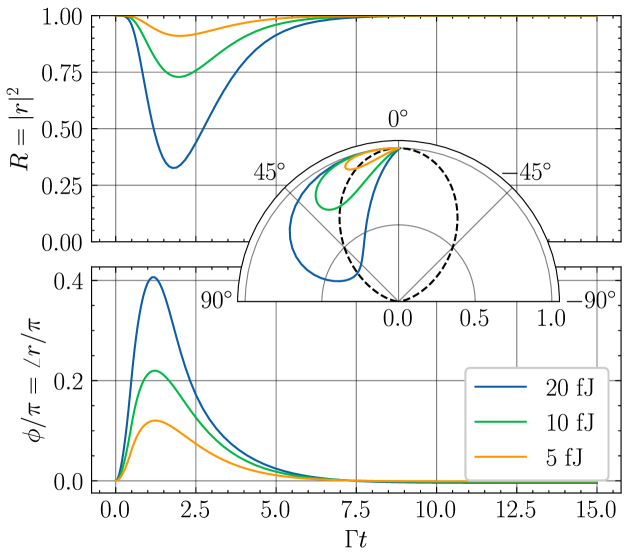
Fig. A1 plots the switching characteristics for the parameters in Table A1. Free-carrier dispersion dominates the response for the nanosecond-order timescales of interest followed by a slow (s-order), weak () thermal rebound. The three order-of-magnitude timescale difference effectively decouples the two modulation mechanisms. Note that the true reflection coefficient deviates from the Lorentzian response of a quasi-static cavity due to the fast (relative to the cavity decay rate ) carrier dynamics. These results indicate that a SLM with pixels operating with MHz could be realized with optical control power.
| Parameter | Value | Source |
|---|---|---|
| 3.48 | [107] | |
| 1.12 eV | [107] | |
| K-1 | [107] | |
| 1.64 J/cmK | [108] | |
| 0.26 cm2/s | [108] | |
| m3 | [109] (Linearized) | |
| 19 cm2/s | [55] | |
| 1 ns | [55] | |
| 1550 nm | Assumed | |
| 200,000 | Assumed | |
| 0.95 | [108] | |
| 220 nm | Measured | |
| Assumed | ||
| 0.5 ns | Assumed | |
| 0.6 | FDTD |
Appendix B Performance Comparisons
Table A2 compares the PhC-SLM demonstrated here to other actively-controlled, 2D SLMs (Fig. 1b). Wavelength-steered devices and switch arrays are omitted to restrict focus to the typical SLM architectures in Fig. 1. Notably, while beamsteering with PhC waveguides [47, 110, 111] and laser arrays [112] has recently been demonstrated, our device is the first (to our knowledge) to feature simultaneous emission from a 2D array of individually controllable PhC pixels.
| Class [Year] | Device | [] | [Hz] | ||
| EO [2022] | PhC-SLM | 64 | |||
| EO [2021] | polymer-coated grating [26] | — | |||
| EO [2019] | thin-film plasmonic resonator [25] | 20* | |||
| EO [2017] | Bilayer guided resonators [23] | 40* | |||
| EO [2011] | polymer-coated grating [33] | 18* | |||
| EO [2005] | MQW micropillar modulators [24] | 50 | |||
| Thermal [2018] | Asymmetric Fabry-Perot cavity [17] | 59 | |||
| Thermal [2013] | Waveguided phased array [16, 113] | 10* | |||
| MEMS [2019] | Grating phase shifters [20] | 85* | |||
| MEMS [2019] | Piston mirrors [21] | — | |||
| MEMS [2014] | High-contrast gratings [19] | 36* | |||
| MEMS [2001] | Piston mirrors [18] | 86 | |||
| LC [2020] | Plasmonic metasurface [14] | — | |||
| LC [2019] | “MacroSLM” [3] | 95 | |||
| LC [1994] | Binary ferroelectric LC [13] | 79 |
Appendix C Inverse Design Strategy
We implement the inverse design strategy in Fig. 3b using the open-source guided mode expansion (GME) package Legume [114]. GME approximates the cavity eigenmode using the incomplete basis set of waveguide modes in an “effective” unpatterned slab (in effect transforming the 3D eigenproblem to 2D) and perturbatively computes the loss due to coupling to the radiative continuum [77].
During each optimization step, we aggregate the losses of the fundamental slab mode over four Bloch boundary conditions at all wave vectors satisfying given the reciprocal lattice vectors . The objective function Eqn. 2 converges within tens of iterations, and the resulting design is then verified with using a grid in the Brillouin zone of the rectangular lattice of unit cells.
Exemplary GME-approximated far-field profiles for an cavity with two target quality factors are shown in Fig. A2a,c for comparison to those computed using near-to-far-field transformations of FDTD-simulated fields [115, 82]. These results confirm that the perturbatively-computed GME coupling coefficients can be used to accurately estimate a cavity’s far-field scattering profile.
The inverse design objective function (Eqn. 2) maximizes the directivity (for the light cone ) of the emission profile for any . The resulting aperture efficiency
| (15) |
compares to the maximum directivity of an area aperture at wavelength , and can therefore be interpreted as the fill factor of light scattered from an effective area . Fig. A3 compares for grating-coupled and inverse-designed cavities. For most inverse designs, regardless of . Since GME assumes periodic boundary conditions (indicative of the true array design), scattering from neighboring unit cells enables designs with . However, this “super-directive” performance is undesirable since the steerable field-of-view is narrowed to .
Appendix D Experimental Setups
Fig. A4 schematically illustrates the major components of our experimental setup. Here, we describe the design and function of each sub-assembly.
D.1 Near-Field Reflection Spectra
The wide-field, cross-polarized microscope in Fig. A4(a) allows us to simultaneously measure the reflection from every cavity within a camera’s field-of-view. A visible illumination path (not illustrated) is joined with collimated infrared light from a tunable laser with a dichroic mirror and focused onto the back-focal-plane (BFP) of an objective by lens L1. The angle-of-incidence and spot size of the infrared beam on the sample are therefore controlled by translating L1 and varying the collimated beam diameter, respectively. In our typical wide-field configuration, a 7.2 mm beam diameter focused to the center of a objective’s BFP yields a m waist-diameter, vertically-incident field that quasi-uniformly illuminates PhC cavity arrays.
By orienting the input polarization at a angle relative to the dominant cavity polarization axis (with a half-wave plate or by physically rotating the sample), light coupled into and reflected by the PhC cavity is polarization rotated and can be isolated from direct, specular reflections with a polarizing beamsplitter. A kHz-rate free-running, dual-band (visible and infrared) camera images this cross-polarized reflection signal through the tube lens L3. For each frame collected during a laser sweep, the wavelength is interpolated from the recorded camera and laser output triggers and each cavity’s reflection is integrated over a fraction of pixels within its imaged unit cell boundary. We use the resulting high-contrast reflection spectra (across all devices within the field-of-view) to characterize device performance and monitor the cavity trimming process.
The sample mount below the objective (OL) is temperature stabilized to within mK with a Peltier plate and feedback controller. For trimming experiments, the sample is placed in a high-pressure oxygen environment within a custom chamber offering in-situ optical access through a glass window.
D.2 Calibrated Far-Field Measurement
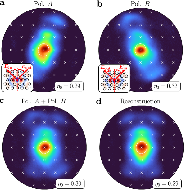
Inserting a lens (L2) in the collection path one focal length from the objective BFP allows us to measure the far-field profile of individual or multiple cavities using the same setup. We position an iris at the intermediate image plane — located with a removable lens (not shown) placed before L3 — to spatially filter the emission from desired devices. We also calibrate the BFP scale using a reflective reference grating with known pitch. Due to the cross-polarized configuration, only a single polarization is imaged for any cavity-input polarization angle difference . The complete cavity emission profile
| (16) |
can therefore be reconstructed by sequentially imaging both polarizations as in Figs. A5a-c for . For maximum accuracy, we used this technique for the experimental results in Fig. 4.
Alternatively, the specific choice allows to be reconstructed from a single measurement. Due to mirror symmetry about the cavity’s principal polarization axis , Fig. A5a-b show that for the reflection operator . This alternative reconstruction
| (17) |
is demonstrated experimentally in Fig. 4d, yielding excellent agreement with Fig. 4c. This technique simplifies high-throughput far-field measurements across cavity arrays (Fig. A10, for example).
D.3 Homodyne Measurement
The shot-noise-limited balanced homodyne detection setup in Fig. A4c enables complex reflection coefficient measurements with greater than 3 dB shot-noise clearance below GHz [108]. Signal light reflected from the cavity combines with a path-length-matched (to within mm based on time-delay measurements with a picosecond-class pulsed laser) local oscillator (LO), and both signals are coupled into a balanced detector using anti-reflection coated fibers. The in-phase () and quadrature () components of the cavity reflection were sequentially measured by locking to the first and second harmonics of the balanced output in the presence of a piezo-driven LO phase dither. The resonant, cross-polarized cavity reflection and phase shift are then reconstructed as
| (18) |
by normalizing to the measured peak voltage swing of the interference signal.
D.4 Parallel Cavity Trimming
A liquid crystal on silicon (LCOS) SLM (Fig. A4c) actively distributes a high-power, continuous-wave visible laser to target devices during the cavity trimming procedure. The input laser was tunably attenuated with a motorized half-wave plate (preceding a PBS) and subsequently expanded to overfill the LCOS aperture. The LCOS SLM was re-imaged onto the objective BFP (as confirmed by imaging with L2 in place) using two lenses (L4, L5) with focal lengths chosen to optimally match the imaged SLM and objective pupil dimensions. Phase retrieval-computed holograms then evenly distribute power to an array of focused spots on the sample (Appendix I) when the mechanical, flip mirror shutter is opened.
D.5 LED Imaging
The collection optics in Fig. A4d maximize the intensity of a LED array projected onto the PhC membrane within the constraints dictated by the constant radiance theorem of incoherent imaging. Assuming a Lambertian emission profile, geometric optics gives the collection efficiency for an objective lens (CL) with numerical aperture focused on the LED array. The projection efficiency through the projection objective (OL, with numerical aperture ) depends on the relative pupil sizes of both objectives and can be similarly approximated from geometric optics. The resulting intensity enhancement between the source and image (with magnification ) reaches a maximum when the CL-collimated light overfills the back aperture of OL. The resulting design criteria,
| (19) |
is achieved for our imaging setup with , , and . After CL, The overall magnification and rotation are fine-tuned with a variable beam expander and Dove prism, respectively.
Appendix E Optimum Gaussian Coupling
The far-field spatial overlap integral [116]
| (20) |
over the hemisphere at distance yields the power coupling between a cavity mode and fundamental Gaussian beam as a function of the Gaussian waist radius . We compute the cavity electric field profile by applying a near-to-far field transformation to the FDTD-simulated cavity mode in a plane just above and parallel to the PhC slab 444Flexcompute, Inc. Tidy3D. https://simulation.cloud [118]. The resulting far-field profile is finely discretized — relative to the diffraction-limited beamwidth for typical cavity unit cell dimensions and resonant wavelength — on a 1∘ grid in zenith and azimuth ( and , respectively). For the co-polarized Gaussian mode, we instead convert the magnetic field [88]
| (21) |
derived from paraxial diffraction theory (for the free space impedance ) to spherical coordinates at a far-field distance . Both modes are normalized to carry unit power .
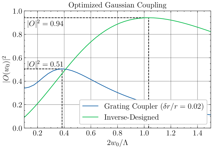
Fig. A6 compares the resulting power coupling as a function of normalized waist for grating-coupled and inverse-designed cavity designs with maximum dimension . In both cases, a backreflector is assumed for unidirectional emission into . Besides the increase in maximum coupling to 94%, the optimized waist diameter indicates that the inverse-designed cavity’s effective near-field scattering profile fully fills the design unit cell.
The power coupling to a single desired free-space mode also allows us to compute that mode’s amplitude reflection spectrum [88]
| (22) |
using temporal coupled mode theory assuming a normalized detuning from the cavity resonance and -directional emission (i.e. for unidirectional emission with a backreflector or for symmetric emission). Fig. 4 of the main text plots these optimized spectra. Whereas the grating-coupled cavity is undercoupled with an amplitude-dominant reflection spectrum, the inverse-designed cavity is phase-dominant as desired for high efficiency beamforming.
Appendix F Beamforming with a Coupled Amplitude-Phase Response
Phase retrieval algorithms (Appendix I) optimize unity-magnitude near-field reflection coefficients to generate a desired far-field intensity pattern, but fail for the coupled amplitude and phase reflection coefficients of Eqn. 22 [119, 120]. Here, we derive an alternative algorithm to compensate for this coupling.
Assuming a spatially uniform field incident on a -pitch array, the reflected far-field defined in Eqn. 3 is the product of the single-element far-field pattern and the array factor
| (23) |
i.e., the 2D discrete Fourier transform () of the reflection coefficients with respect to the cosine-space coordinates and . Since is determined by element design (Section II), far-field pattern synthesis is achieved by optimizing the array factor. Given Eqn. 23, we can represent constrained far-field synthesis with the nonlinear program
| (24) |
where is the matrix of reflection coefficients as a function of the detuning matrix , represents the complex modulus, is the Frobenius norm, and is the goal image. By normalizing the Fourier transforms, this program optimizes image appearance as opposed to absolute intensity, which varies in the presence of reflection loss.
We approximate the solution to the nonlinear program using the L-BFGS-B method — a low-memory quasi-Newton method with simple box constraints to limit detunings [121]. L-BFGS-B uses the gradient and a low-rank approximation of the objective function’s Hessian to approximate Newton’s method, yielding superlinear convergence.
To efficiently optimize Eqn. 24, we computed its analytic gradient
| (25) |
for
| (26) |
and
where and are the Hadamard/element-wise product and Frobenius inner product, respectively. Since Eqn. 25 contains only Fourier transforms and element-wise operations, it can be calculated in time.
We further accelerated L-BFGS-B by initializing with a modified phase retrieval algorithm that enforces near-field constraint [122]. The described algorithm was implemented in python using the PyTorch package for GPU acceleration. Using an RTX 2080, the generation of the far-field patterns for Fig. 3 took only a few seconds. The success of the algorithm is demonstrated by the lack of a conjugate image (even in the highly undercoupled case).
Appendix G Effect of Substrate Reflections
Isolated slab PhC cavities feature symmetric, bi-directional emission due to vertical reflection symmetry about the slab midplane. When placed above a reflective substrate, however, interference between the (reflected) downwards and upwards emission paths alters the cavity’s radiation pattern and [123]. The results are analogous to the modified spontaneous emission from a quantum emitter placed above a mirror [124].
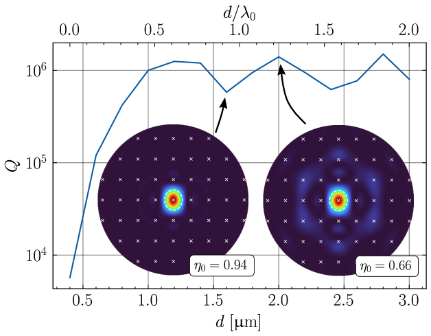
Fig. A7 plots the FDTD-simulated quality factor trends of an inverse-designed cavity as a function of the membrane-substrate gap spacing . Since the optical thickness of the PhC slab is approximately , constructive interference at () maximizes vertical emission and minimizes . Destructive interference at has the opposite effects. The resulting variation in explains the minor discrepancy between the simulated and measured in Fig. 4.
We mitigated the impact of these effects through optimized sample preparation. Compressive stress in our silicon-on-insulator (SOI) die buckles suspended cavity arrays, yielding variations in — and therefore cavity reflectivity — across the membrane. As an alternative to previously proposed stress-engineered support structures [125], we flattened the suspended arrays by mechanically bowing the die with a backside set pin in a custom sample mount (Fig. A8). Unfortunately, the resulting (uniform) gap spacing minimizes vertical coupling at the design wavelength . We therefore added a back-side silicon nitride anti-reflection coating (ARC) on the substrate and timed the release etch to form a front-side ARC with the remaining oxide (Fig. A9).
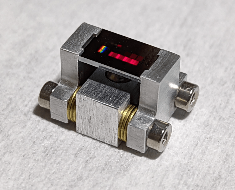
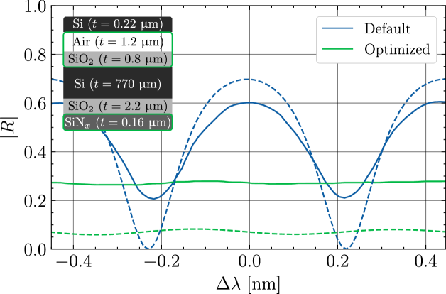
Appendix H Far-Field Uniformity
Fig. A10 demonstrates the far-field uniformity characteristic of inverse-designed and grating coupled cavity arrays. Averaged across the arrays, the former offers a improvement in zero-order diffraction and aperture efficiencies (, ).
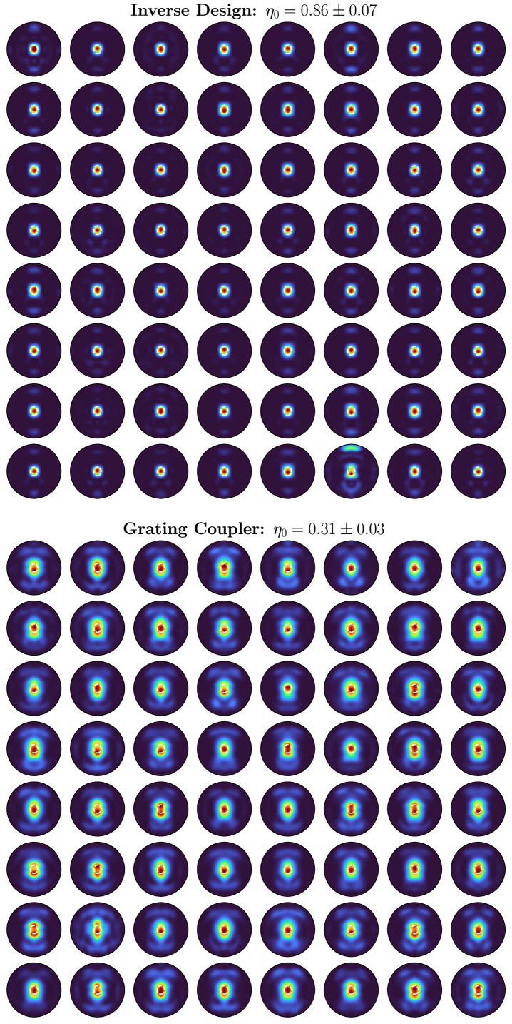
Appendix I The slm-suite Toolbox
We developed the open-source python package slm-suite to simplify the creation of high-uniformity, arbitrary-geometry optical focus arrays using various phase retrieval algorithms. The package features:
-
1.
Automated wavefront calibration routines that measure the Fourier-plane source amplitude and phase using a super-pixel interference technique to compensate for aberrations along the SLM imaging train [126]
- 2.
-
3.
Automated affine transformations between grating wave vectors applied to the SLM and image-space coordinates (i.e. camera pixels) by projecting and detecting a GS-computed spot array
-
4.
Camera-based feedback of measured spot amplitudes at known (calibrated) locations into phase retrieval algorithms to improve the uniformity of image-space spot arrays
-
5.
Automated evaluation metrics to monitor diffraction efficiency, spot amplitude and position tolerance, and spot quality.
-
6.
Simplified hardware interface and control.
After calibration, high-uniformity optical foci can be generated at arbitrary image plane locations specified by the user. For example, Fig. A11 shows a spot array with power uniformity and sub-micron placement accuracy formed on a cavity array during the trimming procedure of Section IV.
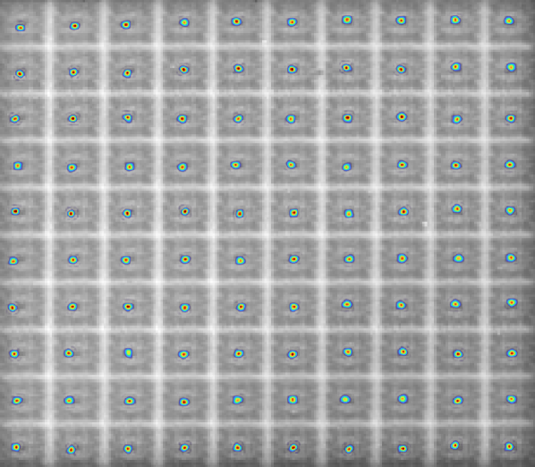
Appendix J Parallel Laser Oxidation
As illustrated by the wavelength trends as a function of incident laser power and exposure time in Fig. A12, we found that laser-assisted thermal oxidation could be accelerated in a high-pressure oxygen environment. We therefore mount samples in a custom pressure chamber with a partial oxygen pressure ranging from 5 to 10 atm.
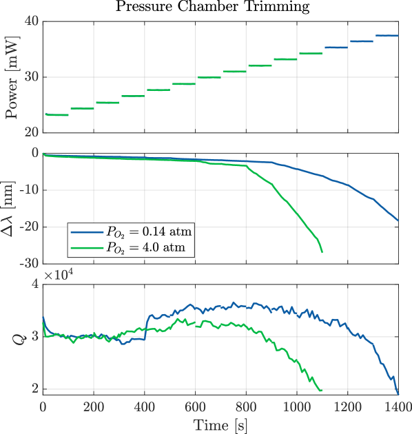
| Technique [Year] | Cavity Type | [pm] | In situ? | Parallel? | ||
|---|---|---|---|---|---|---|
| “Holographic” oxidation [2022] | Si PhC | 64 | 13 | Y | Y | |
| Germanium implantation [2021] | Si ring [130] | 58 | 32 | Y | N | |
| Laser-annealed cladding [2020] | Si ring [131] | 2 | 20* | Y | N | |
| Boron implantation [2019] | Si ring [132] | 4 | 15 | Y | N | |
| Electron-beam irradiation [2018] | Si PhC [133] | 4 | 400 | N | N | |
| Photo-electro-chemical etching [2017] | GaAs disk [134] | 5 | 200* | Y | N | |
| Annealed cladding [2016] | Si ring [135] | 5 | 90* | Y | N | |
| Ultraviolet irradiation [2014] | a-Si ring [136] | 4 | 45 | Y | N | |
| Post-fabrication etching [2013] | GaAs PhC [137] | 18 | 100* | N | Y | |
| Photochromatic thin-film [2011] | GaAs PhC [138] | 3 | 340 | Y | N | |
| Anodic oxidation [2006] | GaAs PhC [139] | 2 | 100* | N | N |
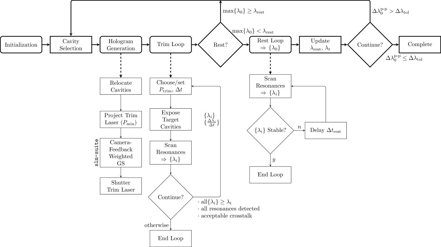
The main loop of the trimming process (Fig. 6) consists of device selection, hologram setup, parallel laser oxidation, and resting intervals. The algorithm monitors two resonant wavelengths: the instantaneous wavelength and the steady-state wavelength . Initially ; however, focusing high-power ( mW) visible light onto the cavity (as required to sufficiently heat the PhC membrane for thermal oxidation) causes a temporary blueshift due to the desorption of moisture attached to hydrophilic hydroxyl surface terminations. For any target rest wavelength , we therefore trim devices to an instantaneous wavelength that relaxes over timescales to as moisture re-adsorbs to the surface. In practice, the stability and estimation of the “overtune” limit the uniformity and scale of the trimming process, respectively.
After initializing the cavity locations, scanning the device resonances, and calibrating the SLM (Section I), a spot array targeting every cavity (Fig. A11, for example) is projected on the membrane for a short (few second) duration. Monitoring the resonances at fixed intervals s until stabilizes to the rest wavelength gives an initial estimate for the overtune parameter of each cavity. We also update the target wavelength and rest wavelengths before continuing the trimming procedure. To update , we periodically conduct this same “rest loop” when of each cavity is below an algorithmically chosen “checkpoint” wavelength .
As described in Section IV, a subset of cavities is then selected to maximize the total possible trimming distance to . The number of targeted cavities neighboring each untargeted cavity is also limited to reduce crosstalk. A spot array is then formed to evenly distribute the trimming laser to the selected devices. After confirming that the location accuracy and power uniformity of the array are within tolerance, we alternate exposure and readout intervals to grow thermal oxide with in situ monitoring. The laser power is progressively increased to reach a desired, wavelength-uniformity-dependent trimming rate. As evidenced by Fig. A12, the rate is relatively power-independent until reaching a threshold power. We detect and save these threshold powers for use when selecting the initial exposure power in each trimming loop.
The trimming sub-loop continues until the estimated of any targeted cavity crosses . New cavities are then selected, targeted, and trimmed until a rest period is triggered. When the peak-to-peak wavelength uniformity at the end of a rest period is below the user-defined tolerance , the process is terminated. Table A3 compares the demonstrated performance compared to other arrayed microcavity trimming techniques.