A high-sensitivity charge sensor for silicon qubits above one kelvin
Abstract
ABSTRACT: Recent studies of silicon spin qubits at temperatures above 1 K are encouraging demonstrations that the cooling requirements for solid-state quantum computing can be considerably relaxed. However, qubit readout mechanisms that rely on charge sensing with a single-island single-electron transistor (SISET) quickly lose sensitivity due to thermal broadening of the electron distribution in the reservoirs. Here we exploit the tunneling between two quantised states in a double-island SET (DISET) to demonstrate a charge sensor with an improvement in signal-to-noise by an order of magnitude compared to a standard SISET, and a single-shot charge readout fidelity above 99 % up to 8 K at a bandwidth kHz. These improvements are consistent with our theoretical modelling of the temperature-dependent current transport for both types of SETs. With minor additional hardware overheads, these sensors can be integrated into existing qubit architectures for high fidelity charge readout at few-kelvin temperatures.
KEYWORDS: Quantum computing, silicon, quantum dot, single-electron transistor, charge sensing, temperature
I Introduction
Quantum computers may be realised by exploiting electron or nuclear spins as quantum bits (qubits) in silicon.Loss and DiVincenzo (1998); Kane (1998); Morton et al. (2011); Zwanenburg et al. (2013); Veldhorst et al. (2017); Vandersypen et al. (2017) The spins of electrons in lithographically defined quantum dots have proven to be a prime candidate for a scalable quantum computer architecture by virtue of their long coherence time, high fidelity and compatibility with modern metal-oxide-semiconductor (MOS) technology.Ladd and Carroll (2018); Gonzalez-Zalba et al. (2020) Most early demonstrations of this technology were performed in dilution refrigerators at temperatures around 100 mK, where the cooling power of the cryostats is strongly limited and orders of magnitude smaller than at few-kelvin and beyond.Jazaeri et al. (2019); Hornibrook et al. (2015); Degenhardt et al. (2017)
Going to higher temperatures, the qubits may be operated in isolated mode, decoupled from the thermally broadened electron reservoir Bayer et al. (2019); Yang et al. (2020) and read out using Pauli spin blockade. Jones et al. (2018); Fogarty et al. (2018); Zhao et al. (2019); Yang et al. (2020); Seedhouse et al. (2021) Demonstrations of one- and two-qubit operation above 1 K were recently performed with these techniques Yang et al. (2020); Petit et al. (2020). Both works report reduced readout visibility at high temperatures, ascribed to the decreased sensitivity of the employed SISETs. This is because the broadened electron energy distributions in the leads allow for current even when the dot chemical potential is not aligned between the reservoir chemical potentials. The reduction in signal also limits the readout bandwidth, which will be problematic for detecting and correcting qubit errors – a problem that is amplified by the degraded spin lifetime and coherence time with increasing temperature. Petit et al. (2018); Yang et al. (2020)
In this letter we develop and test a temperature-resistant charge sensor based on a DISET, and compare it directly to a SISET obtained by disabling one of the tunneling barriers in the same device. We extract the amplitude and full-width-half-maximum (FWHM) of the Coulomb peaks of the DISET and the SISET from 1.7 K to 12 K and find good agreement with our theoretical model. Furthermore, we sense charge transitions in a nearby quantum dot both in low-frequency AC lock-inElzerman et al. (2004); Yang et al. (2012) and single-shotGotz et al. (2008) measurements. We quantify the sensing performance for both schemes by calculating the signal-to-noise ratios (SNR) and error probabilities for single-shot sensing. The DISET offers significantly higher SNR and fault-tolerant charge readoutFowler et al. (2009, 2012); Knill (2005) up to 8 K at the full nominal bandwidth of 200 kHz of our setup. Under the same conditions, the signal of the SISET is already below the noise amplitude. Taking into account the impact of temperature on spins Yang et al. (2020) and measurement bandwidth, we determine that fault-tolerant readout fidelities ( %) can only be achieved with a SISET operated below 1.6 K while the DISET can operate above 4.2 K, conveniently achievable with a liquid 4He cryostat.
II Experimental Methods
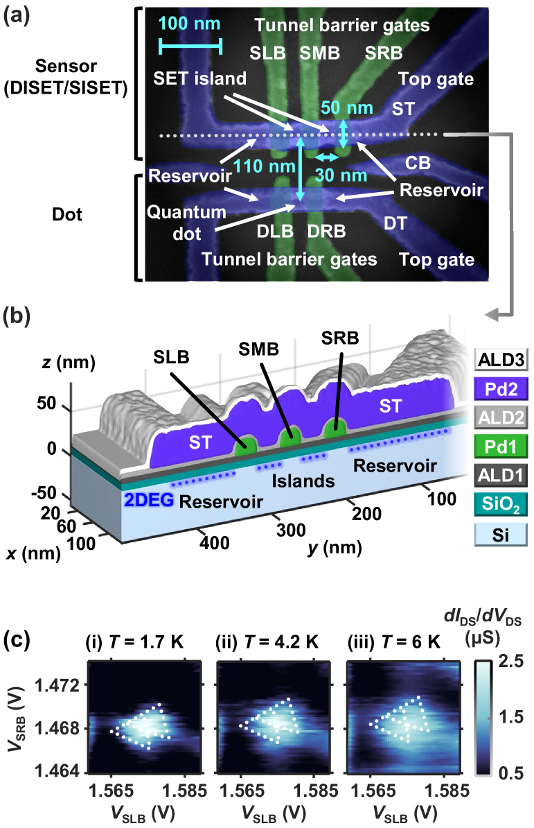
Figure 1(a) is a scanning electron micrograph (SEM) of a device nominally identical to the one measured in this work. It consists of a natSi substrate, thermally grown SiO2, and a two-layer Pd gate stack with atomic-layer-deposited AlxOy (ALD) in between (details in Supporting Information A). A top gate accumulates a two-dimensional electron gas (2DEG) under the Si/SiO2 interface, forming the electron reservoirs [see Figure 1(b)]. The tunnel barrier gates then electrostatically define the sensor quantum dotLim et al. (2009a, b); Angus et al. (2007) as Figures 1(a)-(b) indicate. If the sensor SRB is biased to form a potential barrier, it constricts the transport to single-electron tunneling and the sensor is configured as a DISET. However, if SRB is biased above threshold, the reservoir is extended and the sensor becomes a SISET using only the left island from the DISET. The dot in the lower structure in Figure 1(a) acts as our device-under-test for the charge sensing measurements.
III Transport
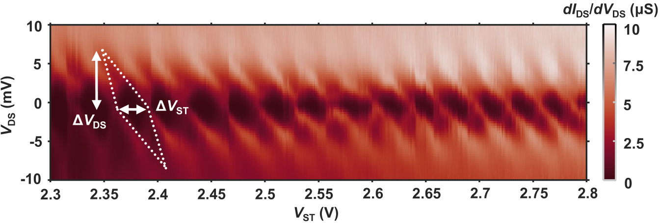
Transport characteristics are measured using an AC lock-in amplifier with a source-drain excitation of 0.2 mV at 191 Hz. Figure 1(c) shows the differential conductance of the DISET as a function of the voltage on SLB and SRB. We apply a DC source-drain bias mV, which creates a triangular region in voltage space with enhanced current (called bias triangles).Lim et al. (2009a); van der Wiel et al. (2002) These regions occur near the triple points where states with different charge configurations are degenerate. The sensor top gate ST is biased at 2.92 V, much higher than the turn-on voltage of 1.66 V in this device, to enhance current. The middle barrier gate between the two sensor islands SMB is biased at 1.26 V, in which case cotunneling is mostly suppressed. Figure 1(c) shows a typical triangle pair in a well-tuned regime, of which a larger scan is shown in Supporting Information B. The triangle pair broadens progressively as we increase the device temperature from 1.7 K to 6 K. The sides of the triangles correspond to the alignment of the Fermi level in the reservoirs to the energy level in the neighbouring island, whereas the base corresponds to the alignment of the energy levels of the two islands.van der Wiel et al. (2002) Comparing Figure 1(c)(i)-(iii), we see more broadening on the triangle sides when the temperature increases, as expected. Additionally, cotunneling and background current appear more prominent with increasing temperature while the peak current reduces.
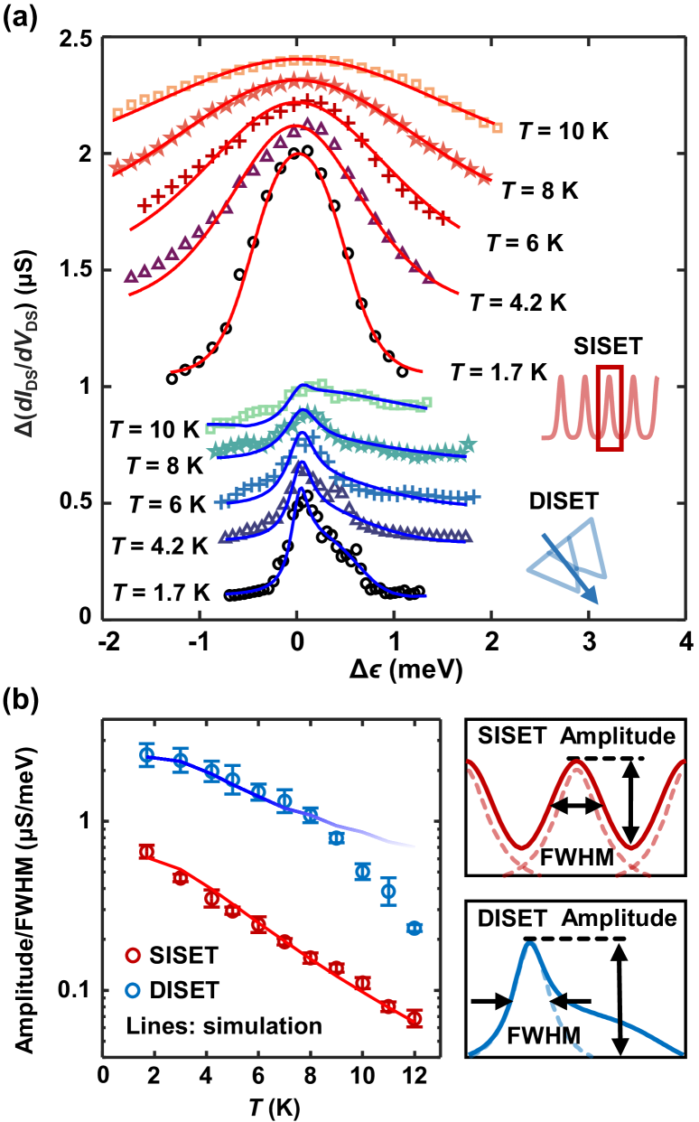
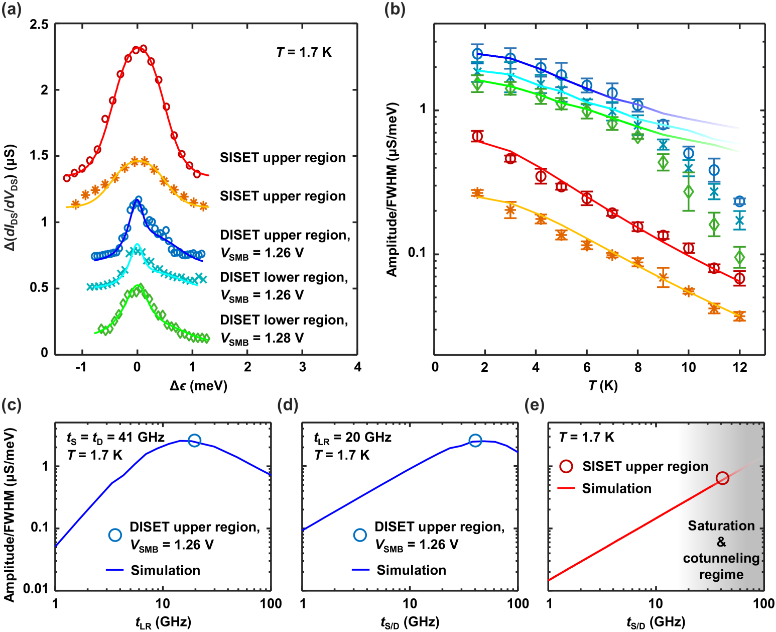
In order to study the DISET sensitivity to electrostatic potential changes in the environment, we measure the differential conductance in response to detuning , which is converted from gate voltage using relevant lever armsLim et al. (2009a); Fujisawa et al. (1998) (Supporting Information B). The steepness of the peaks can be estimated using the amplitude divided by the full-width-half-maximum (FWHM), which quantifies the change in differential conductance per unit potential shift. Figure 2 shows a comparison between the SISET and the DISET, both biased for maximal slope to the best of our ability. We acquire the SISET peaks by sweeping ST and the DISET peaks by sweeping SLB and SRB in opposite directions, which is equivalent to a line cut through a triangle [see Figure 2(a)-insets]. We see from Figure 2(a) that throughout the temperature sweep, the DISET peak is evidently steeper at compared to , and the broadening appears to be more evident as the temperature rises. We extract the FWHM from this dominant peak at and compare the extracted slope to that of the SISET in Figure 2(b). At the same temperature, the DISET offers markedly larger slope than the SISET and this advantage increases until around 8 K. At that point, the DISET degrades faster than the SISET, which we associate to the limit where the thermal broadening becomes larger than the Coulomb blockade quantisation window in the islands.
We develop a theoretical model for the transport through the quantised DISET levels to understand the experimental transport characteristics. The details of the model and analytical treatment of the equations are presented in Supporting Information C. The resulting expression for the total DISET current is
| (1) |
where is the unit charge,
| (2) |
and is the sum of all numerators. The transition rates are defined as follows:
| (3) |
| (4) |
| (5) | ||||
| (6) |
and describe the Fermi-Dirac distribution in the source and drain reservoirs, whose Fermi levels are and as set by the source-drain bias. The temperature is denoted by , and and denote the energy levels in the left and right island respectively. The relevant rates are the reservoir-island tunnel rate , , inter-island tunnel rate and inter-island relaxation rate .
Using this model, we tune the DISET and the SISET to their near-optimal sensing regime (details in Supporting Information D). In Figure 2, we bias the DISET at V, V and V. To operate the SISET, we apply V and V, while setting V to extend the reservoir into the DISET right island location. The peaks are further enhanced when a DC bias mV is applied. We choose a Coulomb peak near V to compare the SISET sensitivity to that of the DISET.
The measured DISET peaks in Figure 2(a) are fitted to Equation 1 without major disagreement (error %), confirming the quantitative validity of the model. At low temperature, the error is dominated by current fluctuations due to charge noise. Starting from 6 K, we see a different type of broadening around the resonant peak, which signifies additional physical processes. The steeper slope at stems from inter-island resonant tunneling.Stoof and Nazarov (1996); Fujisawa et al. (1998) At , inter-island relaxation current due to acoustic phonon emission also contributes, forming a shoulder that partially masks the resonant peak.Fujisawa et al. (1998); Wang et al. (2013) This relaxation current has negligible effects on the quality of the DISET current peaks. We also notice that the width of the shoulder deviates from in some of the peaks, possibly because the sweep direction is not exactly perpendicular to the triangle base, or there is variation in and especially at high temperatures. In Figure 2(b), after necessary conversions and assuming constant rates, we fit the data to Equation 1 with error % up to 8 K. We extract GHz and the overall contribution from and GHz. Since has no influence on the DISET FWHM, we extract GHz at 1.7 K from the 1D peak in Figure 2. We notice a deviation from 8 K onward possibly attributable to orbital excitationYang et al. (2012), which is not considered in our model.
We also fit the SISET data to the expression for single-island transport current:Ihn (2015)
| (7) |
We see no apparent deviation between the measured and simulated data. The fit errors in Figure 2(a) and (b) are %, mainly arising from potential fluctuations at lower temperatures (which are negligible at higher temperatures). The average contribution from and is GHz, close to that in the DISET.
Equations 1 and 7 suggest a predominantly exponential decay in the slope of the DISET and the SISET Coulomb peaks over temperature. The decay is notably slower in the DISET case. These characteristics are verified by the experimental data up to 8 K. Moreover, the offset between the two curves is related to the tunnel rates and source-drain bias in both SETs, which depend strongly on device tuning.
IV Charge Sensing
We now employ the DISET and the SISET as charge sensors. To capture charge transitions in the quantum dot, we apply an AC excitation to DT with an amplitude of 2 mV and a frequency of 127 Hz, then demodulate the sensor current at this frequency to obtain the signal correlated to variation.Yang et al. (2012); Elzerman et al. (2004) We operate the sensor near the optimal regime identified in Section III and tune it to the edge of a Coulomb peak where the highest slope is found. We apply dynamical compensationYang et al. (2011) on ST, SLB and SRB when sensing with the DISET and on ST when sensing with the SISET. We further increase to 1.5 mV in the DISET to enlarge the triangles without causing apparent variation to the sensitivity. We sweep DT between 1.75 V and 2 V while also varying DLB, DRB by V around 1.09 V and 1.2 V.
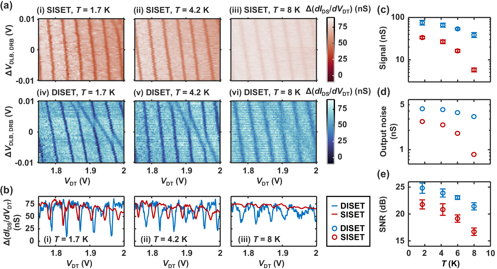
Figure 3(a) shows the resulting signal for the SISET (top row) and the DISET (bottom row) from 1.7 K to 8 K. Both SET configurations are stable during the sweeps and detect a number of transitions. In addition, we also observe the transition from a strongly-coupled parasitic dot, as indicated by the line with dissimilar slope and smaller amplitude in Figure 3(a) (i) and (iv) - (vi).Yang et al. (2011) Figure 3(b) shows the 1D traces along at around V and V. From the traces, we quantify the charge sensing performance by calculating the signal, noise and SNR, as shown in Figure 3(c) - (e). We calculate the signal by averaging over the dips in the traces and the noise by taking the standard deviation of the flat region in between transitions. The SNR is then given by . We see that the DISET signal is about twice that of the SISET at 1.7 K and becomes almost an order of magnitude larger at 8 K. The noise exhibits a similar temperature dependence, since the SET islands are sensitive to any electrostatic noise in the environment. It can also be inferred that the degradation in the SET sensitivity outpaces the linear increase in charge noise over temperature.Petit et al. (2018) Overall, since the DISET is more sensitive to both the charge transition and charge noise, the SNR is limited to a few dB higher than in the SISET case.
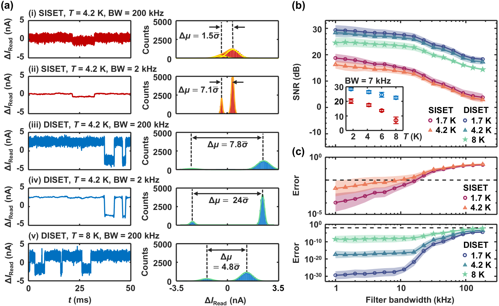
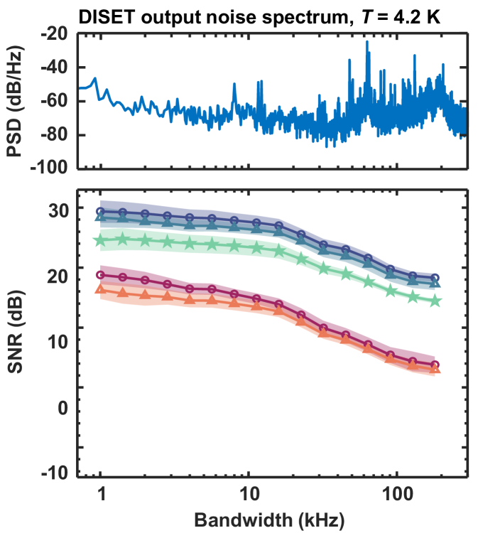
Lastly, we assess the charge sensitivity of SISET and DISET by performing single-shot charge readout of the nearby quantum dot.Gotz et al. (2008) We tune the sensors to their sensitive points and the dot to a charge transition point using lock-in sensing.Eenink et al. (2019) We then switch off the lock-in excitation and measure time traces at a nominal bandwidth of 200 kHz and a sample rate kHz. To study the effect of lower measurement bandwidths, we numerically filter the raw traces with Butterworth low-pass filters of varying cutoff frequencies. To approximate the band-limiting effect in the experiment, the filters are designed to have , where is the sample rate, and are the upper edge of the pass band and the lower edge of the stop band. Figures 4(a)(i) - (iv) show the vertically aligned current traces and the corresponding histograms for the SISET and the DISET at 4.2 K at a bandwidth of 200 kHz and 2 kHz. Each histogram pair is fitted to a double Gaussian with separation and average standard deviation . In Figure 4(a)(v), we demonstrate the DISET working at 8 K and a full effective bandwidth of 200 kHz, where the SISET signal is completely indistinguishable from the noise. We see that a higher temperature produces a smaller signal (), while a higher bandwidth yields larger noise (). Figure 4(b) shows the SNR calculated using , as a function of bandwidth at 1.7 K, 4.2 K for both SETs, and additionally at 8 K for the DISET. We average over 30 traces at each temperature. The upper bound for the bandwidth in our experiment is 200 kHz, which corresponds to the nominal amplifier bandwidth and a digitally-unfiltered signal, and the lower bound is 1 kHz, below which significant damping of the signal occurs. At the same temperature, the DISET SNR is at least 10 dB higher than that of the SISET and the difference slightly increases towards higher frequencies. The SNRs of both SETs experience a rapid decrease after kHz, which can be associated with the noise spectrum shown in Supporting Information E.
We also perform a temperature sweep at a bandwidth of 7 kHz and plot the temperature dependence in the inset of Figure 4(b). Here we see a decay consistent to the one observed earlier. However, in comparison to the lock-in measurements in Figure 3(e), we note that at 1.7 K both SETs begin with a higher SNR which then follows a faster decay. Moreover, a more significant improvement in SNR is observed for the full temperature range. This is because in the lock-in measurement, low-frequency charge noise dominates, whereas in the single-shot measurement, higher-frequency noise from the measurement setup dominates. The data implies that the DISET holds an even larger advantage over the SISET in the high measurement bandwidth regime.
We estimate the readout error from the double Gaussian fits to the histograms in Figure 4(a).Yang et al. (2020); Medford et al. (2013) Plotted in Figure 4(c), the error rate shows an agreement with both the temperature and bandwidth dependence of the SNR. We consider the fault-tolerant threshold, which specifies the maximum allowable error in quantum computation given a certain error correction protocol. If we set this threshold to be 1 % (or readout fidelity %), the SISET must measure at a bandwidth below 20 kHz at 1.7 K, or below 2 kHz at 4.2 K based on the estimation. On the other hand, this readout fidelity is achieved by the DISET at all measurement conditions in our experiment. Assuming that its performance is maintained at even higher bandwidths, we infer that the DISET would enable fault-tolerance for qubit temperatures exceeding 4.2K.Yang et al. (2020); Petit et al. (2020)
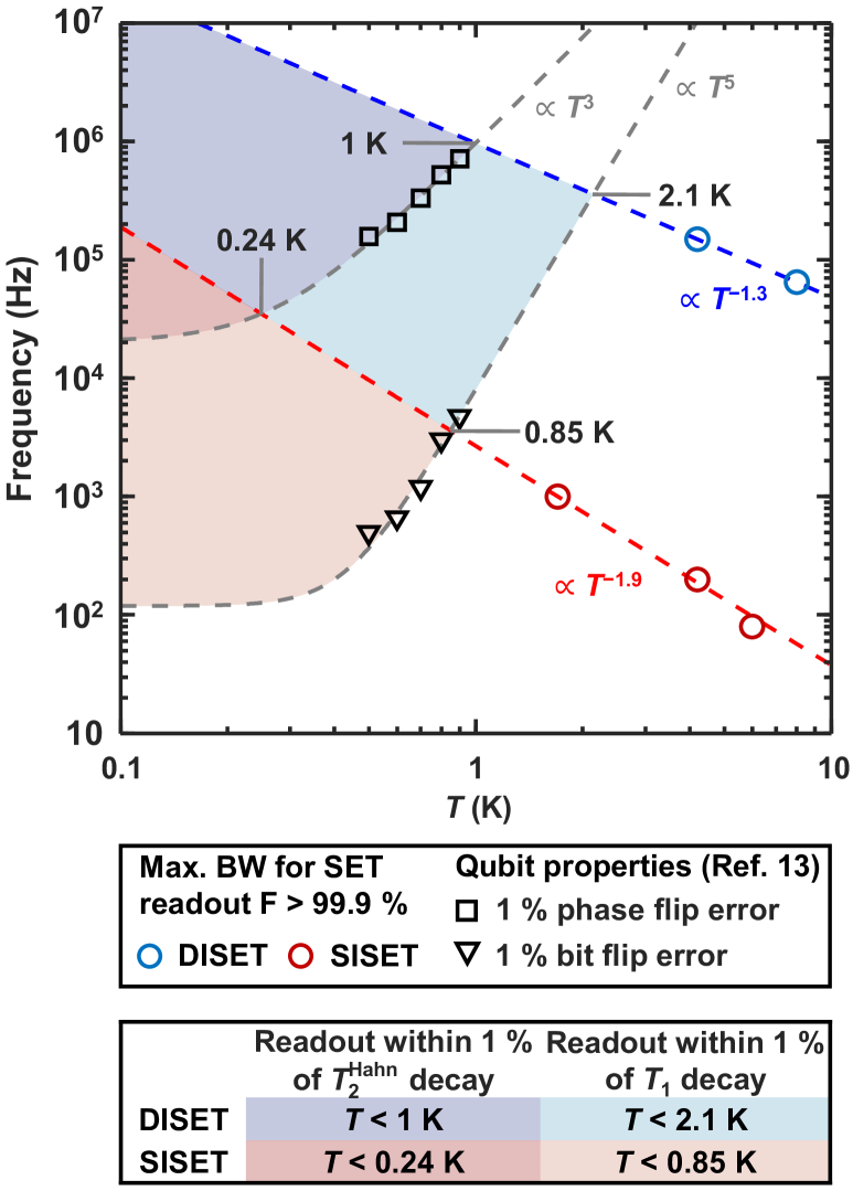
In Figure 5, we numerically explore the limits in operation temperature. Now we set a readout error threshold of 0.1 % and extract the maximum allowable measurement bandwidth from the experiments in Figure 4(c). This threshold value gives the maximum bandwidth for the DISET at 4.2 K, 8 K (blue circles) and that for the SISET at 1.7 K, 4.2 K and 6 K (red circles). The other curves do not cross this threshold level. We extrapolate from the above data points using polynomial fitting, which shows a dependence for the DISET (blue line) and a dependence for the SISET (red line). We also plot the inverse of the time for reaching 99 % of and decay in a silicon qubit above 1 K, calculated from the data in Reference (13). The crossing between the curve for 99 % of and the maximum bandwidth for the sensor provides a crude indication of the maximum temperature for readout, since provides the ultimate limit in spin readout. Above this temperature, the faster decay of spins requires a higher readout bandwidth from the sensor, which will subsequently compromise on the readout fidelity due to the loss of sensitivity. In our device, such limit for the SISET and the DISET are 0.85 K and 2.1 K, respectively, which suggests that the DISET is competent in performing fault-tolerant readout above the base temperature in pumped 4He cryostats.
V Conclusion and Outlook
In conclusion, we have fabricated and measured a sensor that can be configured as either a SISET or a DISET to sense charge transitions in a nearby quantum dot at elevated temperatures. We observe the temperature dependence of Coulomb peaks when the SETs are well-tuned. We develop a theory for the DISET which accounts for both the inter-island resonant tunneling and relaxation, finding good agreement between the theory and experiment up to 8 K. The DISET peaks offer appreciably larger slope at 1.7 K and broaden at a % slower rate when temperature is raised, as compared to the SISET in our operating regime. We apply both SETs in lock-in and single-shot charge sensing and demonstrate a considerably better signal with the DISET. This advantage becomes more pronounced with increasing temperature or higher measurement bandwidth. The DISET maintains a fidelity % even at 8 K, more than 100 times the temperature of the silicon qubits in dilution refrigeratorsHuang et al. (2019); Veldhorst et al. (2015, 2014) and more than four times the temperature in recent hot qubit experiments.Yang et al. (2020); Petit et al. (2020)
Our single-shot measurement data suggest that a DISET, similar to the one we measured, can operate at above 4.2 K, the temperature of liquid 4He, with a charge readout fidelity exceeding 99 %. In comparison, our SISET operation temperature is limited to 1.6 K in order to achieve the same fidelity. This finding will potentially benefit qubit readout above 1 K in the near future. Combined with the temperature-robustness of isolated mode operation,Yang et al. (2020); Petit et al. (2020) we expect to clear another challenge towards a silicon quantum computer that operates at few-kelvin, which is essential for the scalability of quantum processors.
DATA AVAILABILITY
The data supporting the findings in this study are available from the corresponding authors upon reasonable request.
ACKNOWLEDGEMENTS
We thank Ensar Vahapoglu, Santiago Serrano and Tuomo Tanttu for assistance in the cryogenic measurement setup. We acknowledge support from the Australian Research Council (FL190100167 and CE170100012), the US Army Research Office (W911NF-17-1-0198) and the NSW Node of the Australian National Fabrication Facility. The views and conclusions contained in this document are those of the authors and should not be interpreted as representing the official policies, either expressed or implied, of the Army Research Office or the U.S. Government. The U.S. Government is authorized to reproduce and distribute reprints for Government purposes notwithstanding any copyright notation herein.
CONTRIBUTIONS
JYH performed all measurements and all calculations. WHL and FH fabricated the devices. WHL, CHY and AL supervised all measurements. WHL, RCCL, CHY, AS, AL and ASD participated in data interpretation and experiment planning. CHY, CE and AS supervised the numerical modelling. AS supervised the model development and analytical derivations. AS, AL and ASD designed the project and analysed the results. JYH, AS and AL wrote the manuscript with contributions from all authors.
SUPPORTING INFORMATION
The Supporting Information is available free of charge on the ACS Publications website at
https://doi.org/10.1021/acs.nanolett.1c01003.
Device and measurement setup details, lever arms and tunability, DISET transport theory, transport characteristics and SET tuning, output noise spectrum.
Supporting Information: A high-sensitivity charge sensor for silicon qubits above one kelvin
A Device and measurement setup details
The device is fabricated on natSi substrate with diffused source (S) and drain (D), defined by photolithography. A two-layer Pd gate stack is patterned by electron beam lithography (EBL) and deposited using physical vapour deposition (PVD), with atomic layer deposited (ALD) AlxOy acting as insulator in between and around.Zhao et al. (2019); Brauns et al. (2018) Tunnel barrier gates for the sensor (SLB, SMB, SRB) and dot (DLB, DRB) are patterned together in the bottom layer (green); sensor and dot top gate (ST, DT) and confinement barrier gate (CB) are patterned in the top layer (blue). In all imaged devices, the CB gate is not fully formed, most likely due to the collapse of the polymethyl methacrylate (PMMA) resist that defines the geometry of the lithographically defined gates. We measure the device in an ICE Oxford variable temperature insert (VTI) that can operate from 1.7 K to room temperature. DC biases on the gate electrodes are supplied by QDevil QDAC voltage generators. The AC lock-in measurements for transport and charge sensing are conducted using Stanford Research Systems SR830 lock-in amplifier. A FEMTO DLPCA-200 transimpedance amplifier is also used for amplification and filtering. In the single-shot measurements, time traces are recorded via a Pico Technology PicoScope 4824 digital oscilloscope, after amplification by the FEMTO DLPCA-200 amplifier and a Stanford Research Systems SR560 voltage amplifier.
B Lever Arms and Tunability
Lever arms are required for converting voltage detuning into energy detuning , as well as to understand where the islands form in comparison to the gates. For the DISET, we first estimate the lever arm of SLB to the left island and that of SRB to the right island according to the formula .Lim et al. (2009a); Lai et al. (2011); van der Wiel et al. (2002) We also consider the cross-coupling from SLB to the right island and from SRB to the left island, which give rise to and . The voltage variations , , and are labelled in Figure S1(a). Under the biasing condition in Figure S1, we have , , and . It appears that SRB has more control over both islands than SLB. When we increase from 1.26 V to 1.28 V, and decrease to 0.13 and 0.30, suggesting that the islands are moving closer towards SMB.Eenink et al. (2019) However, and also decrease to 0.06 and 0.09, implying that the right island is less coupled to SLB and likewise for the left island. This is most likely because such cross-coupling is limited by the screening from the adjacent island, which becomes stronger as the islands come closer. Further increasing , we see the splitting of the triangles and the emergence of cotunneling lines [Figure S1(b)(i)-(ii)], which signifies a transition from the weak-coupling regime to the strong-coupling regime. The double-island system is thus highly tunable.
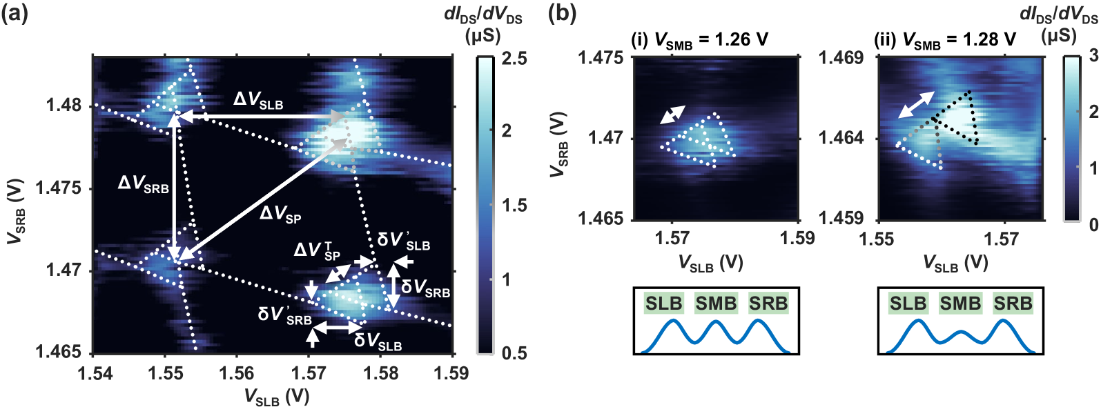
We also study an upper triangle pair at V but with similar and . In this case, , , and . The SRB lever arm here is smaller than that with lower , which is understood to be caused by an increased occupancy. While the gate capacitance remains approximately unchanged, the total island capacitance increases, therefore a smaller lever arm results according to .van der Wiel et al. (2002)
We notice that in all cases, is almost twice as large as , indicating a much stronger coupling between SRB and the right island compared to that between SLB and the left island. For this reason, we see notably more Coulomb peaks when sweeping along the direction in the window between pinch-off and saturation. We thus operate primarily around different to observe the effect of reservoir-island tunnel rates.
C DISET Transport Theory
In this section, we derive the expression for the total DISET current, as shown in Equation 1 in the main text. We describe the DISET with the Hubbard ModelHubbard and Flowers (1963); Das Sarma et al. (2011); Wang et al. (2011) and follow a Master EquationLindblad (1976); Gorini et al. (1976) approach. Previous studies have calculated either the inter-island/dot resonant tunneling currentStoof and Nazarov (1996); van der Wiel et al. (2002); Fujisawa et al. (1998); Gurvitz and Prager (1996); Gurvitz et al. (1996) or the relaxation currentTouati et al. (2014); Chao Zhang et al. (2010); Boubaker et al. (2009); Brenner (2004) alone. Here we develop a complete model that accounts for both the elastic transport and the inelastic transport.
We consider the DISET as an open quantum system, in which electrons occupying discrete energy states in the islands also interact with the environment through the reservoirs. This allows us to study the electron occupation by solving the Lindblad master equationLindblad (1976); Gorini et al. (1976) for density matrix . We then calculate the steady state current from the electron flow rate, which can be derived from .
The Lindblad equation we use takes the form
| (S8) |
where
| (S9) |
The Hamiltonian is Hermitian and are jump operators. The first term in Equation S8 originates from the von Neumann equation and describes the elastic processes, such as the inter-island resonant tunneling in our case. The second term, known as the Lindbladian dissipator, describes inelastic or dissipative processes, such as the reservoir-island transport or the inter-island relaxation.
We describe our coupled double-island system using the Hubbard model HamiltonianHubbard and Flowers (1963); Das Sarma et al. (2011); Wang et al. (2011)
| (S10) |
which is written in the basis , describing the state of no additional electrons, one additional electron in the left island and one additional electron in the right island (with respect to a certain number of electrons in either dots, depending on the particular bias triangle that we are operating on). The diagonal elements represent the total energy required for each state, while the off-diagonal elements represent the elastic tunnel coupling. For simplicity we set our zero energy to be aligned with the dot in the state. The energies and comprise potential offsets, background charge, local charge repulsion and inter-island charge repulsion. Elastic coherent tunnel coupling is considered only between and – all transitions involving the reservoirs are considered to be elastic but any coherence quickly decays. This means that the zero row and column in the Hamiltonian describe a state that only couples to the other states mediated by the Lindbladian dissipator.
The Lindbladian dissipator reads
| (S11) |
in which
| (S12) |
The operators describe the inelastic transitions between states at rates , which are determined as follows:
| (S13) |
| (S14) |
| (S15) | ||||
| (S16) |
Here , and are the tunnel rates between the source and the left island, between the left and the right island and between the right island and the drain. The inter-island relaxation rate is , and is the Fermi-Dirac distribution in the reservoir, expressed as
| (S17) |
where is the electron temperature and , are the chemical potentials at the source and drain.
| (S18) |
| (S19) |
Likewise, the von Neumann term (Equation S10) can be reshaped as
| (S20) |
Substitution of Equations S18 and S20 into Equation S8 with the steady state condition will result in a set of nine linear equations. We reduce the system of equations to those containing populations:
| (S21) |
The solution to the populations in Equation S21 is given by
| (S22) |
where
| (S23) |
and is the sum of all numerators. Notice that the populations and currents only depend on the inter-dot elastic tunneling through , such that it completely determines how the tunnel barrier control will impact the performance of the DISET. Comparing this term to the derivations in Reference Brenner, 2004, our model gives special attention to this elastic tunneling, which is an important ingredient for the added robustness of our device against elevated temperatures.
The steady state current through the system can be calculated using the current operator :Stoof and Nazarov (1996)
| (S24) |
where is a sum over , the probability current between state and : Hovhannisyan and Imparato (2019)
| (S25) |
Here and represent the basis states and . This current originates from the equilibrium electronic state transitions and the expression is a statistical equivalent of the formula . We also note that for our DISET with series-connected islands and reservoirs, the current continuity condition makes necessary that the transport current between any two states be equal in our three-state model. The above considerations lead us to substitute Equation S25 into Equation S24, with trivially chosen as . We arrive at
| (S26) |
Using the result for and from Equation S22, we end up with
| (S27) |
where and have been defined in Equation S23 and Equations S13-S15.
This is the minimum model that can describe a DISET. Hence Equation S27 accounts for a single bias triangle. Nevertheless, this model combines resonantStoof and Nazarov (1996) and relaxation currentBrenner (2004) as separately presented in previous literature. If we set and , we recover the expression for a purely resonant process,
| (S28) |
as derived in Reference (32). This is a Lorentzian function and is characteristic of a resonant peak in an SET without any dissipation. On the other hand, if we set , vanishes which leads to an expression of purely dissipative current:
| (S29) |
as found in Reference (52). Finally, we note that in Equations S27 and S28, and are indistinguishable, therefore we can only extract their mean contribution when fitting such formulas to experimental data.
D Transport characteristics and SET Tuning
In this section, we elaborate on how the barrier gate voltages influence the transport current in the DISET and the SISET, and explain the dependence using SET transport theory (Equation 1 and Equation 7 in the main text). This provides useful information for tuning the sensor, especially when it operates as a DISET. In all simulations, we assume a DC source-drain bias of mV for the DISET and mV for the SISET. The curve fitting are performed in terms of differential conductance. Figure S3(a) shows a typical peak at each biasing condition at 1.7 K for both SETs, and Figure S3(b) shows the temperature dependence of amplitude/FWHM averaged over five peaks at each condition. We estimate the tunnel rates from the fitting of the temperature dependence curve in Figure S3(b), and estimate the inter-island relaxation rate at a certain temperature from the fitting of the corresponding 1D peaks.
With fixed at 2.92 V, the tunnel rates , and are predominantly determined by , and . We first study a bias triangle pair in a lower region of the DISET occupancy map, where and are around 1.57 V and 1.47 V, respectively. We increase from 1.26 V to 1.28 V and observe the corresponding change in a Coulomb peak [Figure S3(a), cyan and green]. By fitting the curves to Equation 1 in the main text, we find that increases from GHz to GHz, while the mean of and also increases slightly from GHz to GHz. This indicates a transition from the regime where inter-island tunneling limits the current to a regime where reservoir-island tunneling is the bottleneck for current. This attests to the control that SMB offers over , in good agreement with the result in Figure S1. As can be seen in Figure S3(a), a higher and resulting higher increase both the amplitude and FWHM of the peak.
Additionally, we find that for V and 1.28 V, at 1.7 K and in the lower occupancy regime, the inter-island relaxation rate are both around 3 GHz. When the double island is occupied by more electrons, however, increases to GHz. The high and the weak dependence on the inter-island coupling can be explained by the small distance between the islands, according to Reference (33). This implies that a higher is primarily related to the increase in island size, which also agrees with our results since the islands become larger in the higher occupation regime.
We study the role of and by scanning for peaks in different regions of the DISET occupancy map, while keeping unchanged. In Figure S3(a), the data in cyan and blue show the peaks measured with around 1.47 V and 1.57 V, corresponding to a lower region and an upper region in the occupancy map. remains around 1.58 V and is fixed at 1.26 V. As suggested by the curve fitting, the mean of and increases from GHz to GHz, whereas increases slightly to GHz. Consequently, the peak changes almost only in its amplitude. However, we note that this is valid only when the reservoir-island tunnel coupling is much smaller than the energy scale of , otherwise the FWHM will increase significantly due to cotunneling and lifetime broadening.
We use our analytical model of the DISET to qualitatively guide the tuning of the DISET to an optimal configuration. We find from Equation S27 that the peak amplitude in a DISET can be improved by minimizing cotunneling or lifetime broadening by allowing higher and , provided that the resulting tunnel coupling is much smaller than the energy scale of inter-island detuning . Limiting reduces the peak amplitude, but also limits the lifetime broadening of the peak, which is desirable. An experimental comparison is made in Figure S4 with support from theory. In Figure 2 in the main text, we bias the DISET at the highest and without significant cotunneling or lifetime broadening. We primarily explore different as SRB has the larger lever arm (Supporting Information B), providing a more tunable right island. The DISET peak shown in Figure 2 is taken at V and V. The inter-island tunneling is lowered by tuning down to the smallest value just before the peak becomes too small or narrow to be accurately measurable. We experimentally find V to be a near-optimal value.
In order to transform the two-island arrangement into a single island and operate it as a SISET, we bias the tunneling barriers at V and V, while setting V to extend the reservoir to the right island location. The dependence on and is studied by sweeping ST in different voltage ranges. We measure the Coulomb peak at V and V and plot the data in orange and red in Figure S3(a). We extract the mean of and to be GHz for V and GHz for V. An increase in the reservoir-island tunnel rates results in a larger peak amplitude, similar to the dependence in the DISET.
The dependence of amplitude/FWHM on different tunnel rates is simulated using Equation 1 and Equation 7 in the main text over a wide range, and plotted in Figure S3(c)-(e). In (c), we assume that both and are 41 GHz and K, the same conditions under which the peak in the DISET upper region is measured. Sweeping from 1 GHz to 100 GHz, we see that amplitude/FWHM peaks at GHz. Similarly in (d), we vary and equally and simultaneously, and see a peak at GHz. In (e), we study the SISET dependence on and . Although amplitude/FWHM is theoretically linearly increasing, the data point is taken from the experimentally optimal regime. If is further increased, the amplitude becomes saturated and eventually decreases due to strong cotunneling or even saturation. By overlaying the experimental data with the simulated curves, we also confirm that our SET is well-tuned in the comparison of temperature dependence and in the subsequent charge sensing experiment.
We see that the Amplitude to FWHM ratio of a SISET, as seen in Figure S3(e), improves with a more transparent barrier between island and the leads, while Figure S3(c) and (d) reveal that the DISET has a specific set optimal tunnel coupling to the leads. This adds an additional constraint in tuning the DISET, but it can be understood and predicted from theory. Note that this difference only plays against DISETs when compared to SISETs, so it does not impact our conclusion that DISET offers a better range of improved readout fidelity compared to SISETs.
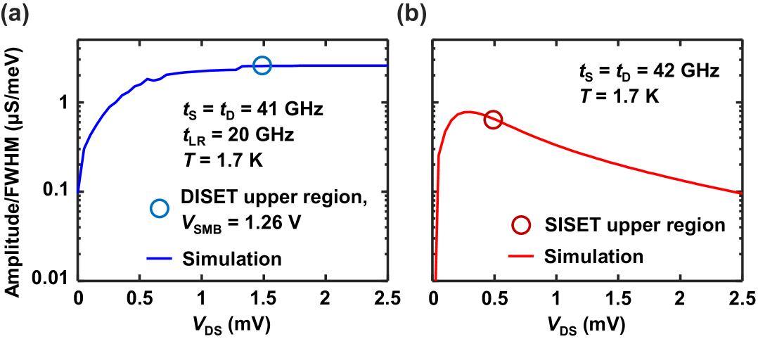
Lastly, the dependence of amplitude/FWHM on different source-drain bias is also simulated and plotted in Figure S4. We use the tunnel rates corresponding to the upper region of the DISET and the SISET, which are near-optimal. In Figure S4(a), we see that amplitude/FWHM of the DISET begins to saturate after mV. This agrees with our experimental observation that the increase in steepness is indistinct when is increased from 1 mV to 1.5 mV. Further increasing only creates larger bias triangles, which is beneficial for finding a sensitive point in charge sensing. Conversely, amplitude/FWHM of the SISET reaches a maximum at mV, followed by a slow decay. In the experiment, we applied a of mV, in close proximity to the optimal value.
E Output Noise Spectrum
The SNRs of both SETs experience a rapid decrease after kHz, which results in a faster increase of the readout error, especially for the DISET (which is more sensitive to all electric charge shifts, including noise). This can be explained by the noise spectrum shown in Figure S5. We plot the Welch power spectral density, which represents the noise distribution at different frequencies, on the same frequency scale as the plot of the SNR versus bandwidth. We see an increase in high frequency noise above kHz, which originates from the noise in the control setup or other environmental noise.
References
- Loss and DiVincenzo (1998) Daniel Loss and David P. DiVincenzo, “Quantum computation with quantum dots,” Physical Review A 57, 120–126 (1998).
- Kane (1998) B. E. Kane, “A silicon-based nuclear spin quantum computer,” Nature 393, 133–137 (1998).
- Morton et al. (2011) John J. L. Morton, Dane R. McCamey, Mark A. Eriksson, and Stephen A. Lyon, “Embracing the quantum limit in silicon computing,” Nature 479, 345–353 (2011).
- Zwanenburg et al. (2013) Floris A. Zwanenburg, Andrew S. Dzurak, Andrea Morello, Michelle Y. Simmons, Lloyd C. L. Hollenberg, Gerhard Klimeck, Sven Rogge, Susan N. Coppersmith, and Mark A. Eriksson, “Silicon quantum electronics,” Review of Modern Physics 85, 961–1019 (2013).
- Veldhorst et al. (2017) M. Veldhorst, H. G. J. Eenink, C. H. Yang, and A. S. Dzurak, “Silicon cmos architecture for a spin-based quantum computer,” Nature Communications 8, 1766 (2017).
- Vandersypen et al. (2017) L. M. K. Vandersypen, H. Bluhm, J. S. Clarke, A. S. Dzurak, R. Ishihara, A. Morello, D. J. Reilly, L. R. Schreiber, and M. Veldhorst, “Interfacing spin qubits in quantum dots and donors—hot, dense, and coherent,” npj Quantum Information 3, 34 (2017).
- Ladd and Carroll (2018) Thaddeus D. Ladd and Malcolm S. Carroll, “Silicon qubits,” Encyclopedia of Modern Optics (Second Edition) 1 (2018), 10.1016/B978-0-12-803581-8.09736-8.
- Gonzalez-Zalba et al. (2020) M. F. Gonzalez-Zalba, S. de Franceschi, E. Charbon, T. Meunier, M. Vinet, and A. S. Dzurak, “Scaling silicon-based quantum computing using cmos technology: State-of-the-art, challenges and perspectives,” (2020), arXiv:2011.11753 [quant-ph] .
- Jazaeri et al. (2019) F. Jazaeri, A. Beckers, A. Tajalli, and J. Sallese, “A review on quantum computing: From qubits to front-end electronics and cryogenic mosfet physics,” in 2019 MIXDES - 26th International Conference "Mixed Design of Integrated Circuits and Systems" (2019) pp. 15–25.
- Hornibrook et al. (2015) J. M. Hornibrook, J. I. Colless, I. D. Conway Lamb, S. J. Pauka, H. Lu, A. C. Gossard, J. D. Watson, G. C. Gardner, S. Fallahi, M. J. Manfra, and D. J. Reilly, “Cryogenic control architecture for large-scale quantum computing,” Physical Review Applied 3, 024010 (2015).
- Degenhardt et al. (2017) C. Degenhardt, L. Geck, A. Kruth, P. Vliex, and S. van Waasen, “Cmos based scalable cryogenic control electronics for qubits,” in 2017 IEEE International Conference on Rebooting Computing (ICRC) (2017) pp. 1–4.
- Bayer et al. (2019) Johannes C Bayer, Timo Wagner, Eddy P Rugeramigabo, and Rolf J Haug, “Charge reconfiguration in isolated quantum dot arrays,” Annalen der Physik 531, 1800393 (2019).
- Yang et al. (2020) C. H. Yang, R. C. C. Leon, J. C. C. Hwang, A. Saraiva, T. Tanttu, W. Huang, J. Camirand Lemyre, K. W. Chan, K. Y. Tan, F. E. Hudson, K. M. Itoh, A. Morello, M. Pioro-Ladrière, A. Laucht, and A. S. Dzurak, “Operation of a silicon quantum processor unit cell above one kelvin,” Nature 580, 350–354 (2020).
- Jones et al. (2018) Cody Jones, Michael A. Fogarty, Andrea Morello, Mark F. Gyure, Andrew S. Dzurak, and Thaddeus D. Ladd, “Logical qubit in a linear array of semiconductor quantum dots,” Physical Review X 8, 021058 (2018).
- Fogarty et al. (2018) M. A. Fogarty, K. W. Chan, B. Hensen, W. Huang, T. Tanttu, C. H. Yang, A. Laucht, M. Veldhorst, F. E. Hudson, K. M. Itoh, D. Culcer, T. D. Ladd, A. Morello, and A. S. Dzurak, “Integrated silicon qubit platform with single-spin addressability, exchange control and single-shot singlet-triplet readout,” Nature Communications 9, 4370 (2018).
- Zhao et al. (2019) R. Zhao, T. Tanttu, K. Y. Tan, B. Hensen, K. W. Chan, J. C. C. Hwang, R. C. C. Leon, C. H. Yang, W. Gilbert, F. E. Hudson, K. M. Itoh, A. A. Kiselev, T. D. Ladd, A. Morello, A. Laucht, and A. S. Dzurak, “Single-spin qubits in isotopically enriched silicon at low magnetic field,” Nature Communications 10, 5500 (2019).
- Seedhouse et al. (2021) Amanda E. Seedhouse, Tuomo Tanttu, Ross C.C. Leon, Ruichen Zhao, Kuan Yen Tan, Bas Hensen, Fay E. Hudson, Kohei M. Itoh, Jun Yoneda, Chih Hwan Yang, Andrea Morello, Arne Laucht, Susan N. Coppersmith, Andre Saraiva, and Andrew S. Dzurak, “Pauli blockade in silicon quantum dots with spin-orbit control,” Physical Review X Quantum 2, 010303 (2021).
- Petit et al. (2020) L. Petit, H. G. J. Eenink, M. Russ, W. I. L. Lawrie, N. W. Hendrickx, S. G. J. Philips, J. S. Clarke, L. M. K. Vandersypen, and M. Veldhorst, “Universal quantum logic in hot silicon qubits,” Nature 580, 355–359 (2020).
- Petit et al. (2018) L. Petit, J. M. Boter, H. G. J. Eenink, G. Droulers, M. L. V. Tagliaferri, R. Li, D. P. Franke, K. J. Singh, J. S. Clarke, R. N. Schouten, V. V. Dobrovitski, L. M. K. Vandersypen, and M. Veldhorst, “Spin lifetime and charge noise in hot silicon quantum dot qubits,” Physical Review Letter 121, 076801 (2018).
- Elzerman et al. (2004) J. M. Elzerman, R. Hanson, L. H. Willems van Beveren, L. M. K. Vandersypen, and L. P. Kouwenhoven, “Excited-state spectroscopy on a nearly closed quantum dot via charge detection,” Applied Physics Letters 84, 4617–4619 (2004).
- Yang et al. (2012) C. H. Yang, W. H. Lim, N. S. Lai, A. Rossi, A. Morello, and A. S. Dzurak, “Orbital and valley state spectra of a few-electron silicon quantum dot,” Physical Review B 86, 115319 (2012).
- Gotz et al. (2008) Georg Gotz, Gary A. Steele, Willem-Jan Vos, and Leo P. Kouwenhoven, “Real time electron tunneling and pulse spectroscopy in carbon nanotube quantum dots,” Nano Letters 8, 4039–4042 (2008).
- Fowler et al. (2009) Austin G. Fowler, Ashley M. Stephens, and Peter Groszkowski, “High-threshold universal quantum computation on the surface code,” Physical Review A 80, 052312 (2009).
- Fowler et al. (2012) Austin G. Fowler, Matteo Mariantoni, John M. Martinis, and Andrew N. Cleland, “Surface codes: Towards practical large-scale quantum computation,” Physical Review A 86, 032324 (2012).
- Knill (2005) E. Knill, “Quantum computing with realistically noisy devices,” Nature 434, 39–44 (2005).
- Lim et al. (2009a) W. H. Lim, H. Huebl, L. H. Willems van Beveren, S. Rubanov, P. G. Spizzirri, S. J. Angus, R. G. Clark, and A. S. Dzurak, “Electrostatically defined few-electron double quantum dot in silicon,” Applied Physics Letters 94, 173502 (2009a).
- Lim et al. (2009b) W. H. Lim, F. A. Zwanenburg, H. Huebl, M. Möttönen, K. W. Chan, A. Morello, and A. S. Dzurak, “Observation of the single-electron regime in a highly tunable silicon quantum dot,” Applied Physics Letters 95, 242102 (2009b).
- Angus et al. (2007) Susan J. Angus, Andrew J. Ferguson, Andrew S. Dzurak, and Robert G. Clark, “Gate-defined quantum dots in intrinsic silicon,” Nano Letters 7, 2051–2055 (2007).
- van der Wiel et al. (2002) W. G. van der Wiel, S. De Franceschi, J. M. Elzerman, T. Fujisawa, S. Tarucha, and L. P. Kouwenhoven, “Electron transport through double quantum dots,” Review of Modern Physics 75, 1–22 (2002).
- Fujisawa et al. (1998) Toshimasa Fujisawa, Tjerk H. Oosterkamp, Wilfred G. van der Wiel, Benno W. Broer, Ramón Aguado, Seigo Tarucha, and Leo P. Kouwenhoven, “Spontaneous emission spectrum in double quantum dot devices,” Science 282, 932–935 (1998).
- Medford et al. (2013) J. Medford, J. Beil, J. M. Taylor, S. D. Bartlett, A. C. Doherty, E. I. Rashba, D. P. DiVincenzo, H. Lu, A. C. Gossard, and C. M. Marcus, “Self-consistent measurement and state tomography of an exchange-only spin qubit,” Nature Nanotechnology 8, 654–659 (2013).
- Stoof and Nazarov (1996) T. H. Stoof and Yu. V. Nazarov, “Time-dependent resonant tunneling via two discrete states,” Physical Review B 53, 1050–1053 (1996).
- Wang et al. (2013) K. Wang, C. Payette, Y. Dovzhenko, P. W. Deelman, and J. R. Petta, “Charge relaxation in a single-electron double quantum dot,” Physical Review Letter 111, 046801 (2013).
- Ihn (2015) Thomas Ihn, Semiconductor nanostructures (Oxford University Press, 2015) p. 395.
- Yang et al. (2011) C. H. Yang, W. H. Lim, F. A. Zwanenburg, and A. S. Dzurak, “Dynamically controlled charge sensing of a few-electron silicon quantum dot,” AIP Advances 1, 042111 (2011).
- Eenink et al. (2019) H. G. J. Eenink, L. Petit, W. I. L. Lawrie, J. S. Clarke, L. M. K. Vandersypen, and M. Veldhorst, “Tunable coupling and isolation of single electrons in silicon metal-oxide-semiconductor quantum dots,” Nano Letters 19, 8653–8657 (2019).
- Huang et al. (2019) W. Huang, C. H. Yang, K. W. Chan, T. Tanttu, B. Hensen, R. C. C. Leon, M. A. Fogarty, J. C. C. Hwang, F. E. Hudson, K. M. Itoh, A. Morello, A. Laucht, and A. S. Dzurak, “Fidelity benchmarks for two-qubit gates in silicon,” Nature 569, 532–536 (2019).
- Veldhorst et al. (2015) M. Veldhorst, C. H. Yang, J. C. C. Hwang, W. Huang, J. P. Dehollain, J. T. Muhonen, S. Simmons, A. Laucht, F. E. Hudson, K. M. Itoh, A. Morello, and A. S. Dzurak, “A two-qubit logic gate in silicon,” Nature 526, 410–414 (2015).
- Veldhorst et al. (2014) M. Veldhorst, J. C. C. Hwang, C. H. Yang, A. W. Leenstra, B. de Ronde, J. P. Dehollain, J. T. Muhonen, F. E. Hudson, K. M. Itoh, A. Morello, and et al., “An addressable quantum dot qubit with fault-tolerant control-fidelity,” Nature Nanotechnology 9, 981–985 (2014).
- Brauns et al. (2018) Matthias Brauns, Sergey V. Amitonov, Paul-Christiaan Spruijtenburg, and Floris A. Zwanenburg, “Palladium gates for reproducible quantum dots in silicon,” Scientific Reports 8, 5690 (2018).
- Lai et al. (2011) N. S. Lai, W. H. Lim, C. H. Yang, F. A. Zwanenburg, W. A. Coish, F. Qassemi, A. Morello, and A. S. Dzurak, “Pauli spin blockade in a highly tunable silicon double quantum dot,” Scientific Reports 1, 110 (2011).
- Hubbard and Flowers (1963) J. Hubbard and Brian Hilton Flowers, “Electron correlations in narrow energy bands,” Proceedings of the Royal Society of London. Series A. Mathematical and Physical Sciences 276, 238–257 (1963).
- Das Sarma et al. (2011) S. Das Sarma, Xin Wang, and Shuo Yang, “Hubbard model description of silicon spin qubits: Charge stability diagram and tunnel coupling in si double quantum dots,” Physical Review B 83, 235314 (2011).
- Wang et al. (2011) Xin Wang, Shuo Yang, and S. Das Sarma, “Quantum theory of the charge-stability diagram of semiconductor double-quantum-dot systems,” Physical Review B 84, 115301 (2011).
- Lindblad (1976) G. Lindblad, “On the generators of quantum dynamical semigroups,” Communications in Mathematical Physics 48, 119–130 (1976).
- Gorini et al. (1976) Vittorio Gorini, Andrzej Kossakowski, and E. C. G. Sudarshan, “Completely positive dynamical semigroups of n-level systems,” Journal of Mathematical Physics 17, 821–825 (1976).
- Gurvitz and Prager (1996) S. A. Gurvitz and Ya. S. Prager, “Microscopic derivation of rate equations for quantum transport,” Physical Review B 53, 15932–15943 (1996).
- Gurvitz et al. (1996) S.A. Gurvitz, H.J. Lipkin, and Ya.S. Prager, “Interference effects in resonant tunneling and the pauli principle,” Physics Letters A 212, 91–96 (1996).
- Touati et al. (2014) Amine Touati, Samir Chatbouri, Nabil Sghaier, and Adel Kalboussi, “Theoretical analysis and characterization of multi-islands single-electron devices with applications,” The Scientific World Journal 2014, 241214 (2014).
- Chao Zhang et al. (2010) Chao Zhang, Liang Fang, Bingcai Sui, Yaqing Chi, and Sorin Dan Cotofana, “A master equation model of multi-island single-electron transistors based on stability diagram,” in 2010 2nd International Conference on Computer Engineering and Technology, Vol. 3 (2010) pp. V3–227–V3–231.
- Boubaker et al. (2009) A. Boubaker, M. Troudi, Na. Sghaier, A. Souifi, N. Baboux, and A. Kalboussi, “Electrical characteristics and modelling of multi-island single-electron transistor using simon simulator,” Microelectronics Journal 40, 543 – 546 (2009), workshop of Recent Advances on Low Dimensional Structures and Devices (WRA-LDSD).
- Brenner (2004) Rolf Brenner, Single-electron transistors for detection of charge motion in the solid state (University of New South Wales, 2004).
- Hovhannisyan and Imparato (2019) Karen V Hovhannisyan and Alberto Imparato, “Quantum current in dissipative systems,” New Journal of Physics 21, 052001 (2019).