A telecom O-band emitter in diamond
Abstract
Color centers in diamond are promising platforms for quantum technologies. Most color centers in diamond discovered thus far emit in the visible or near-infrared wavelength range, which are incompatible with long-distance fiber communication and unfavorable for imaging in biological tissues. Here, we report the experimental observation of a new color center that emits in the telecom O-band, which we observe in silicon-doped bulk single crystal diamonds and microdiamonds. Combining absorption and photoluminescence measurements, we identify a zero-phonon line at 1221 nm and phonon replicas separated by 42 meV. Using transient absorption spectroscopy, we measure an excited state lifetime of around 270 ps and observe a long-lived baseline that may arise from intersystem crossing to another spin manifold.
Quantum emitters are widely explored for quantum technologies [1, 2, 3, 4], particularly quantum communication and quantum sensing applications [5, 6]. For quantum communication, transmission over long distances requires the use of existing fiber-based optical communication networks [7] where losses are high in the visible and near-infrared region. For comparison, visible light can undergo a fiber loss of 8 dB/km, whereas it is about 0.5 dB/km at 1300 nm and 0.2 dB/km at 1550 nm [8]. For sensing applications, the second near-infrared (NIR-II) window spanning 1000-1700 nm is particularly attractive for biological imaging because of deeper optical penetration, lower absorption and higher contrast due to reduced background autofluorescence and scattering from biological tissues [9].
Some of the most widely studied quantum emitters are color centers in diamond [10, 11, 12], namely the nitrogen vacancy (NV-) [13, 14], negative silicon vacancy (SiV-) [15, 16, 17, 18] and neutral silicon vacancy (SiV0) [19, 20] centers, all of which emit photons in the visible to near-infrared region. To date, a few defects in other host materials have been reported that emit in the telecom band: the G-, T- and W-centers in silicon [21, 22, 23], NV-, vanadium, and molybdenum in silicon carbide [24, 25, 26], and erbium in various host materials [27, 28, 29, 30, 31], but no color centers in diamond have been reported in the telecom band. Diamond offers several unique advantages as a host – it has a large optical transparency window, has the highest Debye temperature of any material, is chemically inert and biocompatible, and can provide a low magnetic noise environment with the low natural abundance of 13C [11]. Hence, there is significant motivation to search for telecom band emitters in diamond.
Here, we report the experimental observation of an emitter in diamond that emits at 1221 nm, which is near the ‘original’ wavelength band (O-band) used for optical communication. Using photoluminescence (PL) and absorption spectroscopy, we identify a zero-phonon line (ZPL) at 1221 nm and phonon replicas spaced by 42 meV. Using transient absorption spectroscopy, we probe the excited state lifetime of the defect and also observe a long-lived shelving state. We tentatively assign this defect as a silicon-related defect, and we compare it to prior theoretical reports [32].
The samples studied in this work are silicon doped samples with different form factors and synthesis conditions, from bulk diamonds to microdiamonds and nanodiamonds. The three bulk diamonds (labelled samples 1, 2, and 3) were grown by plasma chemical vapor deposition (CVD, Element Six) and doped with silicon during growth [33]. These contain ensembles of SiV0, and optical and spin characterization of SiV0 in sample 1 were reported in Ref. 34, 20. Silicon-doped microdiamonds were made using high-pressure high-temperature (HPHT) synthesis (Hyperion Materials & Technologies), followed by bead milling to reduce the size of the as-synthesized crystals. Nanodiamond particles were extracted from this sample using centrifugation [33]. The microdiamonds have been reported to exhibit fluorescence from silicon-related defects including SiV- and silicon-boron color centers [35], and we also observe PL from SiV0 (Fig. S6 [33]). In our study, broadband absorption measurement was conducted using a UV-Vis-NIR spectrophotometer (Agilent, Cary 5000) at room temperature. Low temperature optical measurements were performed in home-built confocal microscopes equipped with 850 nm optical excitation and a spectrometer with a liquid nitrogen cooled InGaAs detector (PyLoN IR, Princeton Instruments). Transient absorption measurements were conducted using a femtosecond, broadband transient absorption spectrometer [36] (Helios, Ultrafast Systems) with the sample cooled to 4.2 K.
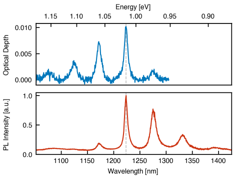
First, we probe the telecom band emitter by correlating absorption and PL measurements on a bulk CVD diamond, sample 1, at room temperature (Fig. 1). Using 850 nm excitation, we observe several PL peaks at 1173 nm, 1224 nm, 1276 nm, 1332 nm, and 1393 nm that are evenly spaced and separated by approximately 42 meV. Absorption spectroscopy reveals similar evenly spaced peaks at 1076 nm, 1124 nm, 1172 nm, 1224 nm, and 1275 nm, consistent with prior observations of absorption lines in these bands in silicon doped diamond [37]. The absorption and PL spectra display a clear mirror symmetry with the symmetry axis being the most intense peak at 1224 nm (1.0129 eV). The symmetry between absorption and emission suggests the peaks originate from the same defect, with a ZPL at 1224 nm.
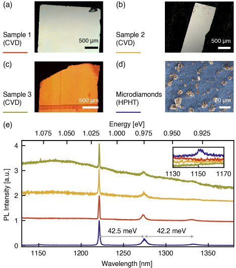
With the assignment of the absorption and emission peaks to a common defect, we probe its optical properties at cryogenic temperatures. We measure the emission spectrum from 1100 nm to 1400 nm using 850 nm excitation on the three bulk silicon doped samples (Fig. 2(a), (b) and (c)) and silicon doped microdiamonds (Fig. 2(d)). Despite their drastically different form factors, synthesis conditions, and preparation methods, we observe three evenly spaced PL peaks (1221 nm, 1273 nm, and 1330 nm) common to all samples (Fig. 2(e)). The peak at 1221 nm shows the narrowest linewidth among the three peaks, consistent with it being the ZPL. Additional features such as a broad background in samples 2 and 3 and an additional peak at 1152 nm in the microdiamonds are observable, but they do not correlate across samples, indicating they are not related to the same defect. We can also observe the 1221 nm transition in silicon doped sub-100 nm nanodiamonds, although with a much lower emission intensity (Fig. S2 [33]). The spacing (42 meV) between the peaks is consistent with theoretical calculations of the localized vibronic mode arising from the vibration of a silicon atom in various silicon containing complexes [32]. Based on this observation, together with the abundance of silicon in these samples, we hypothesize that the 1221 nm emission arises from a silicon-related defect. We note that all the diamonds in which we have observed the telecom emitter also contain SiV0, which may suggest that its charge transition energy is near the valence band maximum. The microscopic nature of this defect requires further investigation but absorption lines in this band were proposed to arise from SiV2:H(-) in a recent theoretical study [32].
Comparing the room temperature and low temperature spectra, we observe that the emission peak at 1170 nm is present at room temperature but not at low temperature (Fig. 3(a)). Hence, we investigate the optical properties of the telecom emitter by studying the temperature dependence of the PL spectra in detail. At temperatures higher than 90 K, the peak at 1170 nm becomes visible (Fig. S3(a)). The ratio of the intensity of the 1170 nm peak compared to the ZPL follows an exponential temperature dependence (Fig. 3(b)). By fitting the ratio of intensities with , we obtain an activation energy of meV, consistent with the separation between the 1170 nm peak and the ZPL (44.9 meV at 295 K). The occurrence of this higher energy peak and its exponential activation with temperature are consistent across multiple samples (microdiamonds: Fig. 3(b), sample 1: Fig. S3(c)). Therefore, we attribute this 1170 nm peak to the emission of a photon from a vibrational excited state in the electronic excited state manifold. We note that we do not observe a uniform trend for the temperature dependence of the total PL intensity across different samples, which may be related to defect-defect interactions and charge state dynamics.
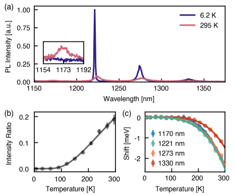
At higher temperatures, the PL peak positions shift to longer wavelengths and the linewidths broaden. For comparison, the linewidth at 6.2 K for the microdiamonds is nm, whereas the room temperature linewidth is nm. The magnitude of the shift is similar to previous reports for NV [38, 39] and SiV- [40] centers, where the shifts were attributed to the expansion of the diamond lattice along with temperature-dependent electron-phonon interactions. The volume expansion coefficient of diamond has been empirically shown to have a cubic dependence on temperature [41], which causes the lattice expansion to contribute a term to the energy shift. This, combined with the softening of elastic bonds in the excited states [38], leads to a dependence (sample 1: Fig. 3(c), microdiamonds: Fig. S3(b) [33]).
To study the optical dynamics of the defect, we perform pump-probe measurements using transient absorption spectroscopy on sample 1. We apply a femtosecond 937 nm pump pulse (FWHM 16 nm, photons/cm2, Fig. S1 [33]) to excite the ground state population and use a broadband (820-1350 nm) probe pulse to monitor the change in absorption after the pump. The repetition rate for the sequence is kept at 1 kHz to ensure full relaxation of the population in the beginning of each sequence. The difference in absorption, , with and without the pump is measured at different pump-probe time separations (Fig. 4(a)). Within the spectrum, we observe minima that are consistent with the steady-state absorption spectrum (Fig. 1) and match with the peak positions in the PL spectra (Fig. 4(b)).
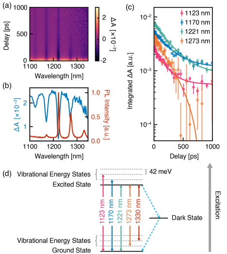
The nature of these minima depends on their relative position to the ZPL. The higher energy dips (1123 nm, 1170 nm) arise from absorption from the ground state to different vibrational states in the excited state. They appear as minima in the spectrum (Fig. 4(b)) because the ground state population is bleached by the pump, leading to less absorption of the probe pulse. The appearance of the lower energy dip at 1273 nm is inconsistent with the absorption process at 4.2 K, as it would require the thermal population of a vibrationally excited mode (42 meV) in the ground state, which is a much larger energy than the thermal energy (0.36 meV). Instead, this feature at 1273 nm is likely the result of stimulated emission [42], where the excited state is first populated after the pump and then emission is stimulated with the probe, creating a dip in . Similarly, the dip at the ZPL can have contributions from both ground state bleach and stimulated emission.
The temporal dependence of reveals the kinetics of the population dynamics. We observe exponential decays for the integrated at each band (Fig. 4(c)). The decay constant for the different peaks are similar (around 270 ps), suggesting they share the same decay paths. The decay of for the 1273 nm dip is attributed to the decay of the excited state population. Therefore, we infer the lifetime of this emitter to be ps. We note that sample 1 also shows signs of charge state conversion between the telecom emitter and SiV0 (Fig. S6 [33]), which may affect the measured lifetime in this sample. We observe different baselines for the different bands. The decay for the 1273 nm transition reaches a value of zero, suggesting all the population from the excited state is relaxed. However, the curves for 1123 nm, 1170 nm and 1221 nm decay to a non-zero baseline, suggesting that the ground state population is trapped in a dark shelving state with a lifetime much longer than the duration of the measurement (1 ns).
Combining PL, absorption, and transient absorption, we propose a tentative level structure for this telecom emitter (Fig. 4(d)). The emission band at 1221 nm is assigned to the ZPL because it is the mirror axis of absorption and emission spectra. The defect has a silicon-related vibrational mode with an energy of 42 meV. The population of this mode in the excited state leads to the anti-Stokes lines at 1170 nm and 1123 nm, while the population of this mode in the ground state leads to the Stokes lines at 1273 nm and 1330 nm. Finally, we propose the existence of an additional dark state with longer lifetime coupled to the optically active states through an intersystem crossing. We note that this level structure resembles the level structure of its proposed SiV2:H(-) assignment [32]. For SiV2:H(-), the level structure was proposed to have a singlet-to-singlet optical transition with a triplet shelving state. We carried out additional calculations on this model which further strengthen the tentative assignment of the center to the SiV2:H(-) defect model. We find that the short PL lifetime originates from the fast non-radiative decay from the singlet excited state to the singlet ground state [33].
To summarize, we have experimentally observed telecom O-band PL emission from a silicon-related defect in CVD and HPHT diamonds. A tentative level structure is proposed based on PL emission, absorption, and transient absorption. More experimental investigations are required to confirm its microscopic structure and symmetry. In order to confirm the defect structure, silicon ion implantation followed by hydrogen diffusion and annealing could be used to form silicon containing centers decorated with hydrogen [43, 44]. In addition to longer propagation lengths in optical fiber, the telecom band emission wavelength leads to reduced scattering in nanophotonic devices [45], allowing for more efficient integration for long distance quantum networks. Furthermore, diamond nanoparticles hosting the telecom emitter can be potentially incorporated as bioimaging probes by virtue of their form factor and emission in the NIR-II window.
This work was primarily supported by the U.S. Department of Energy, Office of Science, National Quantum Information Science Research Centers, Co-design Center for Quantum Advantage (C2QA) under contract number DE-SC0012704. Ultrafast measurements and materials characterization were performed with support from the Air Force Office of Scientific Research under Grant No. FA9550-17-0158. This research was also supported by the Australian Research Council Center of Excellence for Nanoscale BioPhotonics (No. CE140100003) and the Australian Research Council Center of Excellence for Quantum Computation and Communication Technology (No. CE170100012). P.R. acknowledges funding through the RMIT Vice-Chancellor’s Research Fellowship and ARC DECRA Fellowship scheme (No. DE200100279). M.dV. acknowledges funding through the RMIT’s Research Stipend Scholarship (RRSS-SC). The authors acknowledge the use of the RMIT Microscopy and Microanalysis Facility (RMMF) at RMIT University. Á. G. acknowledges the support from the NKFIH in Hungary for the National Excellence Program (Grant No. KKP129866), the Quantum Information National Laboratory, and the EU QuantERA II Sensextreme project. G. T. was supported by the János Bolyai Research Scholarship of the Hungarian Academy of Sciences. G. T. acknowledges the high-performance computational resources provided by KIFÜ (Governmental Agency for IT Development) institute of Hungary.
References
- O’brien et al. [2009] J. L. O’brien, A. Furusawa, and J. Vučković, Photonic quantum technologies, Nature Photonics 3, 687 (2009).
- Buluta et al. [2011] I. Buluta, S. Ashhab, and F. Nori, Natural and artificial atoms for quantum computation, Reports on Progress in Physics 74, 104401 (2011).
- Azzam et al. [2021] S. I. Azzam, K. Parto, and G. Moody, Prospects and challenges of quantum emitters in 2d materials, Applied Physics Letters 118, 240502 (2021).
- de Leon et al. [2021] N. P. de Leon, K. M. Itoh, D. Kim, K. K. Mehta, T. E. Northup, H. Paik, B. Palmer, N. Samarth, S. Sangtawesin, and D. Steuerman, Materials challenges and opportunities for quantum computing hardware, Science 372, eabb2823 (2021).
- Atatüre et al. [2018] M. Atatüre, D. Englund, N. Vamivakas, S.-Y. Lee, and J. Wrachtrup, Material platforms for spin-based photonic quantum technologies, Nature Reviews Materials 3, 38 (2018).
- Awschalom et al. [2018] D. D. Awschalom, R. Hanson, J. Wrachtrup, and B. B. Zhou, Quantum technologies with optically interfaced solid-state spins, Nature Photonics 12, 516 (2018).
- Cao et al. [2019] X. Cao, M. Zopf, and F. Ding, Telecom wavelength single photon sources, Journal of Semiconductors 40, 071901 (2019).
- Agrawal [2012] G. P. Agrawal, Fiber-optic communication systems (John Wiley & Sons, 2012).
- Duan and Liu [2018] Y. Duan and B. Liu, Recent advances of optical imaging in the second near-infrared window, Advanced materials 30, 1802394 (2018).
- Ruf et al. [2021] M. Ruf, N. H. Wan, H. Choi, D. Englund, and R. Hanson, Quantum networks based on color centers in diamond, Journal of Applied Physics 130, 070901 (2021).
- Pezzagna and Meijer [2021] S. Pezzagna and J. Meijer, Quantum computer based on color centers in diamond, Applied Physics Reviews 8, 011308 (2021).
- Rodgers et al. [2021] L. V. Rodgers, L. B. Hughes, M. Xie, P. C. Maurer, S. Kolkowitz, A. C. Bleszynski Jayich, and N. P. de Leon, Materials challenges for quantum technologies based on color centers in diamond, MRS Bulletin 46, 623 (2021).
- Maletinsky et al. [2012] P. Maletinsky, S. Hong, M. S. Grinolds, B. Hausmann, M. D. Lukin, R. L. Walsworth, M. Loncar, and A. Yacoby, A robust scanning diamond sensor for nanoscale imaging with single nitrogen-vacancy centres, Nature nanotechnology 7, 320 (2012).
- Bernien et al. [2013] H. Bernien, B. Hensen, W. Pfaff, G. Koolstra, M. S. Blok, L. Robledo, T. H. Taminiau, M. Markham, D. J. Twitchen, L. Childress, et al., Heralded entanglement between solid-state qubits separated by three metres, Nature 497, 86 (2013).
- Rogers et al. [2014] L. J. Rogers, K. D. Jahnke, M. H. Metsch, A. Sipahigil, J. M. Binder, T. Teraji, H. Sumiya, J. Isoya, M. D. Lukin, P. Hemmer, et al., All-optical initialization, readout, and coherent preparation of single silicon-vacancy spins in diamond, Physical review letters 113, 263602 (2014).
- Pingault et al. [2017] B. Pingault, D.-D. Jarausch, C. Hepp, L. Klintberg, J. N. Becker, M. Markham, C. Becher, and M. Atatüre, Coherent control of the silicon-vacancy spin in diamond, Nature communications 8, 1 (2017).
- Nguyen et al. [2019a] C. Nguyen, D. Sukachev, M. Bhaskar, B. Machielse, D. Levonian, E. Knall, P. Stroganov, C. Chia, M. Burek, R. Riedinger, et al., An integrated nanophotonic quantum register based on silicon-vacancy spins in diamond, Physical Review B 100, 165428 (2019a).
- Nguyen et al. [2019b] C. Nguyen, D. Sukachev, M. Bhaskar, B. Machielse, D. Levonian, E. Knall, P. Stroganov, R. Riedinger, H. Park, M. Lončar, et al., Quantum network nodes based on diamond qubits with an efficient nanophotonic interface, Physical review letters 123, 183602 (2019b).
- Rose et al. [2018a] B. C. Rose, D. Huang, Z.-H. Zhang, P. Stevenson, A. M. Tyryshkin, S. Sangtawesin, S. Srinivasan, L. Loudin, M. L. Markham, A. M. Edmonds, et al., Observation of an environmentally insensitive solid-state spin defect in diamond, Science 361, 60 (2018a).
- Zhang et al. [2020] Z.-H. Zhang, P. Stevenson, G. Thiering, B. C. Rose, D. Huang, A. M. Edmonds, M. L. Markham, S. A. Lyon, A. Gali, and N. P. De Leon, Optically detected magnetic resonance in neutral silicon vacancy centers in diamond via bound exciton states, Physical Review Letters 125, 237402 (2020).
- Udvarhelyi et al. [2021] P. Udvarhelyi, B. Somogyi, G. Thiering, and A. Gali, Identification of a telecom wavelength single photon emitter in silicon, Physical Review Letters 127, 196402 (2021).
- Safonov et al. [1996] A. Safonov, E. Lightowlers, G. Davies, P. Leary, R. Jones, and S. Öberg, Interstitial-carbon hydrogen interaction in silicon, Physical review letters 77, 4812 (1996).
- Baron et al. [2022] Y. Baron, A. Durand, P. Udvarhelyi, T. Herzig, M. Khoury, S. Pezzagna, J. Meijer, I. Robert-Philip, M. Abbarchi, J.-M. Hartmann, et al., Detection of single w-centers in silicon, ACS Photonics 9, 2337 (2022).
- Zargaleh et al. [2018] S. A. Zargaleh, S. Hameau, B. Eble, F. Margaillan, H. J. von Bardeleben, J.-L. Cantin, and W. Gao, Nitrogen vacancy center in cubic silicon carbide: A promising qubit in the 1.5 m spectral range for photonic quantum networks, Physical Review B 98, 165203 (2018).
- Wolfowicz et al. [2020] G. Wolfowicz, C. P. Anderson, B. Diler, O. G. Poluektov, F. J. Heremans, and D. D. Awschalom, Vanadium spin qubits as telecom quantum emitters in silicon carbide, Science advances 6, eaaz1192 (2020).
- Bosma et al. [2018] T. Bosma, G. J. Lof, C. M. Gilardoni, O. V. Zwier, F. Hendriks, B. Magnusson, A. Ellison, A. Gällström, I. G. Ivanov, N. Son, et al., Identification and tunable optical coherent control of transition-metal spins in silicon carbide, npj Quantum Information 4, 1 (2018).
- Yin et al. [2013] C. Yin, M. Rancic, G. G. de Boo, N. Stavrias, J. C. McCallum, M. J. Sellars, and S. Rogge, Optical addressing of an individual erbium ion in silicon, Nature 497, 91 (2013).
- Alizadehkhaledi et al. [2019] A. Alizadehkhaledi, A. L. Frencken, F. C. van Veggel, and R. Gordon, Isolating nanocrystals with an individual erbium emitter: A route to a stable single-photon source at 1550 nm wavelength, Nano Letters 20, 1018 (2019).
- Raha et al. [2020] M. Raha, S. Chen, C. M. Phenicie, S. Ourari, A. M. Dibos, and J. D. Thompson, Optical quantum nondemolition measurement of a single rare earth ion qubit, Nature communications 11, 1 (2020).
- Dibos et al. [2018] A. Dibos, M. Raha, C. Phenicie, and J. D. Thompson, Atomic source of single photons in the telecom band, Physical review letters 120, 243601 (2018).
- Cajzl et al. [2017] J. Cajzl, P. Nekvindová, A. Macková, P. Malinskỳ, D. Sedmidubskỳ, M. Hušák, Z. Remeš, M. Varga, A. Kromka, R. Böttger, et al., Erbium ion implantation into diamond–measurement and modelling of the crystal structure, Physical Chemistry Chemical Physics 19, 6233 (2017).
- Thiering and Gali [2015] G. Thiering and A. Gali, Complexes of silicon, vacancy, and hydrogen in diamond: A density functional study, Physical Review B 92, 165203 (2015).
- [33] See Supplemental Material for experimental methods, additional characterization data and discussions.
- Rose et al. [2018b] B. C. Rose, G. Thiering, A. M. Tyryshkin, A. M. Edmonds, M. L. Markham, A. Gali, S. A. Lyon, and N. P. de Leon, Strongly anisotropic spin relaxation in the neutral silicon vacancy center in diamond, Physical Review B 98, 235140 (2018b).
- Shames et al. [2020] A. I. Shames, A. Dalis, A. D. Greentree, B. C. Gibson, H. Abe, T. Ohshima, O. Shenderova, A. Zaitsev, and P. Reineck, Near-infrared fluorescence from silicon-and nickel-based color centers in high-pressure high-temperature diamond micro-and nanoparticles, Advanced Optical Materials 8, 2001047 (2020).
- Pensack et al. [2016] R. D. Pensack, E. E. Ostroumov, A. J. Tilley, S. Mazza, C. Grieco, K. J. Thorley, J. B. Asbury, D. S. Seferos, J. E. Anthony, and G. D. Scholes, Observation of two triplet-pair intermediates in singlet exciton fission, The journal of physical chemistry letters 7, 2370 (2016).
- D’Haenens-Johansson [2011] U. F. D’Haenens-Johansson, Optical and Magnetic Resonance Studies of Point Defects in CVD Diamond, Ph.D. thesis, University of Warwick (2011).
- Hizhnyakov et al. [2002] V. Hizhnyakov, H. Kaasik, and I. Sildos, Zero-phonon lines: the effect of a strong softening of elastic springs in the excited state, physica status solidi (b) 234, 644 (2002).
- Davies [1974] G. Davies, Vibronic spectra in diamond, Journal of Physics C: Solid State Physics 7, 3797 (1974).
- Neu et al. [2013] E. Neu, C. Hepp, M. Hauschild, S. Gsell, M. Fischer, H. Sternschulte, D. Steinmüller-Nethl, M. Schreck, and C. Becher, Low-temperature investigations of single silicon vacancy colour centres in diamond, New Journal of Physics 15, 043005 (2013).
- Stoupin and Shvyd’ko [2011] S. Stoupin and Y. V. Shvyd’ko, Ultraprecise studies of the thermal expansion coefficient of diamond using backscattering x-ray diffraction, Physical Review B 83, 104102 (2011).
- Berera et al. [2009] R. Berera, R. van Grondelle, and J. Kennis, Ultrafast transient absorption spectroscopy: principles and application to photosynthetic systems, Photosynthesis research 101, 105 (2009).
- Glover et al. [2003] C. Glover, M. Newton, P. Martineau, D. Twitchen, and J. Baker, Hydrogen incorporation in diamond: The nitrogen-vacancy-hydrogen complex, Physical review letters 90, 185507 (2003).
- Fuchs et al. [1995] F. Fuchs, C. Wild, K. Schwarz, W. Müller-Sebert, and P. Koidl, Hydrogen induced vibrational and electronic transitions in chemical vapor deposited diamond, identified by isotopic substitution, Applied Physics Letters 66, 177 (1995).
- Burek et al. [2014] M. J. Burek, Y. Chu, M. S. Liddy, P. Patel, J. Rochman, S. Meesala, W. Hong, Q. Quan, M. D. Lukin, and M. Lončar, High quality-factor optical nanocavities in bulk single-crystal diamond, Nature communications 5, 1 (2014).