AlGaAs/GaAs single electron transistors fabricated without modulation doping
Abstract
We have fabricated quantum dot single electron transistors, based on AlGaAs/GaAs heterojunctions without modulation doping, which exhibit clear and stable Coulomb blockade oscillations. The temperature dependence of the Coulomb blockade peak lineshape is well described by standard Coulomb blockade theory in the quantum regime. Bias spectroscopy measurements have allowed us to directly extract the charging energy, and showed clear evidence of excited state transport, confirming that individual quantum states in the dot can be resolved.
Quantum dots are central to nanoelectronics and have been used to realize single-electron transistors (SETs), Meirav:1990prl artificial atoms, Kastner:1993phystod ultra-sensitive electrometers, Fujisawa:2004apl and may ultimately be used as elements for quantum information applications. Loss:1998pra ; Hanson:2007rmp Semiconductor quantum dots are typically defined using negatively-biased surface gates to deplete regions of the two-dimensional electron gas (2DEG) formed in a modulation-doped AlGaAs/GaAs heterostructure. Kouwenhoven:1997nato Although modulation doping results in high electron mobilities, Dingle:1978apl it can also cause significant charge noise and temporal instability due to rapid switching of the dopants between ionized and de-ionized states. Kurdak:1997prb ; Pioro-Ladriere:2005prb ; Buizert:2008prl Methods such as cooling the device with the gates biased Pioro-Ladriere:2005prb or depositing gates on a thin insulating layer Buizert:2008prl can reduce charge noise but not eliminate it entirely, hindering the development of ultra-sensitive quantum devices.
Here we report the development of a quantum dot in a heterostructure without modulation doping. Instead the electron gas is ‘induced’ electrostatically using a degenerately doped metallic top-gate in an otherwise undoped heterostructure. Kane:1995apl The present device architecture overcomes many of the limitations of the inverted semiconductor-insulator-semiconductor (ISIS) heterostructure used in some of the earliest studies of GaAs SETs. Meirav:1990prl In the ISIS device, a heavily-doped substrate was used as a gate to induce a 2DEG at an inverted AlGaAs/GaAs interface, with the quantum dot defined by negatively-biased Schottky gates. However, the ISIS heterostructure also has a delta-doped layer between the Schottky gates and the 2DEG to counter GaAs surface states, leading to similar disorder to modulation-doped heterostructures. Meirav:1990thesis ISIS devices also suffer from the reduced mobility inherent in inverted interfaces, Heiblum:1985jvstb and ohmic contact penetration into the doped substrate. Meirav:1990thesis Our device overcomes these problems – there is no need for shallow ohmic contacts, no inverted interface, and although we use a doped cap layer as a gate, it is degenerately doped to have a metallic conductivity at low temperature, providing a sufficiently high electron density to screen the 2DEG from ionized donors in the cap. With this device we observe clean and stable Coulomb blockade oscillations, and single particle states within the dot.
Our devices were fabricated from an AlGaAs/GaAs heterostructure consisting of (from undoped GaAs buffer upwards): a nm undoped AlGaAs barrier, a nm GaAs spacer, and a nm n+-GaAs cap used as a metallic gate. Hall bars with annealed NiGeAu ohmic contacts are defined using a self-aligned process. Kane:1995apl The 2DEG is depleted at top gate bias V, and above this threshold, the electron density cm-2. Characterization of the heterostructure gave a mobility of cmVs at cm-2. A quantum dot with dimensions m was defined by using electron beam lithography and a H2SO4 etch to form a nm deep trench dividing the cap into seven separate gates, as shown in Fig. 1(c). The quantum dot and adjacent 2DEG reservoirs are populated using the top gate. At each end is a quantum point contact (QPC) defined by split-gates biased at and , which control the tunnel barriers between the dot and the reservoirs (both QPCs are set with a conductance less than ). Finally, the bottom ‘plunger gate’, biased at , allows the occupancy of the dot to be tuned (the upper plunger gate was connected to ground for the entire experiment). Electrical measurements were performed using ac and dc techniques with the dot cooled to millikelvin temperatures by a dilution refrigerator. The temperature was measured using a Nanoway cryoelectronics primary Coulomb blockade thermometer mounted with the device.
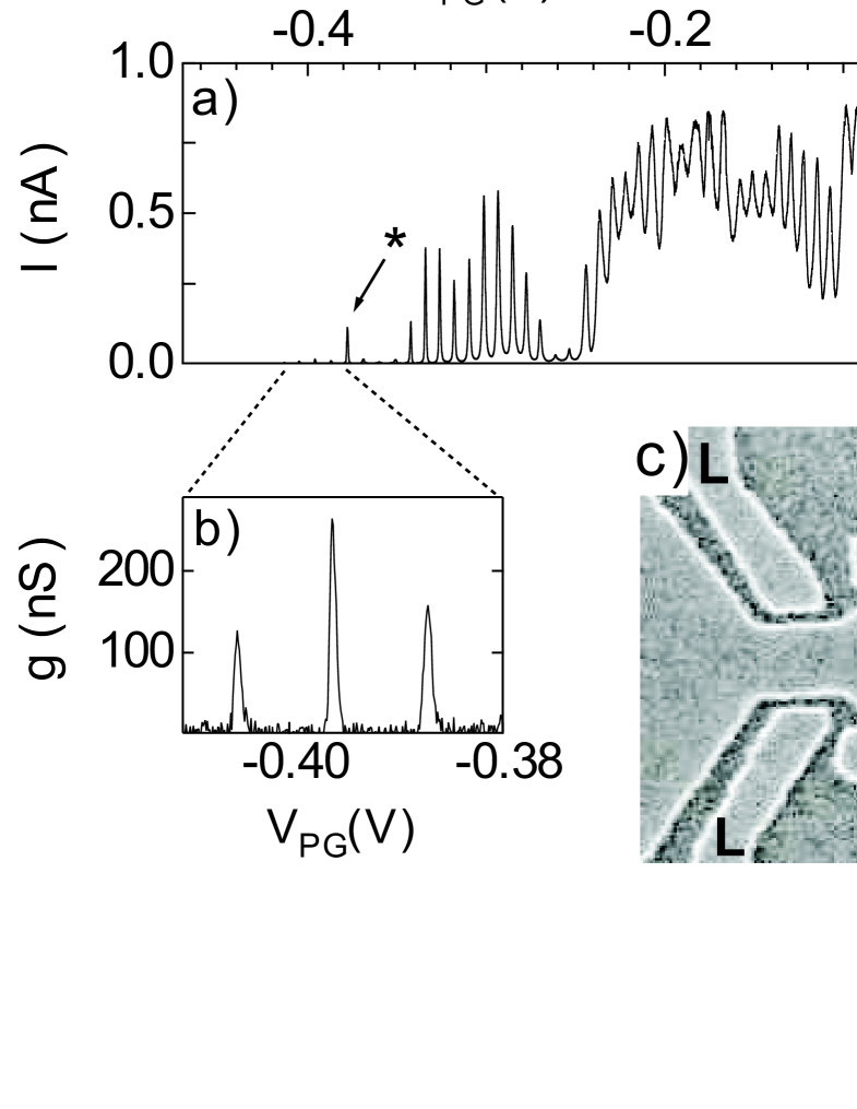
Figure 1(a) shows CB oscillations as the plunger gate is used to tune the dot occupancy. Similar oscillations are obtained by sweeping the other gates. Estimates of the respective gate capacitances can obtained from an analysis of the periodicity these oscillations (ignoring the discrete energy level structure of the dot). The capacitances obtained are aF, aF, aF and aF for the left QPC, right QPC, plunger gate and top gate respectively. The top gate is the dominant contribution at of the total gate capacitance of aF. We estimate that the dot contains at most electrons, based on the dot geometry, electron density and a nm depletion region at the dot walls, giving an energy level spacing eV. The CB oscillations in this device are quite sharp, and as shown in the close-up view of the last few resolvable CB peaks in Fig. 1(b), the conductance falls to zero for extended stretches between the CB peaks.
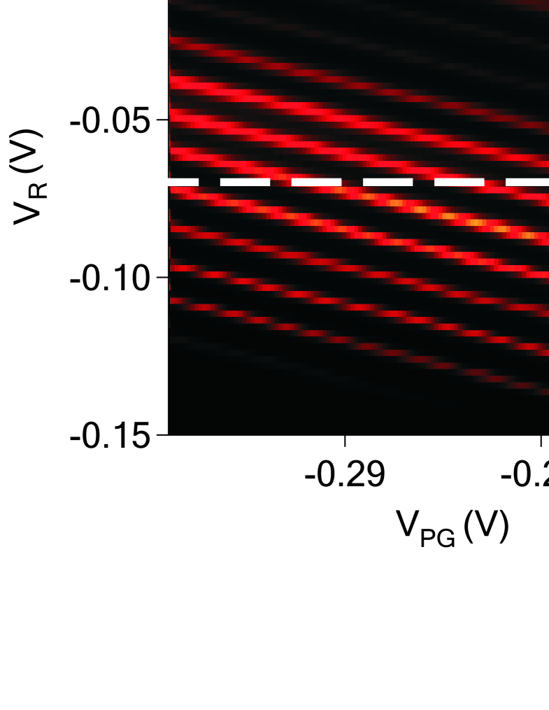
Figure 2 shows a color-map of the conductance versus right QPC gate bias and plunger gate bias . Bright regions mark the CB peaks, and the current is blockaded in the dark regions. The data in Fig. 1(a) corresponds to a slice along the horizontal white dashed line in Fig. 2. There is no evidence of charge trapping or random telegraph noise, which would produce discontinuous jumps in the bright lines in Fig. 2. In an ideal device free of crosstalk between the gates, the bright lines would be vertical; their relatively large slope indicates strong crosstalk between the right QPC and the plunger gate (similar data is obtained for the left QPC). This crosstalk is unavoidable due to the close proximity and similar capacitances of the QPC and plunger gate, but might be reduced with further optimization of the device design.
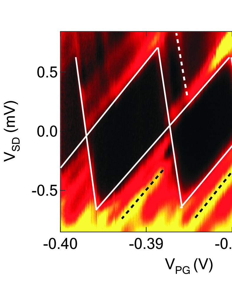
Bias spectroscopy measurements are shown in Fig. 3, where the conductance is plotted as a color-map versus the dc source-drain bias and . Dark regions indicate low , and form a sequence of ‘Coulomb diamonds’ (highlighted by the white solid lines) where current through the dot is blockaded. Kouwenhoven:2001rpp Again, there is no evidence of charge noise or random switching events in Fig. 3, demonstrating the stability of our device. The bright regions outside the Coulomb diamonds running parallel to the diamond edge (highlighted by white/black dashed lines) suggest transport via excited states in the dot. DeFrancheschi:2001prl The level spacing between the ground and excited states can be measured by the separation in between the excited state line and the diamond edge, with to eV. The level spacing is larger than the eV estimate obtained earlier, suggesting that the dot contains significantly fewer than electrons. This is likely due to lateral depletion caused by the shallow etch and fringing fields from the plunger and QPC gates. The charging energy can be directly extracted from an analysis of the Coulomb diamonds by subtracting from the half-diamond height, Hanson:2007rmp and ranges between and meV, varying slightly with dot occupancy. This charging energy corresponds to a total dot capacitance of aF, approximately consistent with the sum of the gate capacitances.
Further information was obtained from the temperature dependence of the CB peaks, in particular, from an analysis of their lineshape it is possible to differentiate whether the dot is in the classical or quantum transport regime. Beenakker:1991prb ; Folk:1996prl In the classical regime , the peak conductance is temperature independent and the peak full width at half maximum increases linearly with . In the quantum regime , goes as instead, with the linear relationship between and maintained. Beenakker:1991prb More rigorously:
| (1) |
in the quantum regime, where is the plunger gate ‘lever arm’ and is the plunger gate voltage relative to the center of the CB peak.
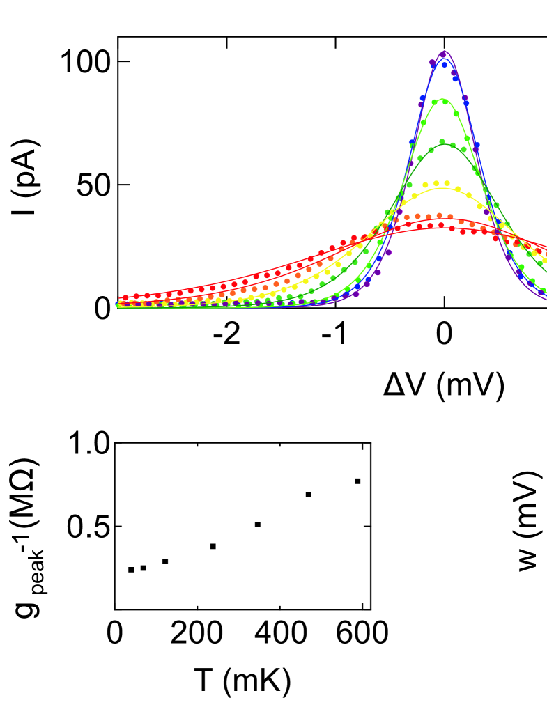
In Fig. 4(a), we show the temperature dependence for the CB peak centered at V for temperatures between and mK. The solid lines in Fig. 4(a) are fits of Eqn. 1 to the data with and as free parameters. In Fig. 4(b) we plot versus , with the linear trend confirming that our dot is in the quantum regime. In Fig. 4(c), we plot against , and from the gradient of the linear trend at higher we can extract the lever arm using the relationship . Folk:1996prl We obtain , which is consistent with , the average of the lever arms extracted from the left and the right diamonds of the same CB peak (Fig. 3). Finally, in Figs. 4(b/c) we observe saturation of both and as , providing an estimate of the minimum electron temperature in our device of mK.
In summary, we have fabricated quantum dots in AlGaAs/GaAs heterostructures without modulation doping. We use a heavily-doped cap layer, patterned into gates by electron-beam lithography and wet etching, to electrostatically control the electron population of the dot. Our device shows clear, stable CB oscillations in the quantum regime with transport via excited states in the dot also apparent. The improved noise performance afforded by removing the modulation doping makes this device architecture interesting for applications such as quantum information and ultra-sensitive electrometry where very stable quantum dots are extremely useful.
We thank M.A. Eriksson for helpful discussions. We acknowledge funding from the Australian Research Council (DP0772946). ARH acknowledges an ARC Professorial Fellowship.
References
- (1) :
- (2) U. Meirav, M.A. Kastner and S.J. Wind, Phys. Rev. Lett. 65, 771 (1990).
- (3) M.A. Kastner, Phys. Today 46(1), 24 (1993).
- (4) T. Fujisawa, T. Hayashi, Y. Hirayama, H.D. Cheong and Y. H. Jeong, Appl. Phys. Lett. 84, 2343 (2004).
- (5) D. Loss and D.P. DiVincenzo, Phys. Rev. A 57, 120 (1998).
- (6) R. Hanson, L.P. Kouwenhoven, J.R. Petta, S. Tarucha, L.M.K. Vandersypen, Rev. Mod. Phys. 79, 1217 (2007).
- (7) L.P. Kouwenhoven, C.M. Marcus, P.L. McEuen, S. Tarucha, R.M. Westervelt, and N.S. Wingreen, in Mesoscopic Electron Transport, edited by L.L. Sohn, L.P. Kouwenhoven and G. Schön, NATO ASI Ser. E, Vol. 345 (Kluwer, Dordrecht, 1997), pp. 105-214.
- (8) R. Dingle, H.L. Störmer, A.C. Gossard and W. Wiegmann, Appl. Phys. Lett. 33, 665 (1978).
- (9) C. Kurdak, C.J. Chen, D.C. Tsui, S. Parihar, and S.A. Lyon, Phys. Rev. B 56, 9813 (1997).
- (10) M. Pioro-Ladrière, J.H. Davies, A.R. Long, A.S. Sachrajda, L. Gaudreau, P. Zawadzki, J. Lapointe, J. Gupta, Z. Wasilewski and S. Studenikin, Phys. Rev. B 72, 115331 (2005).
- (11) C. Buizert, F.H.L. Koppens, M. Pioro-Ladrière, P. Tranitz, I.T. Vink, S. Tarucha, W. Wegscheider and L.M.K. Vandersypen, Phys. Rev. Lett. 101, 226603 (2008).
- (12) B.E. Kane, L.N. Pfeiffer and K.W. West, Appl. Phys. Lett. 67, 1262 (1995).
- (13) B.E. Kane, G.R. Facer, A.S. Dzurak, N.E. Lumpkin, R.G. Clark, L.N. Pfeiffer and K.W. West, Appl. Phys. Lett. 72, 3506 (1998).
- (14) O. Klochan, W.R. Clarke, R. Danneau, A.P. Micolich, L.H. Ho, A.R. Hamilton, K. Muraki and Y. Hirayama, Appl. Phys. Lett. 89, 092105 (2006).
- (15) U. Meirav, Single electron charging and periodic conductance oscillations in GaAs nanostructures, Ph.D. thesis, MIT (1990).
- (16) M. Heiblum, J. Vac. Sci. Technol. B 3, 820 (1985).
- (17) L.P. Kouwenhoven, D.G. Austing and S. Tarucha, Rep. Prog. Phys. 64, 701 (2001).
- (18) S. De Francheschi, S. Sasaki, J.M. Elzerman, W.G. van der Wiel, S. Tarucha and L.P. Kouwenhoven, Phys. Rev. Lett. 86, 878 (2001).
- (19) C.W.J. Beenakker, Phys. Rev. B 44, 1646 (1991).
- (20) J.A. Folk, S.R. Patel, S.F. Godijn, A.G. Huibers, S.M. Cronenwett, C.M. Marcus, K. Campman and A.C. Gossard, Phys. Rev. Lett. 76, 1699 (1996).