All Optical Integrated MOEMS Optical Coherence Tomography System
Abstract
Integrating all optical components of an optical coherence tomography (OCT) device into a single chip is a non-trivial and a challenging job. The design and development of such a lab-on-a chip will be possible only via Micro-Opto-Electro-Mechanical System (MOEMS) technology. The reproducible and integrated optical device fabrication would reduce cost and size many fold as compared to bulk or fiber optic OCT system. A miniaturized OCT of size less than 5mm2 area is designed, simulated and optimized. The successful fabrication of this device would help in point-of-contact devices as well as embedded biomedical sensor applications. Also, the design promises the possibility of fabrication of all optical components of OCT integrated into a single chip.
I Introduction
Significant advantage of integrated optical devices are its size, portability, mobility, multi-functional measurement capabilities, etc., over the bulk optical devices. Common methods adopted for the integration multiple optical components into a single chip is e-beam methods, pulse laser deposition, epitaxy methods, chemical vapor deposition or a cheaper photo-lithography. The developed micro-opto-electro-mechanical systems (MOEMS), once optimized can be used in industry, clinics, point-of-contact devices, mobile devices, etc. [1].
Optical coherence tomography (OCT) systems have been implemented so far using free-space or fiber optics components only. Although systems based on fiber optics allow for the compact, inexpensive and portable instrumentation, the final size and price of the devices are still not adequate for many applications. OCT systems composed of many optical components, such as: optical fibers, lenses beam splitters or directional coupler (DC), etc. These components are necessary to relay the optical signal through the OCT system. The combination of all these components makes OCT systems bulky, expensive and complex.
To solve above problem we will fabricate OCT system by using MOEMS fabrication technology. This technology has been proven that the low loss waveguide structure can be easily fabricated with either silicon on insulator waveguide technology or polymer (PMMA, SU8, S1813 etc) based waveguide. Before going for any waveguide fabrication process we need to simulate the system. In this article we simulate polymer based OCT system by using appropriate software codes.
II Theory
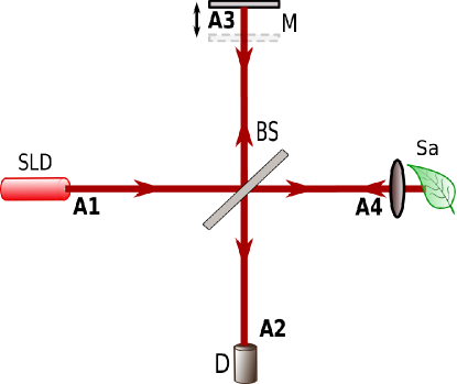
Figure 1, shows schematic of a free space OCT system. The heart of the OCT system is a Michelson Interferometer. The low coherence light beam entering at one arm (A1) of OCT is directed to reference (A3) and sample (A4) arms by beam splitter. The mirror in A3 is moved or scanned to induce a path difference mechanically or optically. The light scattered from the stratified media of the sample beam also return towards the detector. The back scattered light from A4 interfere with the back reflected light from the A3, when the path difference between them is within the coherence length of the light source [2, 3]. OCT measures the interference resulting from different axial locations within the tissue by moving the mirror at the reference arm which generates continuous interference signals along the depth. The depth-resolved sample information from each column of data is appended together and visualized as a 2-D cross-sectional image after signal processing.
We are proposing a polymer based MOEMS OCT system, where Michelson interferometer is fabricated using a waveguide bi-directional coupler. The moving mirror is replaced with an optical delay line generator. The delay line is integrated and replaced with the mirror component of the MI. The delay line which can generate temporal bunches of waves delayed in time is equivalent to the movement of a mirror.
II.1 Bi-directional coupler
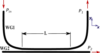
If two similar linear waveguides are parallel and sufficiently closely spaced over a length (coupling length) the energy is transferred from one to another due to the evanescent field between them. The fraction of the power coupled is determined by the overlap of the modes in the separate channels. In case of the synchronous co-directional coupler (both waveguide channels have same phase velocity, () all the energy can theoretically be transferred from one waveguide to another if is such that
| (1) |
with as the coupling constant and , Shown in Figure 2.
Generally, controls the ratio of power transferred between the waveguides. The value of depends on the percentage of overlap of the mode profiles within the waveguides. The coupling constant is generally defined as [Huns]
| (2) |
Here, - channel width, - separation between the channels, and are the propagation constants along the two transverse direction ( and axis) to propagation of wave (we suppose to direction of propagation of wave along axis) and is the exponential falloff along the direction of propagation of wave.
This principle is the basis for the operation of directional couplers, by adjusting the suitable coupling length , any desired portion of energy from a waveguide can be transferred into adjacent waveguide. In our case both waveguide channel have same phase velocity and we need to transfer same energy between both sample and reference arm so, we need to choose the coupling length such that 50% of light coupled from one waveguide to the adjacent one. Accordingly, the condition for 50:50 splitting ratio is [4],
| (3) |
II.2 Optical delay line
Optical delay line is another important functional component of OCT that provides optical delay at the reference arm to get interference signal with the back-scattered optical signals at sample arm and it also attends fast scanning speed and scan depth. Fiber optic delay lines are already been demonstrated [5]. Compact Silicon-Based Integrated Optic time delay line has been fabricated [6, 7] and demonstrated optical time delay. The silicon-on-insulator (SOI) technology is adopted with an incremental time delay of 12.3 ps. Guided- wave optical delay line provide the required precision and are more compact than optical fibers [8].
III Design and Working
The proposed lab-on a chip device of optical coherence tomography is exhibited in Figure 3. This design is divided into three sections: P1: Michelson interferometer with a 3dB coupler, P2: Y coupler for connecting the delay line with 3dB coupler and P3: Optical delay line.
Further a comparison of Figures 1 and 3, can be made to understand the arms of A1-A4 of MI with the proposed design.
The power distribution as shown in Figure 4, is discussed below. As we launched an optical power of from A1 arm of 3dB coupler, the light is divided into two equal parts to the arms A3 and A4. The optical power expected in the arms A3 and A4 is . A4 is sample arm and the arm A3 is connected to Y coupler. Further at P2 region the power is divided to to each YA1 and YA2 arms. Delay line consist of 20 C-channels separated at a pre-calculated distance. at YA1 arm, all C-channel is directly connected while in YA2 all C-channels (except 20th C-channel) is separated by a pre-calculated distances. Gap between lower YA2 arm and the C-channels are calculated for a leakage of 5% of optical power only.
1st C-channel decouples nearly 5% of optical power to the YA2 arm, corresponding to an optical power of . The remaining optical power is passed to 2nd and rest of the channels. The design ensure that all C-channels decouples a only 5% , and the remaining is passed on. While the power is splitted, each bunch of optical power also generates a path delay equivalent to 60m with each other. The path difference induces a temporal delay of about 0.6ps with next optical power. This pulse delay is typically required resolution in a OCT system. In other words the OCT system can resolve those two layers of samples whose optical distance is nearly 30m.
IV Results
We consider the fabrication of lab-on chip OCT system with
following parameters:
Design wavelength () = 1.55 m;
(SU 8); (air);
Channel width = 1 m; Radius of curvature of each C-channel = 6 m;
The estimated values of coupling length of each C-channel for constant power coupling of
in Table 1.
| C-channel # | C-channel # | ||||
|---|---|---|---|---|---|
| 1 | 5.00 | 4.0 m | 11 | 10.00 | 8.60 m |
| 2 | 5.26 | 4.2 m | 12 | 11.11 | 9.60 m |
| 3 | 5.56 | 4.5 m | 13 | 12.50 | 11.2 m |
| 4 | 5.88 | 4.8 m | 14 | 14.29 | 12.8 m |
| 5 | 6.25 | 5.2 m | 15 | 16.67 | 15.0 m |
| 6 | 6.67 | 5.7 m | 16 | 20.00 | 17.4 m |
| 7 | 7.14 | 6.2 m | 17 | 25.00 | 20.0 m |
| 8 | 7.69 | 6.5 m | 18 | 33.33 | 27.0 m |
| 9 | 8.33 | 7.0 m | 19 | 50.00 | 45.0 m |
| 10 | 9.09 | 7.7 m | 20 | 100.0 | Directly connected |
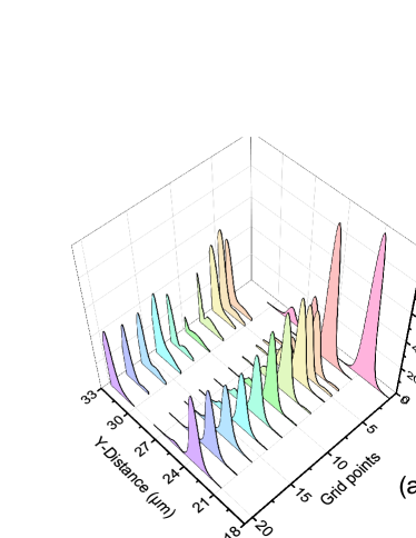
Simulation is performed using appropriate software code, where the complete structure as shown in Fig. 4 is used. All design parameters discussed above are incorporated. About 20 grid points as shown (in dashed gray lines) the figure are the places where measurements were made.
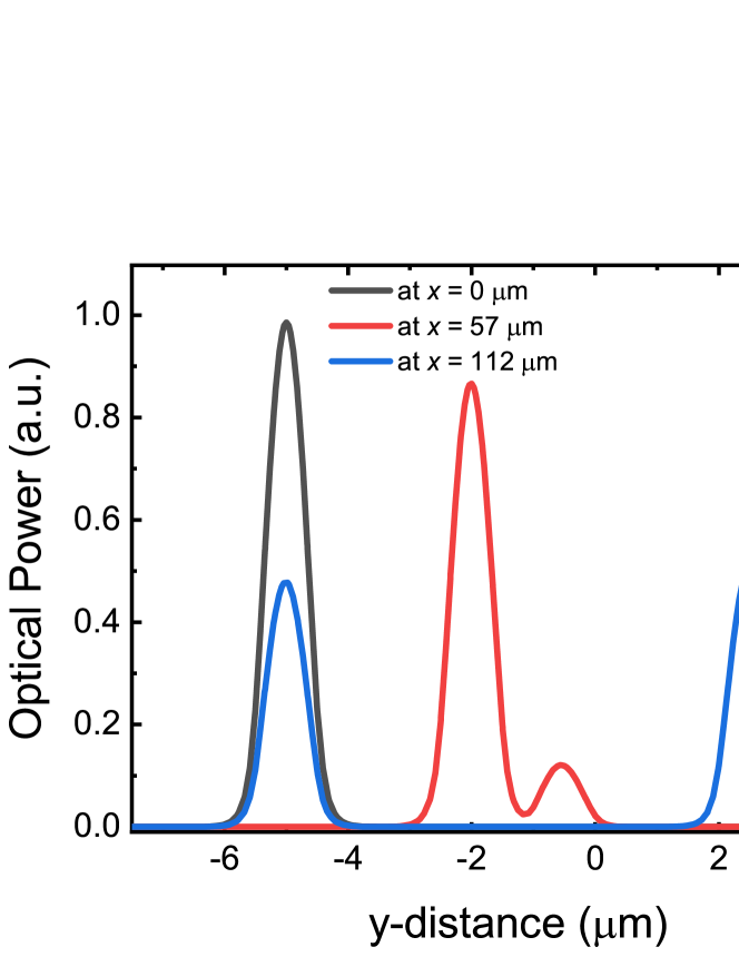
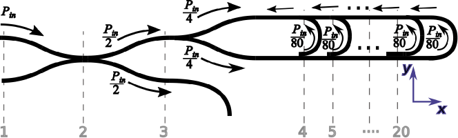
The Y-coupler as depicted as P1 in the design as simulated and studied first. The results are shown in Fig. 5. The measurements made at grid points 1, 2 and 3 are exhibited. The inset shows the power profile. The optical power coupled to the input port A2 is assumed as 100 % power. At grid point 3, the power is divided to 50:50 and act as 3dB coupler.
Simulation of the complete design as given in Fig. 4 is performed. The results obtained with optimized values are shown in Figure 6. The optical power profile values obtained at the grid point locations are plotted. The light is coupled at A2 port 18-19 m, region, YA1 is located at a distance of 23-24 m region while the C-channels ends at 25-26 m region. YA1 can be located at 31-32 m region.
Figure 6a, clearly demonstrates the capability of all the components P1, P2 and P3. The expected 50:50 ratio may be noted at grid point 3. The power is further makes round trips via YA1 to YA2 as well as through YA2 to YA1. Both outputs reaches the directional coupler and A2 arm.
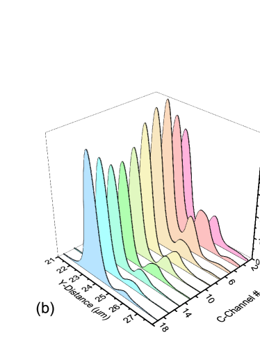
The magnified and enhanced view of YA2-C-channel region is depicted in Fig 6b. The results shows light coupling between these channels. However, expected values of 5% optical power from each channel could not be found. A exponential decay of power reduction happens at channels 10 and beyond. Overall we could see that required delay is generated, but with slight change in power ratio. The change power ratio might change the visibility of the images only.
V Conclusions
We proposed a design of all optical optical coherence tomography system using SU-8 polymer. The simulated results shows the definite possibility of miniaturized OCT. The lab-on-a-chip design dimensions are : length = 1.4mm and width = 50 m approx. The area of the chip after embedding the detector and light source would be less than 2mm2. This promises the possibility of fabrication of all optical OCT for point of contact devices as well as for embedded OCT chip a reality.
Acknowledgments
ASB and JTA acknowledge the financial support received from SERB, New Delhi GoI, under the project number CRG/2018/003871.
References
References
- [1] Li, B., Huang, L., Qiu, Z. (2022), MOEMS-Enabled Miniaturized Biomedical Sensing and Imaging System Springer, Cham.
- [2] Huang, D., Swanson, E. A., Lin, C. P., Schuman, J. S., Stinson, W. G., Chang, W., Hee, M. R., Flotte, T., Gregory, K., Puliafito, C. A. and Fujimoto, J. G. (1991), Optical Coherence Tomography Science. 254, 1178-1181.
- [3] Drexler W and Fujimoto J G 2015 Optical Coherence Tomography: Technology and Applications ed Springer (Switzerland: Springer International Publishing).
- [4] T. Tamir, Topics in Applied Physics Integrated Optics 1982 second edition pp. 124-125.
- [5] Choi, E., Jihoon, N., Seon, R. Y., Gopinath, M. and Byeong, H. L. (2005) All-fiber variable optical delay line for applications in optical coherence tomography: feasibility study for a novel delay line Optical Express 13(4), 1334.
- [6] Yegnanarayanan, S., Trinh, P. D., Coppinger, F. and Jalali, B. (1997), Compact silicon based Integrated Optical Time Delays, IEEE Photonics technology letters 9(5), 634-635.
- [7] O. P. Chaudhary, S. Chouksey, P. K. Sen, P. Sen, J. Solanki and J T Andrews (2014) MOEMS Optical delay line for optical coherence tomography J. Phys.: CS. 534 012066.
- [8] Alameh, K., Sampson, D., Wang, Z., Zheng, R. and Poh., C. K., eds (2005), Broadband Static Micro-Delay lines generation for OCT, IFIP, Conference Proceeding of VLSI-SoC.