Atomic layer etching of InGaAs using sequential exposures of atomic hydrogen and oxygen gas
Abstract
The high frequency performance and yield of III-V semiconductor devices such as InP HEMTs is negatively impacted by subsurface etch damage and non-uniform etch depth over the wafer. Atomic layer etching (ALE) has the potential to overcome this challenge because of its ability to etch with Angstrom-scale precision, low damage, and intrinsic wafer-scale uniformity. Here, we report an ALE process for InGaAs based on sequential atomic hydrogen and oxygen gas exposures. An etch rate of 0.095 Å/cycle was observed at 350 \degreecelsius using ex-situ spectroscopic ellipsometry. The sample remains atomically smooth after 200 cycles of ALE. This process could be employed as a gate recess etch step in InP HEMT fabrication to improve microwave performance and yield.
I Introduction
III-V compound semiconductors such as InGaAs and InAlAs are of high importance for both fundamental science and applications. In particular, high electron mobility transistors (HEMTs) based on InGaAs/InAlAs quantum wells are widely used for remote sensing [1], radio astronomy [2, 3], communications [4, 5], and increasingly quantum computing due to their outstanding noise performance [6, 7, 8]. A critical step in HEMT fabrication is the gate recess etch in which the cap (consisting of highly doped InGaAs) and a portion of the barrier (undoped InAlAs) are etched to place the gate electrode as close as possible to the conducting channel while maintaining a low leakage current ( A/mm) [9, 10]. The desired etch depth precision is around a nanometer over the wafer, which is challenging to achieve with typical wet or dry etching due to local variations in etch rate. Etching non-uniformities degrade yield, and etch-induced damage limits the degree of scaling that can be achieved, which in turn sets high frequency performance limits [11]. Etch damage also leads to the formation of electrical traps at the gate-barrier Schottky junction which causes gain instabilities [12, 13, 14].
Atomic layer etching (ALE) is an emerging nanofabrication technique that consists of a set of sequential and self-limiting half-steps that together produce etching [15]. ALE is analogous to atomic layer deposition (ALD) except that the half-steps produce etching rather than deposition. An ALE process generally consists of a modification step followed by a selective removal of the modified surface layer. The removal of this modified layer defines whether the ALE is thermal (isotropic) or directional (anisotropic). Directional ALE was demonstrated first, and it exploits the difference in surface binding energy to sputter only the modified layer with ions or neutral atoms [16]. In 2015, thermal ALE based on ligand-exchange reactions was first reported [17]. Since then, several other approaches for thermal ALE have been reported.
Thermal ALE of InGaAs has previously been demonstrated using vapor HF to form fluoride compounds and ligand-exchange for volatilization using dimethylaluminum chloride (DMAC) [18]. This process had an etch per cycle (EPC) of around 0.1 Å/cycle and was used to fabricate an InGaAs FinFET with record performance [19]. Directional ALE of InGaAs has also been explored using chlorine radicals as the modification step and low energy Ar ions to sputter the modified surface layer [20]. This process was reported to achieve an EPC of 1.1 Å/Cycle and lower surface roughness than was achieved with reactive ion etching. Despite these advances, processes which preserve the stoichiometry of the ternary alloy while inducing as little surface damage as possible remain of interest.
Here, we report an ALE process for InGaAs based on sequential exposures of hydrogen radicals and oxygen gas. The process exhibits an etch rate of around 0.1 Å/cycle. Both half cycles are observed to be self-limiting. The process preserves the atomic-scale smoothness of the epitaxial wafer over 200 cycles. XPS analysis indicates that In compounds are preferentially etched over Ga compounds. The process has potential for integration into InP HEMT fabrication to enable improved yield and high-frequency microwave performance.
II Methods
The samples consisted of an epitaxial stack of InGaAs and InAlAs films grown on an InP substrate by molecular beam epitaxy. The top film was a 200 nm thick lattice-matched n-In0.53Ga0.47As layer with carrier concentration of cm-3, below which was a 200 nm lattice matched In0.52Al0.48As buffer. The films were grown on 2 inch InP wafers and diced into mm chips. Prior to use, the chips were spin cleaned with acetone followed by isopropyl alchohol at 4000 rpm.
ALE experiments were carried out in an Oxford Instruments FlexAL II atomic layer deposition tool. Hydrogen plasma was generated through an inductively coupled plasma (ICP) source. To limit ion damage to the chip, a pseudo-remote plasma was achieved by encasing the chip in a roof structure to eliminate direct line of sight between the chip and the ICP plasma source. The roof structure was a mm sapphire chip supported by two mm sapphire chips, forming a channel in which the chip sits. This structure allows gas reactants to diffuse to the chip while minimizing direct ion impingement.
Thickness changes due to etching were measured by ex-situ ellipsometry using a J.A. Woolam M-2000 spectroscopic ellipsometer. Measurements were taken in the center of the chips in a line perpendicular to the channel of the roof structure with points spaced 1 mm apart to avoid edge effects from the roof structure. Chips were placed in the same position and orientation before and after etching. Ellipsometry data was taken between 370-1000 nm at angles of 60, 65, and 70 degrees. The data was fit using J.A. Woollam CompleteEASE software with a model consisting of InGaAs oxide, In0.53Ga0.47As, In0.52Al0.48As, and InP.
Before ALE, preconditioning of the chamber was performed to ensure a consistent initial chamber condition. The vacuum chamber chuck was heated to the process temperature of \degreecelsius to allow it to thermalize while the rest of the preconditioning was carried out. Next, 6 minutes of Ar/O2/SF6 plasma (120 sccm Ar, 40 sccm SF6, 40 sccm, O2) was performed, followed by 300 cycles of alumina ALD ( nm). Alumina was chosen as it is does not react with the oxygen gas and hydrogen plasma used during ALE. Finally, 50 cycles of the ALE recipe was performed, after which the chip was loaded into the reactor.
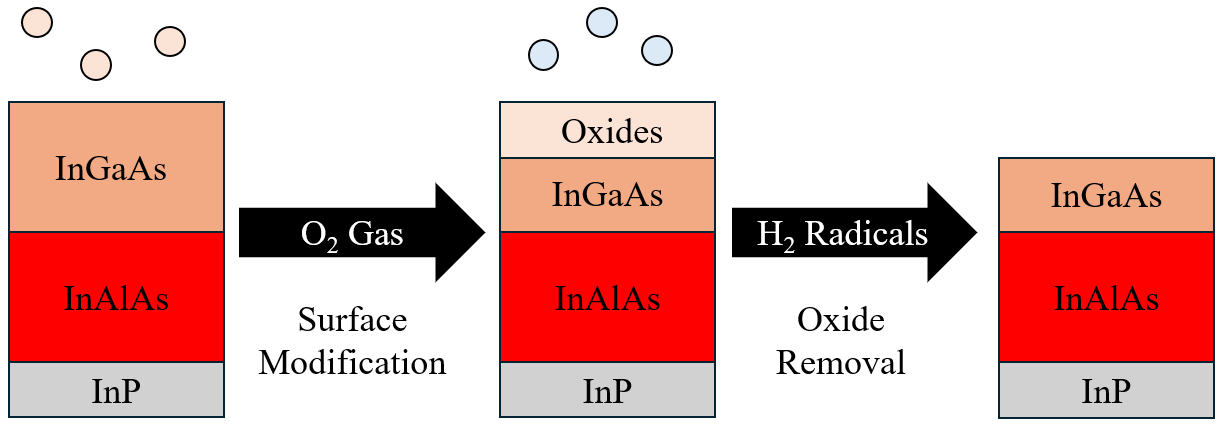
The chip was then allowed to heat to \degreecelsius for 4 minutes while Ar was flowed at 100 sccm, with a chamber pressure of 100 mTorr. The ALE process was then carried out as shown in Figure 1. First, 50 sccm of H2 was flowed for 10 seconds, reaching a stable chamber pressure of 100 mTorr after which a plasma was struck at 100 W and held for 2 minutes. The chamber was then purged for 2 seconds with 200 sccm of Ar and then pumped down for 10 seconds. This initial 2 min H2 exposure was used to remove the oxide formed when the sample is removed from the chamber to perform ex-situ ellipsometry.
The main ALE cycle was then carried out as follows. The oxidation half step was performed by flowing 100 sccm of O2 for 45 seconds reaching a chamber pressure of 225 mTorr. The chamber was then purged by flowing 300 sccm of Ar for 3 seconds and then pumping down for 10 seconds. After this, the hydrogen plasma half cycle was carried out by first flowing 50 sccm of H2 for 10 seconds at 100 mTorr and then striking and holding a 100 W plasma for 1 minute. The chamber was then purged with Ar and then pumped down for 10 seconds before restarting the ALE cycle. After processing the chamber was pumped down for 1 minute before the chip was unloaded to the load-lock. The chip was then held in dry nitrogen atmosphere in the load-lock for 5 minutes to cool.
The saturation curves were acquired at constant chamber temperature, pressure, and ICP plasma power, only varying the times of the oxygen gas and hydrogen radical exposures in their respective saturation curves while holding the other constant. The same purging and pumping was used for all processes. The saturation curves were obtained using a single sample. After the chips were preconditioned, the initial film thicknesses were determined via ellipsometry. The chips then underwent 100 cycles of ALE for a given half cycle exposure time before being measured again by ellipsometry. This process was repeated to generate the saturation curve.
Surface roughness measurements were taken using a Bruker Dimension Icon atomic force microscope (AFM). PeakForce tapping mode was used with a ScanAsyst-Air AFM probe. A nm square region was scanned by segmenting the region into 1024 lines each of which contains 1024 points where data was collected. The raw height maps were processed using the NanoScope Analysis software from Bruker. This raw data was processed using a 2D flatten and low pass filter to remove tilt angle and scan artifacts. The power spectral density (PSD) was then calculated using Nanoscopes’s 2D isotropic PSD feature.
Surface characterization was performed via ex-situ X-ray photoelectron spectroscopy (XPS) using a Kratos Axis Ultra XPS with a monochromatic Al K source. To perform depth profiling, an Ar ion beam was used to mill the sample in 30 s cycles, and data were collected for 8 subsurface points. The XPS data was processed using CASA-XPS from Casa Software Ltd. The backgrounds were taken to be Shirley and the line-shape of the In, Ga, and As peaks were taken to be a mix of Gaussian and Lorentzian. The exact ratio of the line-shape was determined by minimizing the residual of the individual peaks in the bulk where no oxide was present. To compare atomic percentages, the Scofield relative sensitivity factors were used, which recovered the expected In:Ga ratio of 1.13 in the bulk.
III Results
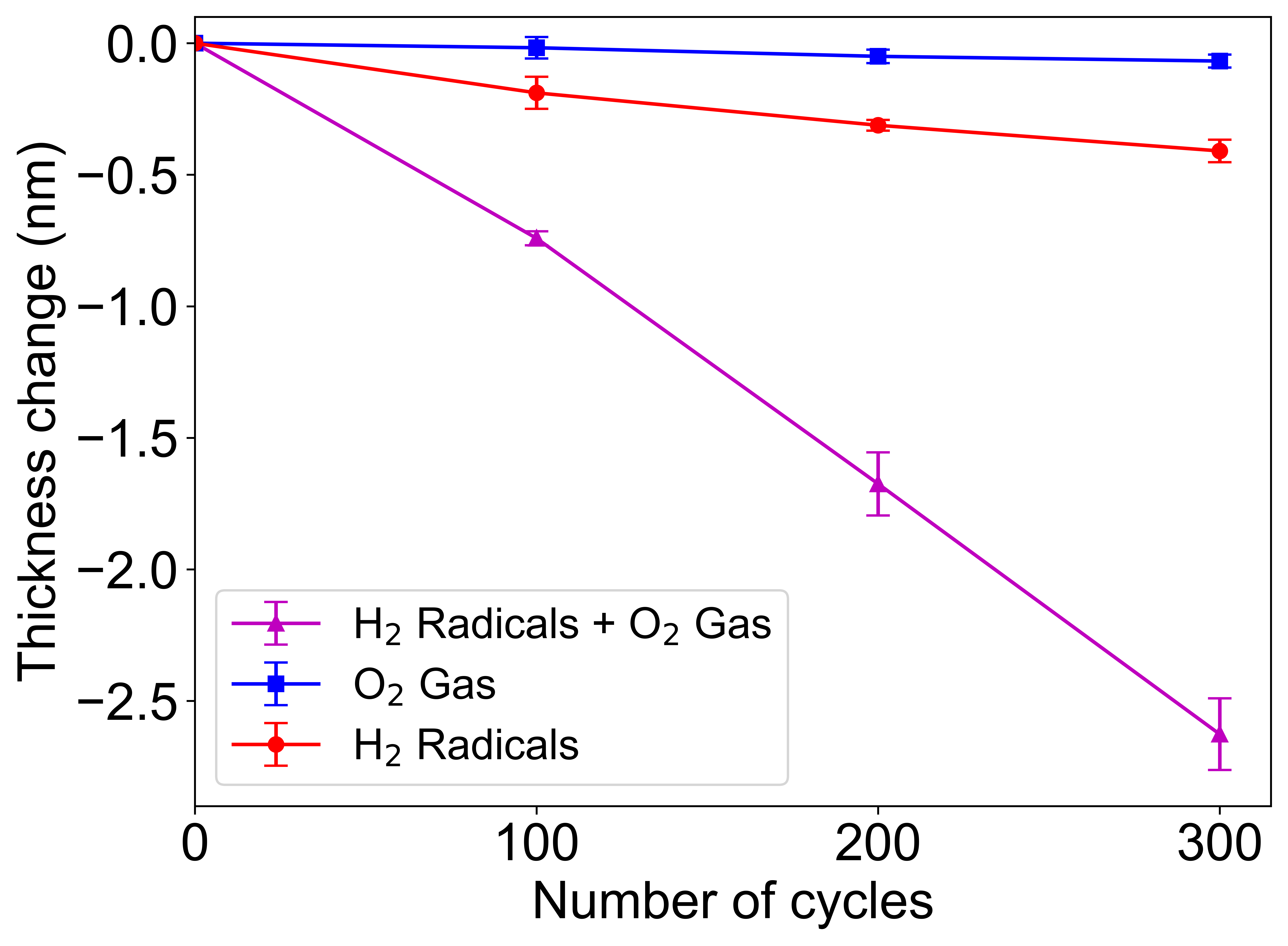
We begin by comparing the change in sample thickness with respect to cycle number for oxygen gas, hydrogen radicals, and both half steps as shown in Figure 2. We observe that the exposure of InGaAs to just oxygen gas has a negligible etch rate of 0.002 Å/cycle. Exposure to only hydrogen radicals has a slightly higher EPC of 0.014 Å/cycle. This EPC value can likely be attributed to the use of ex situ ellipsometry to measure the sample thickness, meaning that the sample is exposed to ambient air for some time prior to the measurement. As a result, some thickness of native oxide is formed which is then etched by the next hydrogen radical exposure. This etched thickness is included in the EPC for hydrogen radicals. It is expected that the EPC excluding this effect is negligible.
Combining the two half cycles, we observe an EPC of 0.095 Å/cycle. The EPC was obtained by dividing the total thickness change after 300 cycles by the number of cycles. We note that to minimize process times, the sample was reused to obtain the thickness change after 100, 200, and 300 cycles, rather than using a new sample for each data point. This EPC is similar to the previously reported EPC of thermal ALE of InGaAs using HF and DMAC for which an etch rate of 0.10 Å/cycle at 250 \degreecelsius was reported [18].
The chemistry for this etching has been extensively studied in the context of ultrahigh vacuum surface cleaning of III-V semiconductors using hydrogen radicals. [21, 22] The generally accepted reactions are:
| (1) | |||
| (2) | |||
| (3) |
where the uparrow indicates volatile species under vacuum. These reactions are all known to proceed with volatile products at temperatures above 200 \degreecelsius[21, 22, 23, 24].
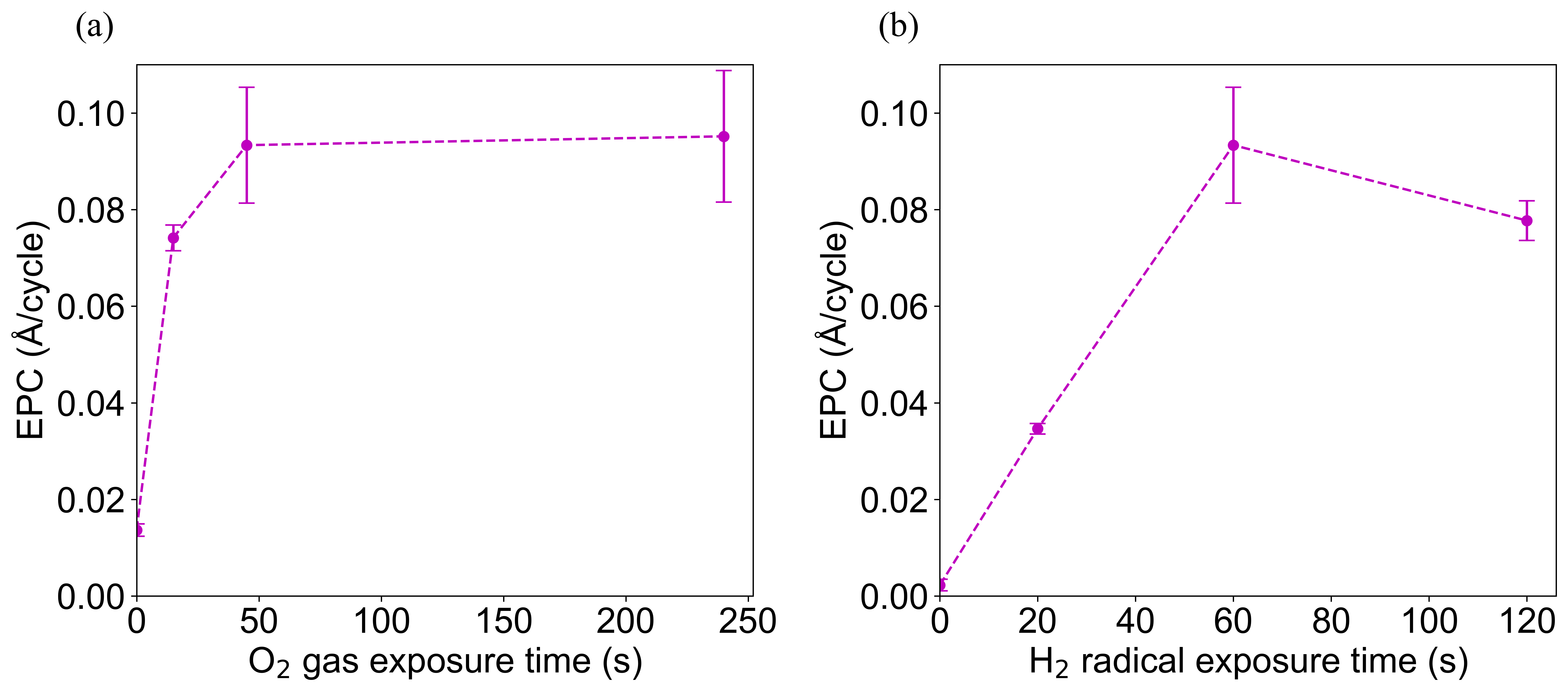
To gain further insight into the process, we measured the saturation curves for both the hydrogen radical and oxygen gas half cycles. Figure 3 shows the O2 gas saturation curve. It is observed that the EPC increases with increasing O2 gas exposure time until an exposure of 45 seconds is reached, after which the EPC plateaus. It is concluded that the oxygen half cycle has reached saturation at a 45 second per cycle exposure. Next, Figure 3 shows the H2 plasma saturation curve. This plot likewise shows that increasing the hydrogen plasma exposure time increases the EPC until 60 seconds after which it appears that the etch rate decreases slightly, although the EPC plateaus within uncertainty. This mild decrease could be due to H ion damage as the ion flux is non-negligible for sufficiently long exposures, despite the use of the roof structure. However, considering prior studies of hydrogen radicals with native oxides of InGaAs, saturation of the hydrogen radical step is expected. We take the saturated ALE conditions to be 45 seconds of O2 and 60 seconds of H2 radicals for a process temperature of 350 \degreecelsius.
The temperature dependence of the EPC was surveyed by running 200 cycles with saturated parameters at \degreecelsius, \degreecelsius, and \degreecelsius. The EPC is found to increase by around 45% at a temperature of 400 \degreecelsius, likely due to the increase in solid-state diffusivity of the oxygen gas molecules. The etch rate appeared negligible at 300 \degreecelsius using the saturated process conditions at 350 \degreecelsius. A prior study has shown InGaAs oxides may be removed as low as 192 \degreecelsius with an exposure time of 10 minutes [25]. Therefore, we expect that etching could be possible at lower temperatures with longer cycles times or higher hydrogen radical density. This topic will be investigated in a future study.
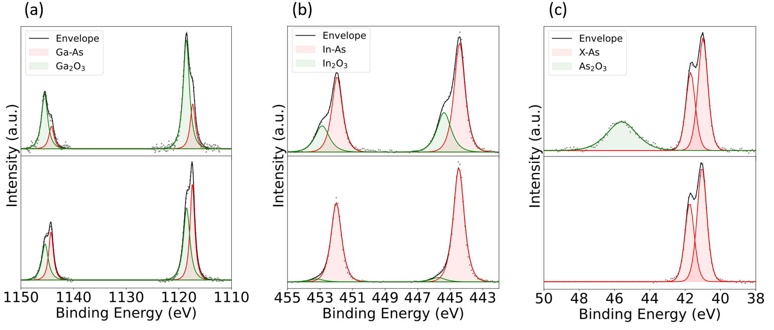
Next, we analyze the surface chemical composition of the InGaAs samples before and after ALE using ex-situ XPS. Figure 4 shows the core level spectra for In3d, As3d, and Ga2p before and after 200 cycles of ALE. It is observed that the In and Ga core level spectra have 2 doublet peaks. There are two peaks due to the spin orbital splitting of these levels, 3d5/2 and 3d3/2 for In and 2p1/2, 2p3/2 for Ga, and they are doublets due to the fact these metals have two distinct chemical bonding environments: one metallic and one involving bonding with oxygen. The higher energy peak in the doublet corresponds to the oxides. Whereas, the doublet in the As spectra is due to spin orbital splitting (3d5/2 and 3d3/2) and the broad peak higher in energy corresponds to its oxidation states.
Qualitatively, it is seen that there are relatively fewer surface oxides after ALE despite the samples being exposed to ambient air prior to XPS. The proportion of indium oxide on the surface has also decreased relative to gallium oxide, and there is no detectable As oxide on the surface after ALE. It is difficult to determine if this difference is simply from the oxidation of the sample after leaving the etching chamber or if the process conditions result in preferential etching which could potentially terminate etching over a large cycle number. This topic will be investigated in a future study.
| In (%) | As (%) | Ga (%) | O (%) | C (%) | |
|---|---|---|---|---|---|
| Original | 11.43 0.07 | 19.16 0.27 | 3.45 0.06 | 35.26 1.34 | 30.70 2.41 |
| ALE | 20.57 0.08 | 31.56 0.35 | 12.21 0.22 | 23.26 2.85 | 12.41 1.22 |
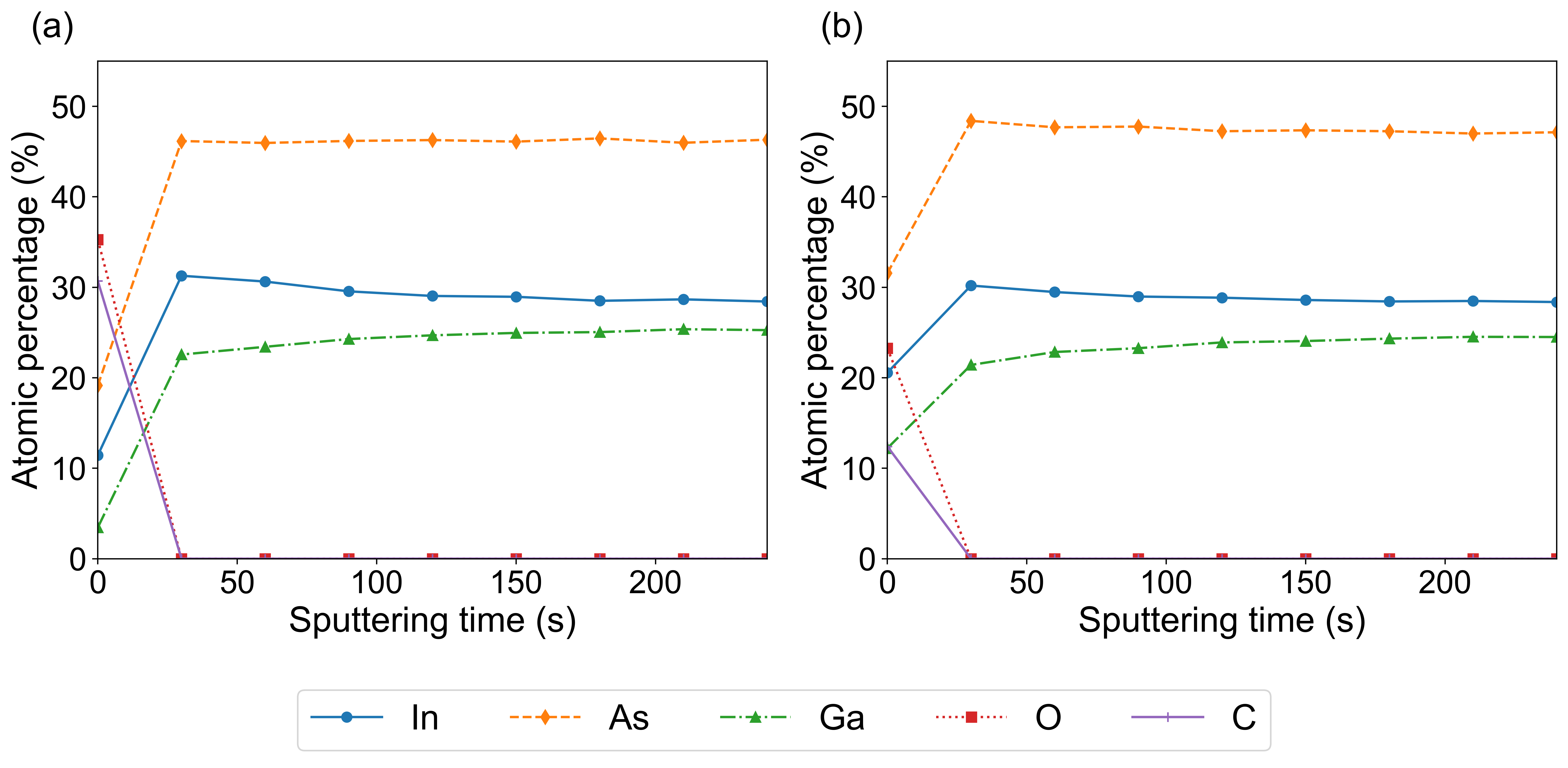
To assess the degree to which the processing is confined to the surface region, XPS depth profiling was performed. The atomic concentration of O, C, In, Ga, and As with respect to milling time for both the original sample and a sample etched with 200 cycles of ALE are shown in Figure 5. The bulk atomic composition after ALE was observed to be within 97% of the values of the original sample. Furthermore, the bulk ratio of In:Ga was around 1.13. The surface composition of both the original and the ALE sample is shown in Table 1. Here, it is observed that after ALE the surface atomic concentration of oxygen decreases by 34.0%. It was also observed that the ratio of In:Ga was halved after ALE. However, the In:Ga ratio after ALE, 1.7, is still above the bulk ratio. It should be noted that the original sample surface was In rich. It is unclear if this apparent decrease in In from ALE will continue past the bulk stoichiometry for higher cycle number.
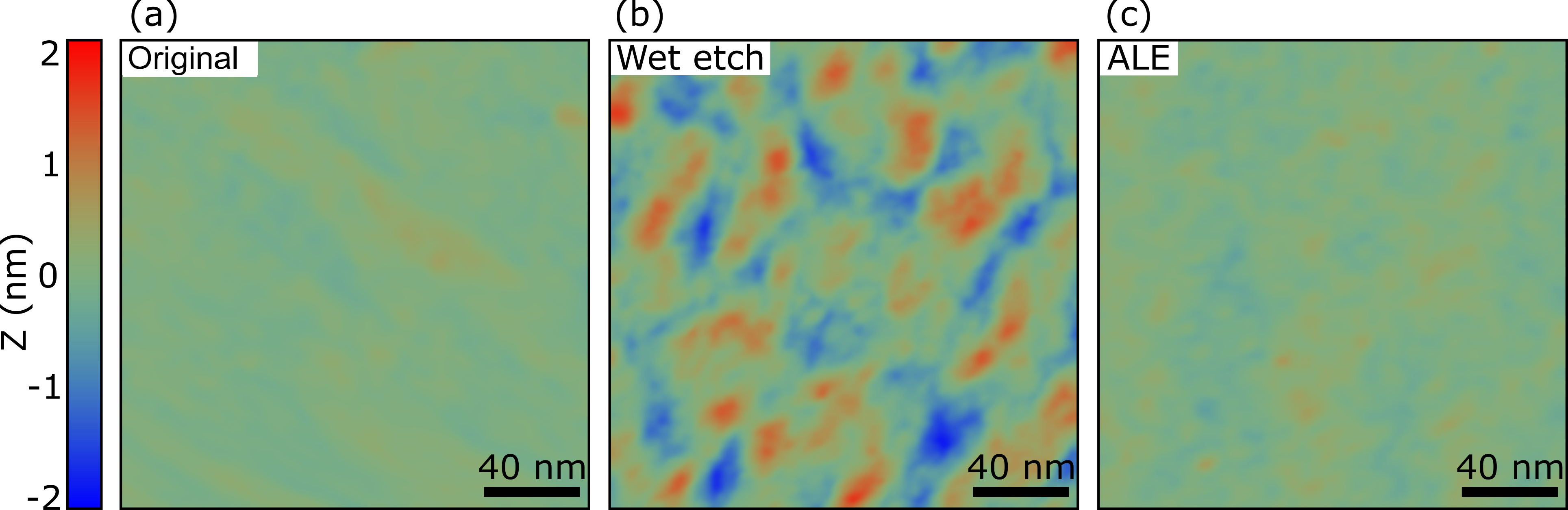
We used AFM to characterize the surface roughness of a original InGaAs sample with its native oxide, a sample subjected to 200 cycles of ALE (etch depth of 2 nm), and a sample etched for 5 s (etch depth of nm) with a citric acid/H2O2 wet etch. Figure 6 shows a height map of the surface of these samples. The original sample (Figure 6) has a nm, as expected for an epitaxially grown film. The wet etched sample (Figure 6) is visibly rougher with an nm. The ALE sample (Figure 6) has an which is indistinguishable from that of the MBE grown sample.
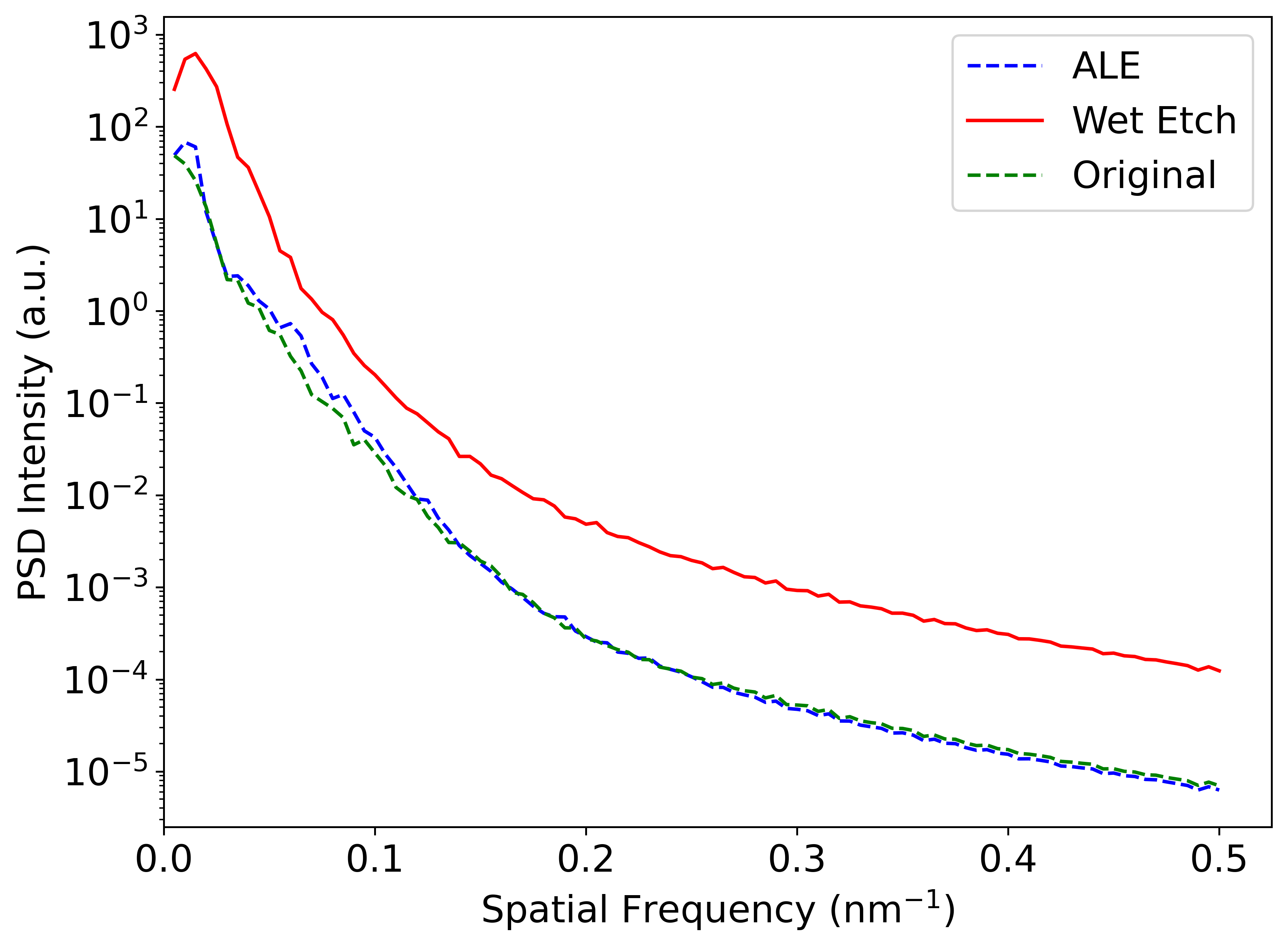
Power spectral density (PSD) is another way to quantify surface roughness over characteristic length scales as quantified by the spatial frequency. The PSD of the AFM scans is shown in Figure 7. It is observed that the wet-etched sample has a higher PSD over all spatial frequencies compared to the original sample. On the other hand, the ALE sample exhibits a PSD which nearly coincides with that of the original sample. This result further confirms that 200 cycles of ALE does not increase the surface roughness.
 \phantomsubcaption\phantomsubcaption\phantomsubcaption
IV Discussion
Our ALE process has potential applications for III-V compound semiconductor devices by enabling precise etch control on the Angstrom scale with wafer-scale uniformity. Unlike continuous wet or dry etching processes which are subject to local variations in etch rate over a wafer, ALE is inherently scalable to arbitrary wafer sizes owing to the use of self-limiting surface chemical reactions. Our process may find application as gate recess etching for InP HEMTs where sub-nanometer precision in the etch depth over a 3” or larger InP wafer is desired for optimal yield. The low surface damage of ALE compared to traditional wet or dry etches may facilitate more aggressive device scaling, leading to improved high frequency performance. A lower electrical trap density on the ALE-treated surface is also expected, which could lead to improved gain stability.
Future work should employ a downstream plasma or thermal source of hydrogen radicals to eliminate ion damage while also providing a higher radical density. Additional study is needed to assess whether the process also etches the InAlAs barrier film. Finally, surface passivation schemes for the exposed InAlAs need to be developed. ALE offers the possibility for in-situ passivation of this surface in the clean environment of high vacuum, potentially via formation of a crystalline oxide followed by atomic layer deposition, [26] or other schemes.
V Conclusion
We have reported an ALE process for InGaAs consisting of sequential hydrogen radical and oxygen gas exposures. We observe an etch rate of 0.095 Å/cycle and that both half-cycles exhibit self-limiting behavior. The process preserves the atomic-scale smoothness of the original epitaxial wafer after 200 cycles of ALE. The process has potential for applications in fabrication of InP HEMTs with improved high frequency performance and gain stability.
VI Acknowledgements
The authors thank Andrew Carter for useful discussions. This prototype (or technology) was partially supported by the Microelectronics Commons Program, a DoD initiative, under award number N00164-23-9-G056, and the Rothenberg Innovation Initiative (RI2) at the California Institute of Technology. This material is based upon work supported by the National Science Foundation under Grant No. 191122. We gratefully acknowledge the critical support and infrastructure provided for this work by The Kavli Nanoscience Institute at the California Institute of Technology. Research was in part carried out at the Molecular Materials Research Center in the Beckman Institute of the California Institute of Technology. This work was performed, in part, at the Center for Integrated Nanotechnologies, an Office of Science User Facility operated for the U.S. Department of Energy (DOE) Office of Science. Sandia National Laboratories is a multimission laboratory managed and operated by National Technology & Engineering Solutions of Sandia, LLC, a wholly owned subsidiary of Honeywell International, Inc., for the U.S. DOE’s National Nuclear Security Administration under contract DE-NA-0003525. The views expressed in the article do not necessarily represent the views of the U.S. DOE or the United States Government
VII Data availability statement
The data that support the findings of this study are available from the corresponding author upon reasonable request.
VIII Conflict of interest
The authors have no conflicts to disclose.
References
- [1] William R. Deal and Goutam Chattopadhyay. InP HEMT integrated circuits for Submillimeter Wave radiometers in earth remote sensing. In 2012 IEEE/MTT-S International Microwave Symposium Digest, pages 1–3. IEEE, Montreal, QC, Canada, June 2012. ISBN 978-1-4673-1088-8 978-1-4673-1085-7 978-1-4673-1087-1 978-1-4673-1086-4. URL http://ieeexplore.ieee.org/document/6258434/.
- [2] Marian W. Pospieszalski. Extremely low-noise cryogenic amplifiers for radio astronomy: past, present and future. In 2018 22nd International Microwave and Radar Conference (MIKON), pages 1–6. IEEE, May 2018.
- [3] Chau-Ching Chiong, Yunshan Wang, Kai-Chun Chang, and Huei Wang. Low-Noise Amplifier for Next-Generation Radio Astronomy Telescopes: Review of the State-of-the-Art Cryogenic LNAs in the Most Challenging Applications. IEEE Microwave Magazine, 23(1):31–47, January 2022. ISSN 1557-9581. Conference Name: IEEE Microwave Magazine.
- [4] H. Hamada, T. Tsutsumi, H. Sugiyama, H. Matsuzaki, H.-J. Song, G. Itami, T. Fujimura, I. Abdo, K. Okada, and H. Nosaka. Millimeter-wave InP Device Technologies for Ultra-high Speed Wireless Communications toward Beyond 5G. In 2019 IEEE International Electron Devices Meeting (IEDM), pages 9.2.1–9.2.4, December 2019. URL https://ieeexplore.ieee.org/document/8993540/. ISSN: 2156-017X.
- [5] Wan-Soo Park, Hyeon-Bhin Jo, Hyo-Jin Kim, Su-Min Choi, Ji-Hoon Yoo, Hyeon-Seok Jeong, Sethu George, Ji-Min Baek, In-Geun Lee, Tae-Woo Kim, Sang-Kuk Kim, Jacob Yun, Ted Kim, Takuya Tsutsumi, Hiroki Sugiyama, Hideaki Matsuzaki, Jae-Hak Lee, and Dae-Hyun Kim. Sub-50 nm Terahertz In Ga As Quantum-Well High-Electron-Mobility Transistors for 6G Applications. IEEE Transactions on Electron Devices, 70(4):2081–2089, April 2023. ISSN 0018-9383, 1557-9646. URL https://ieeexplore.ieee.org/document/10014673/.
- [6] Joseph C. Bardin. Cryogenic Low-Noise Amplifiers: Noise Performance and Power Dissipation. IEEE Solid-State Circuits Magazine, 13(2):22–35, 2021. ISSN 1943-0590. Conference Name: IEEE Solid-State Circuits Magazine.
- [7] Joseph C. Bardin, Daniel H. Slichter, and David J. Reilly. Microwaves in Quantum Computing. IEEE Journal of Microwaves, 1(1):403–427, January 2021. ISSN 2692-8388. Conference Name: IEEE Journal of Microwaves.
- [8] Junjie Li, Johan Bergsten, Arsalan Pourkabirian, and Jan Grahn. Investigation of Noise Properties in the InP HEMT for LNAs in Qubit Amplification: Effects From Channel Indium Content. IEEE Journal of the Electron Devices Society, 12:243–248, 2024. ISSN 2168-6734. URL https://ieeexplore.ieee.org/document/10454583/?arnumber=10454583. Conference Name: IEEE Journal of the Electron Devices Society.
- [9] Tamara Saranovac, Anna Hambitzer, Diego C. Ruiz, Olivier Ostinelli, and C. R. Bolognesi. Pt Gate Sink-In Process Details Impact on InP HEMT DC and RF Performance. IEEE Transactions on Semiconductor Manufacturing, 30(4):462–467, November 2017. ISSN 1558-2345. Conference Name: IEEE Transactions on Semiconductor Manufacturing.
- [10] Junjie Li, Arsalan Pourkabirian, Johan Bergsten, Niklas Wadefalk, and Jan Grahn. Influence of Spacer Thickness on the Noise Performance in InP HEMTs for Cryogenic LNAs. IEEE Electron Device Letters, 43(7):1029–1032, July 2022. ISSN 1558-0563. Conference Name: IEEE Electron Device Letters.
- [11] Do-Young Yun, Hyeon-Bhin Jo, Seung-Woo Son, Ji-Min Baek, Jung-Hee Lee, Tae-Woo Kim, Dae-Hyun Kim, Takuya Tsutsumi, Hiroki Sugiyama, and Hideaki Matsuzaki. Impact of the Source-to-Drain Spacing on the DC and RF Characteristics of InGaAs/InAlAs High-Electron Mobility Transistors. IEEE Electron Device Letters, 39(12):1844–1847, December 2018. ISSN 1558-0563. Conference Name: IEEE Electron Device Letters.
- [12] S. Christensson, I. Lundström, and C. Svensson. Low frequency noise in MOS transistors—I Theory. Solid-State Electronics, 11(9):797–812, September 1968. ISSN 00381101. URL https://linkinghub.elsevier.com/retrieve/pii/0038110168901007.
- [13] A. van der Ziel. Unified presentation of 1/f noise in electron devices: fundamental 1/f noise sources. Proceedings of the IEEE, 76(3):233–258, March 1988. ISSN 1558-2256. URL https://ieeexplore.ieee.org/document/4401/.
- [14] Sander Weinreb and Joel Schleeh. Multiplicative and Additive Low-Frequency Noise in Microwave Transistors. IEEE transactions on microwave theory and techniques, 62(1):83–91, 2014. ISSN 0018-9480. URL http://ieeexplore.ieee.org/document/6684329/.
- [15] Keren J. Kanarik, Samantha Tan, and Richard A. Gottscho. Atomic Layer Etching: Rethinking the Art of Etch. The Journal of Physical Chemistry Letters, 9(16):4814–4821, August 2018. ISSN 1948-7185, 1948-7185. URL https://pubs.acs.org/doi/10.1021/acs.jpclett.8b00997.
- [16] Keren J. Kanarik, Samantha Tan, and Richard A. Gottscho. Atomic layer etching: Rethinking the art of etch. The Journal of Physical Chemistry Letters, 9(16):4814–4821, 2018. URL https://doi.org/10.1021/acs.jpclett.8b00997. PMID: 30095919.
- [17] Younghee Lee, Jaime W. DuMont, and Steven M. George. Atomic Layer Etching of AlF3 Using Sequential, Self-Limiting Thermal Reactions with Sn(acac)2 and Hydrogen Fluoride. The Journal of Physical Chemistry C, 119(45):25385–25393, November 2015. ISSN 1932-7447. URL https://pubs.acs.org/doi/10.1021/acs.jpcc.5b07236.
- [18] Wenjie Lu, Younghee Lee, Jonas C. Gertsch, Jessica A. Murdzek, Andrew S. Cavanagh, Lisa Kong, Jesús A. del Alamo, and Steven M. George. In situ thermal atomic layer etching for sub-5 nm ingaas multigate mosfets. Nano Letters, 19(8):5159–5166, 2019. URL https://doi.org/10.1021/acs.nanolett.9b01525. PMID: 31251069.
- [19] Wenjie Lu, Younghee Lee, Jessica Murdzek, Jonas Gertsch, Alon Vardi, Lisa Kong, Steven M. George, and Jesús A. del Alamo. First transistor demonstration of thermal atomic layer etching: Ingaas finfets with sub-5 nm fin-width featuring in situ ale-ald. In 2018 IEEE International Electron Devices Meeting (IEDM), pages 39.1.1–39.1.4, 2018.
- [20] Jin Woo Park, Doo San Kim, Mu Kyeom Mun, Won Oh Lee, Ki Seok Kim, and Geun Young Yeom. Atomic layer etching of ingaas by controlled ion beam. Journal of Physics D: Applied Physics, 50(25):254007, jun 2017. URL https://dx.doi.org/10.1088/1361-6463/aa70c8.
- [21] N. Razek, K. Otte, T. Chassé, D. Hirsch, A. Schindler, F. Frost, and B. Rauschenbach. Gaas surface cleaning by low energy hydrogen ion beam treatment. Journal of Vacuum Science & Technology A, 20(4):1492–1497, 06 2002. ISSN 0734-2101. URL https://doi.org/10.1116/1.1488949.
- [22] F. S. Aguirre-Tostado, M. Milojevic, C. L. Hinkle, E. M. Vogel, R. M. Wallace, S. McDonnell, and G. J. Hughes. Indium stability on ingaas during atomic h surface cleaning. Applied Physics Letters, 92(17):171906, 04 2008. ISSN 0003-6951. URL https://doi.org/10.1063/1.2919047.
- [23] T. Akatsu, A. Plössl, R. Scholz, H. Stenzel, and U. Gösele. Wafer bonding of different iii–v compound semiconductors by atomic hydrogen surface cleaning. Journal of Applied Physics, 90(8):3856–3862, 10 2001. ISSN 0021-8979. URL https://doi.org/10.1063/1.1403684.
- [24] P.H. Holloway and G.E. McGuire, editors. Handbook of Compound Semiconductors: Growth, Processing, Characterization, and Devices. Noyes Publications, 1995. ISBN 0-8155-1374-7.
- [25] W. M. Lau, R. N. S. Sodhi, S. Jin, S. Ingrey, N. Puetz, and A. SpringThorpe. Capping and decapping of inp and ingaas surfaces. Journal of Applied Physics, 67(2):768–773, 01 1990. ISSN 0021-8979. URL https://doi.org/10.1063/1.345757.
- [26] Xiaoye Qin, Wei-E Wang, Ravi Droopad, Mark S. Rodder, and Robert M. Wallace. A crystalline oxide passivation on in0.53ga0.47as (100). Journal of Applied Physics, 121(12):125302, 03 2017. ISSN 0021-8979. URL https://doi.org/10.1063/1.4979202.