Ballistic PbTe Nanowire Devices
Abstract
Disorder is the primary obstacle in current Majorana nanowire experiments. Reducing disorder or achieving ballistic transport is thus of paramount importance. In clean and ballistic nanowire devices, quantized conductance is expected with plateau quality serving as a benchmark for disorder assessment. Here, we introduce ballistic PbTe nanowire devices grown using the selective-area-growth (SAG) technique. Quantized conductance plateaus in units of are observed at zero magnetic field. This observation represents an advancement in diminishing disorder within SAG nanowires, as none of the previously studied SAG nanowires (InSb or InAs) exhibit zero-field ballistic transport. Notably, the plateau values indicate that the ubiquitous valley degeneracy in PbTe is lifted in nanowire devices. This degeneracy lifting addresses an additional concern in the pursuit of Majorana realization. Moreover, these ballistic PbTe nanowires may enable the search for clean signatures of the spin-orbit helical gap in future devices.
Electron transport in a semiconductor nanowire is highly sensitive to disorder, owing to its large surface-to-volume ratio and the lack of screening. Consequently, transport in such systems is commonly diffusive. Reducing disorder in nanowires is a challenging task, but urgently needed [1] for its potential applications in quantum devices, e.g. the realization of Majorana zero modes. A clean semiconductor nanowire coupled to a superconductor has been predicted to host Majorana zero modes [2, 3]. Despite tremendous efforts being devoted to reducing disorder in InAs and InSb nanowire devices [4, 5, 6, 7, 8], all the Majorana nanowire experiments [9, 10, 11, 12, 13, 14, 15] so far still suffer from disorder. Take, for instance, the four recent studies: the observation of quantized zero-bias peaks in a thin InAs-Al nanowire [16], simulating Kitaev chain using two quantum dots coupled to a superconductor [17], the topological-gap-protocol devices based on three-terminal InAs-Al [18], and the zero-bias peaks in phase-tunable planar Josephson junctions [19]. All these studies have used a gate-tunable quantum point contact (QPC) as the probe, yet none of them can reveal quantized plateaus for their normal state conductance. The quantized conductance is a characteristic signature of ballistic QPCs [20, 21] and signifies a minimal degree of disorder. The absence of ballistic transport implies that significant amount of disorder is present or even dominating in those III-V semiconductor experiments. Moreover, extensive theory studies have also strongly suggested that disorder is the current roadblock in Majorana research [22, 23, 24, 1, 25, 26].
Here, we explore PbTe nanowires, an IV-VI semiconductor, as an alternative platform. We demonstrate ballistic transport in these wires that may circumvent the challenges posed by disorder. PbTe nanowires have recently attracted much interest due to their large dielectric constant (1350), which can screen charge disorder [27]. Experimentally, these nanowires and networks have been successfully grown using the selective-area-growth (SAG) technique [28, 29]. Basic transport characterizations, including phase coherent transport [30], quantum dots [31], the superconducting proximity effect [32], and the hard gap [33], have been demonstrated. While quantized conductance plateaus have been observed [34], they require a large magnetic field ( 6 T). The zero-field transport remains diffusive. Recently, we have reduced the device disorder. In this study, we report the observation of quantized conductance in PbTe nanowires at zero magnetic field, indicative of ballistic transport. Previously, zero-field quantization has been realized in III-V nanowires [35, 6, 36, 37], mainly grown using the vapor-liquid-solid technique. Those wires are, however, difficult to scale up for future applications. Notably, none of the previous SAG nanowires could reveal zero-field ballistic transport [38, 39, 40, 41, 42], making our observations a step forward in enhancing the quality of SAG wires. Another potential application, closely aligned with Majorana research, involves the helical gap induced by spin-orbit interaction [43]. Despite years of searching, the re-entrance behavior observed in earlier experiments [44, 45, 46] may possibly be disorder-induced [47]. Our devices could serve as a clean platform to identify signatures of helical gaps.
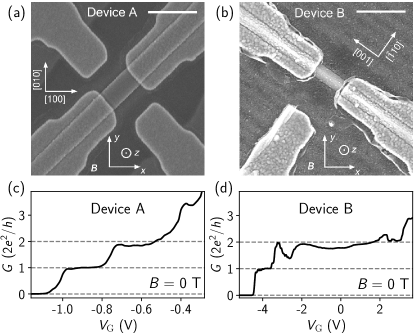
Figures 1(a) and 1(b) illustrate scanning electron micrographs (SEMs) of two devices, denoted as A and B. The PbTe nanowires were selectively grown on a CdTe substrate [28]. A thin insulating layer of Pb1-xEuxTe was grown prior to the PbTe growth, which could suppress disorder [48]. The value of is estimated to be 0.08 for device A and 0.07 for device B. The substrate of device A is CdTe(001) while for device B it is CdTe(110). After the PbTe growth, a thin layer of Pb1-xEuxTe (CdTe) was capped for device A (B) to prevent oxidization. Ohmic contacts and side gates were deposited via the evaporation of Ti/Au. The thickness of Ti is 10 nm, and for Au it is 55 (75) nm for device A (B). The two side gates of device A were interconnected during the measurement.
The linear conductance as a function of the gate voltage () for both devices exhibits quantized plateaus, as shown in Figs. 1(c-d). = 0 T. These measurements were performed in a dilution refrigerator operating at its base temperature ( 50 mK). Standard two-terminal circuit was used to obtain the device differential conductance, . The bias voltage between the two contacts was fixed to zero. The line-resistance, mainly contributed by the fridge filters, was subtracted. Contact resistances of 900 for device A and 500 for device B were estimated (and subtracted) based on the plateau values.
The zero-field plateaus are in steps of , indicating the lifting of valley degeneracy in PbTe nanowires on both (001) and (110) substrates. The pre-factor of 2 originates from spin degeneracy. Earlier numerical calculations had suggested a two-fold valley degeneracy along these crystal orientations [27]. Our recent work has indeed confirmed this two-fold degeneracy by observing plateaus at high magnetic fields along the same orientation as device A [34]. In the current study, we have reduced the wire thickness to 40 nm for device A (as opposed to 100 nm in our previous work [34]). We thus attribute the lifting of valley degeneracy in device A to a stronger confinement. For device B, the nanowire top surface is triangle-like. Note that the valley degeneracy could be lifted by device asymmetry due to the capping/substrate layer, the side mask or a side gate.
Conductance oscillations are present and superimposed on the plateaus of device B in Fig. 1(d). The oscillation amplitudes are large for the second plateau and small for the first one. We ascribe the small oscillations on the first plateau to be Fabry-Pérot-induced, a phenomenon typical in QPCs with sharp confinement potentials [49]. The large modulations on the second plateau likely arise from a quasi-bound state, which will be discussed later.
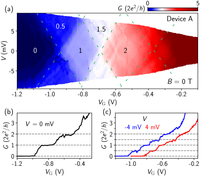
To reveal the sizes of subband spacing, Fig. 2(a) shows the 2D conductance map, vs and . For the waterfall and transconductance plots of Fig. 2(a), see Fig. S1 in the Supplemental Material. The zero-bias plateaus are now revealed as diamond shapes within which the conductance remains nearly constant. The diamond values are labeled in units of . The diamond boundaries (dashed lines) correspond to the alignment of the quasi-fermi levels in the source/drain contacts with each subband. The sizes of the diamonds thus provide a direct measurement of the energy spacing between subbands. We estimate the spacing between the second subband () and the first one () to be 8.3 meV. Likewise, the spacing 9.6 meV can also be estimated, with denoting the third subband. Moreover, the half plateaus at finite bias correspond to situations in which the quasi-fermi levels of the source and drain contacts are positioned within different subbands. Line cuts at both zero and finite bias for integer and half plateaus are shown in Figs. 2(b-c).
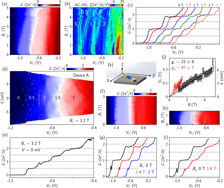
Next we study the dependence of these plateaus. Figure 3(a) shows the scan along the axis, which is perpendicular to the nanowire (out-of-plane). The coordinate axes are drawn in the middle panel of Fig. 3 (also labeled in Fig. 1(a)). As is increased, the and plateaus gradually emerge and expand from the and plateaus. These half plateaus (in units of ) arise due to the Zeeman splitting of subbands. The transconductance, in Fig. 3(b), can better illustrate this evolution, see also Fig. 3(c) for line cuts.
Figure 3(d) presents the 2D scan of vs and with being fixed at 3.2 T. The dashed lines highlight the plateau diamonds, with labeled values provided in units of . For the waterfall and transconductance plots, see Fig. S1. The zero-bias line cut in Fig. 3(e) illustrates the plateaus, accompanied by charge jumps, e.g. near = -0.9 V. The charge jump occurred swiftly (within a single pixel of the color map), leading to a sharp conductance drop. Obviously, this re-entrance behavior is not the signature of a helical gap.
Figures 3(f-i) are the scans along two other directions. The range is limited by hardware. The small peaks below the first plateau are charge jumps. Notably, the plateau is already well developed for = 1.4 T (the red curve in Fig. 3(i)). As a contrast, this half plateau is absent for at the same field (the red curve in Fig. 3(g)), and also barely visible for at an even higher field of 2 T (the blue curve in Fig. 3(c)). This anisotropic behavior indicates variations in the Landé -factor for different directions.
In Fig. 3(j) we extract the width of the plateau as a function of along the and axes. The width is estimated based on the spacing between the black dots (peaks in the transcodnuctance) in Figs. 3(b) and S1(f). The scan does not reveal the plateau at the highest applied field (3 T), thus not presented. The plateau width in is converted to energy based on the lever arm extracted from Fig. 2(a). This energy corresponds to the Zeeman splitting . is the Bohr magneton and the arrows denote spins. The slopes of the linear fits give a -factor of 23 8 for and 47 7 for . Note that the presence of a charge jump near plateau may lead to a slight overestimate of the corresponding -factor. For the analysis of other plateaus and the corresponding -factors, see Fig. S1. The -factor anisotropy in nanowires is widely present [31] and depends on various factors such as confinement and crystal direction [27, 50].
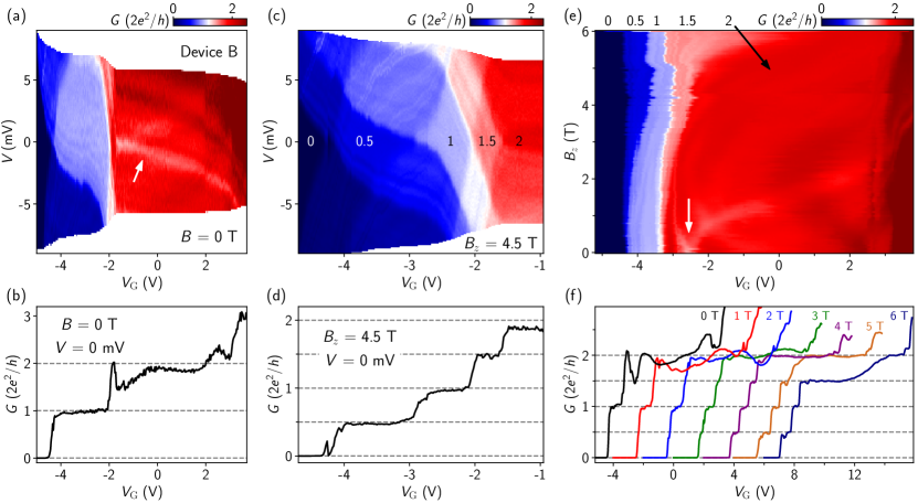
Figure 4 shows a second device (device B) that exhibits ballistic transport. The first plateau appears as a twisted diamond in Fig. 4(a). This twist implies a non-linear crosstalk between bias and gate voltages. The origin of this crosstalk is currently unknown. The size of the diamond suggests a subband spacing 8 meV. The second plateau in Fig. 4(b) is severely modulated by a quasi-bound state, a resonant level formed by weak scattering within the device. Its energy is gate tunable, see the white arrow in Fig. 4(a). These resonant-induced oscillations can mimic the re-entrance behavior characteristic of a helical gap [47].
At = 4.5 T, the first four spin-resolved plateaus, in steps of , are clearly revealed in Figs. 4(c-d). The diamonds of the 0.5 and 1 plateaus (in units of ) also exhibit a twisted shape. The plateau in Fig. 4(d) is slightly lower than the quantized value, suggesting a non-unity transmission for that particular subband. We estimate a -factor of 15 based on the size of the 0.5 plateau ( 4 meV). Fabry-Pérot-like oscillations are visible within the plateau diamonds in Fig. 4(c), suggesting a sharp QPC constriction potential [49].
In Fig. 4(e) we show the evolution of the plateaus with line cuts shown in Fig. 4(f). The resonance level on the second plateau in Fig. 4(e) quickly splits upon increasing (see the white arrow), possibly due to Zeeman splitting. As a result, the resonant-level-induced oscillations are suppressed at higher fields, see Fig. 4(f). For the waterfall plots of Figs. 4(a) and 4(c), the transconductance of Figs. 4(a), 4(c) and 4(e), and the -factor estimations, see Fig. S2 in the Supplemental Material.
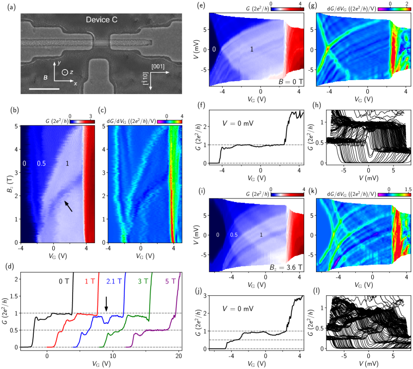
We further present a third ballistic device (device C), see the SEM in Fig. 5(a). The substrate is CdTe(110). Figures 5(b-d) illustrate the scan, the transconductance plot and line cuts. A contact resistance of 1.1 k was subtracted. The plateau is clearly revealed at zero field. The absence of the plateau indicates valley or orbital degeneracy of the second subband. As is increased, the plateau emerges and expands due to Zeeman splitting.
Notably, an additional dip feature (see the arrow in Figs. 5(b) and 5(d)) also develops on the plateau. The blue line cut in Fig. 5(d) depicts this drop, a re-entrance of conductance, on the plateau. This re-entrance behavior, obviously not a charge jump, is reminiscent of a helical gap. For a continuous evolution of the dip, see all the line cuts ( from 0 T to 4 T) of this feature in Fig. S3. The and scans, also shown in Fig. S3, do not reveal this re-entrance signature, possibly due to the -factor anisotropy. The dip does not reach , while a conductance dip of is expected in the ideal situation of a helical gap. Furthermore, the dip bends towards higher energy (more positive ) for higher , where in the simplest helical gap model, the re-entrance dip should gradually merge toward the plateau. These deviations suggest that either the observation does not arise from a helical gap or a more sophisticated helical gap model is required. Unlike III-V semiconductors, the highly anisotropic properties of PbTe does lead to a complicated situation, e.g. could also induce Zeeman splitting for spins along and axis, as the -factor in PbTe is a tensor [27] and may be dependent. More theory inputs and experimental studies in more devices with different wire geometries and orientations are required before one can conclude on the origin of this re-entrance observation.
Figures 5(e-h) show the 2D map of the first plateau, the transconductance and the waterfall plots at zero field while Figs. 5(i-l) are for = 3.6 T. The diamond size in Fig. 5(e) suggests a subband spacing 8.7 meV. Fabry-Pérot oscillations are present and superimposed on the plateau diamonds, shown in Figs. 5(e) and 5(g). The first plateau in Fig. 5(f) is revealed as clusters of curves near in the waterfall plots in Fig. 5(h). The clusters at high biases, e.g. 5 mV, are the fractional plateaus. The fractional values are not exactly half, probably due to the asymmetry of the device circuit. The lock-in excitation () is not equally shared between the quasi-fermi levels of the source and drain contacts. The diamond size of the 0.5 plateau in Fig. 5(i) is 3.2 meV, indicating a -factor of 15. Besides the three devices (A-C), Figs. S4-S6 present three additional devices that exhibit signatures of ballistic transport at zero field.
In summary, we have observed quantized conductance plateaus in units of at zero magnetic field in PbTe nanowires. The plateau values indicate the lifting of valley degeneracy in PbTe. At finite magnetic fields, half plateaus can be observed due to Zeeman splitting. Landé -factor can be extracted and its anisotropy has been discussed. A conductance dip on the plateau is observed in one device, reminiscent of (also with deviations from) the possible re-entrance behavior of a helical gap. These ballistic PbTe nanowire devices represent an improvement on diminishing disorder in SAG nanowires, which may advance the Majorana research and the search of spin-orbit helical gaps.
I Acknowledgment
We thank Leo Kouwenhoven for valuable discussions. This work is supported by Tsinghua University Initiative Scientific Research Program, National Natural Science Foundation of China (92065206) and the Innovation Program for Quantum Science and Technology (2021ZD0302400).
II Data Availability
Raw data and processing codes within this paper are available at https://doi.org/10.5281/zenodo.8336920
References
- Pan and Das Sarma [2020] H. Pan and S. Das Sarma, Physical mechanisms for zero-bias conductance peaks in Majorana nanowires, Phys. Rev. Research 2, 013377 (2020).
- Lutchyn et al. [2010] R. M. Lutchyn, J. D. Sau, and S. Das Sarma, Majorana fermions and a topological phase transition in semiconductor-superconductor heterostructures, Phys. Rev. Lett. 105, 077001 (2010).
- Oreg et al. [2010] Y. Oreg, G. Refael, and F. von Oppen, Helical liquids and Majorana bound states in quantum wires, Phys. Rev. Lett. 105, 177002 (2010).
- Chang et al. [2015] W. Chang, S. Albrecht, T. Jespersen, F. Kuemmeth, P. Krogstrup, J. Nygård, and C. M. Marcus, Hard gap in epitaxial semiconductor–superconductor nanowires, Nature Nanotechnology 10, 232 (2015).
- Krogstrup et al. [2015] P. Krogstrup, N. Ziino, W. Chang, S. Albrecht, M. Madsen, E. Johnson, J. Nygård, C. Marcus, and T. Jespersen, Epitaxy of semiconductor–superconductor nanowires, Nature Materials 14, 400 (2015).
- Kammhuber et al. [2016] J. Kammhuber, M. C. Cassidy, H. Zhang, Ö. Gül, F. Pei, M. W. de Moor, B. Nijholt, K. Watanabe, T. Taniguchi, D. Car, et al., Conductance quantization at zero magnetic field in InSb nanowires, Nano Letters 16, 3482 (2016).
- Gül et al. [2017] Ö. Gül, H. Zhang, F. K. de Vries, J. van Veen, K. Zuo, V. Mourik, S. Conesa-Boj, M. P. Nowak, D. J. van Woerkom, M. Quintero-Pérez, et al., Hard superconducting gap in InSb nanowires, Nano Letters 17, 2690 (2017).
- Zhang et al. [2017] H. Zhang, Ö. Gül, S. Conesa-Boj, M. P. Nowak, M. Wimmer, F. K. De Vries, J. Van Veen, M. W. De Moor, et al., Ballistic superconductivity in semiconductor nanowires, Nature Communications 8, 16025 (2017).
- Mourik et al. [2012] V. Mourik, K. Zuo, S. M. Frolov, S. Plissard, E. P. Bakkers, and L. P. Kouwenhoven, Signatures of Majorana fermions in hybrid superconductor-semiconductor nanowire devices, Science 336, 1003 (2012).
- Deng et al. [2016] M. Deng, S. Vaitiekėnas, E. B. Hansen, J. Danon, M. Leijnse, K. Flensberg, J. Nygård, P. Krogstrup, and C. M. Marcus, Majorana bound state in a coupled quantum-dot hybrid-nanowire system, Science 354, 1557 (2016).
- Gül et al. [2018] Ö. Gül, H. Zhang, J. D. Bommer, M. W. de Moor, D. Car, S. R. Plissard, E. P. Bakkers, A. Geresdi, K. Watanabe, T. Taniguchi, et al., Ballistic Majorana nanowire devices, Nature Nanotechnology 13, 192 (2018).
- Song et al. [2022] H. Song, Z. Zhang, D. Pan, D. Liu, Z. Wang, Z. Cao, L. Liu, L. Wen, D. Liao, R. Zhuo, D. E. Liu, R. Shang, J. Zhao, and H. Zhang, Large zero bias peaks and dips in a four-terminal thin InAs-Al nanowire device, Phys. Rev. Research 4, 033235 (2022).
- Zhang et al. [2019] H. Zhang, D. E. Liu, M. Wimmer, and L. P. Kouwenhoven, Next steps of quantum transport in Majorana nanowire devices, Nature Communications 10, 5128 (2019).
- Prada et al. [2020] E. Prada, P. San-Jose, M. W. de Moor, A. Geresdi, E. J. Lee, J. Klinovaja, D. Loss, J. Nygård, R. Aguado, and L. P. Kouwenhoven, From Andreev to Majorana bound states in hybrid superconductor–semiconductor nanowires, Nature Reviews Physics 2, 575 (2020).
- Cao et al. [2023] Z. Cao, S. Chen, G. Zhang, and D. E. Liu, Recent progress on Majorana in semiconductor-superconductor heterostructures–engineering and detection, Sci. China-Phys. Mech. Astron. 66, 267003 (2023).
- Wang et al. [2022] Z. Wang, H. Song, D. Pan, Z. Zhang, W. Miao, R. Li, Z. Cao, G. Zhang, L. Liu, L. Wen, R. Zhuo, D. E. Liu, K. He, R. Shang, J. Zhao, and H. Zhang, Plateau regions for zero-bias peaks within 5 of the quantized conductance value , Phys. Rev. Lett. 129, 167702 (2022).
- Dvir et al. [2023] T. Dvir, G. Wang, N. Loo, C.-X. Liu, G. Mazur, A. Bordin, S. Haaf, J.-Y. Wang, D. Driel, F. Zatelli, et al., Realization of a minimal Kitaev chain in coupled quantum dots, Nature 614, 445 (2023).
- Aghaee et al. [2023] M. Aghaee, A. Akkala, Z. Alam, R. Ali, A. Alcaraz Ramirez, M. Andrzejczuk, A. E. Antipov, P. Aseev, M. Astafev, B. Bauer, et al. (Microsoft Quantum), Inas-al hybrid devices passing the topological gap protocol, Phys. Rev. B 107, 245423 (2023).
- Banerjee et al. [2023] A. Banerjee, O. Lesser, M. A. Rahman, H.-R. Wang, M.-R. Li, A. Kringhøj, A. M. Whiticar, A. C. C. Drachmann, C. Thomas, T. Wang, et al., Signatures of a topological phase transition in a planar Josephson junction, Phys. Rev. B 107, 245304 (2023).
- Wharam et al. [1988] D. A. Wharam, T. J. Thornton, R. Newbury, M. Pepper, H. Ahmed, J. E. F. Frost, D. G. Hasko, D. C. Peacock, D. A. Ritchie, and G. A. C. Jones, One-dimensional transport and the quantisation of the ballistic resistance, Journal of Physics C: Solid State Physics 21, L209 (1988).
- van Wees et al. [1988] B. J. van Wees, H. van Houten, C. W. J. Beenakker, J. G. Williamson, L. P. Kouwenhoven, D. van der Marel, and C. T. Foxon, Quantized conductance of point contacts in a two-dimensional electron gas, Phys. Rev. Lett. 60, 848 (1988).
- Liu et al. [2012] J. Liu, A. C. Potter, K. T. Law, and P. A. Lee, Zero-bias peaks in the tunneling conductance of spin-orbit-coupled superconducting wires with and without Majorana end-states, Phys. Rev. Lett. 109, 267002 (2012).
- Pikulin et al. [2012] D. I. Pikulin, J. P. Dahlhaus, M. Wimmer, H. Schomerus, and C. W. J. Beenakker, A zero-voltage conductance peak from weak antilocalization in a Majorana nanowire, New Journal of Physics 14, 125011 (2012).
- Rainis et al. [2013] D. Rainis, L. Trifunovic, J. Klinovaja, and D. Loss, Towards a realistic transport modeling in a superconducting nanowire with Majorana fermions, Physical Review B 87, 024515 (2013).
- Das Sarma and Pan [2021] S. Das Sarma and H. Pan, Disorder-induced zero-bias peaks in Majorana nanowires, Phys. Rev. B 103, 195158 (2021).
- Zeng et al. [2022] C. Zeng, G. Sharma, S. Tewari, and T. Stanescu, Partially separated Majorana modes in a disordered medium, Phys. Rev. B 105, 205122 (2022).
- Cao et al. [2022] Z. Cao, D. E. Liu, W.-X. He, X. Liu, K. He, and H. Zhang, Numerical study of PbTe-Pb hybrid nanowires for engineering Majorana zero modes, Phys. Rev. B 105, 085424 (2022).
- Jiang et al. [2022] Y. Jiang, S. Yang, L. Li, W. Song, W. Miao, B. Tong, Z. Geng, Y. Gao, R. Li, F. Chen, Q. Zhang, F. Meng, L. Gu, K. Zhu, Y. Zang, R. Shang, Z. Cao, X. Feng, Q.-K. Xue, D. E. Liu, H. Zhang, and K. He, Selective area epitaxy of PbTe-Pb hybrid nanowires on a lattice-matched substrate, Phys. Rev. Materials 6, 034205 (2022).
- Jung et al. [2022] J. Jung, S. G. Schellingerhout, M. F. Ritter, S. C. ten Kate, O. A. van der Molen, S. de Loijer, M. A. Verheijen, H. Riel, F. Nichele, and E. P. Bakkers, Selective area growth of PbTe nanowire networks on InP, Advanced Functional Materials 32, 2208974 (2022).
- Geng et al. [2022] Z. Geng, Z. Zhang, F. Chen, S. Yang, Y. Jiang, Y. Gao, B. Tong, W. Song, W. Miao, R. Li, Y. Wang, Q. Zhang, F. Meng, L. Gu, K. Zhu, Y. Zang, L. Li, R. Shang, X. Feng, Q.-K. Xue, K. He, and H. Zhang, Observation of Aharonov-Bohm effect in PbTe nanowire networks, Phys. Rev. B 105, L241112 (2022).
- ten Kate et al. [2022] S. C. ten Kate, M. F. Ritter, A. Fuhrer, J. Jung, S. G. Schellingerhout, E. P. A. M. Bakkers, H. Riel, and F. Nichele, Small charging energies and g-factor anisotropy in PbTe quantum dots, Nano Letters 22, 7049 (2022).
- Zhang et al. [2023] Z. Zhang, W. Song, Y. Gao, Y. Wang, Z. Yu, S. Yang, Y. Jiang, W. Miao, R. Li, F. Chen, Z. Geng, Q. Zhang, F. Meng, T. Lin, L. Gu, K. Zhu, Y. Zang, L. Li, R. Shang, X. Feng, Q.-K. Xue, K. He, and H. Zhang, Proximity effect in PbTe-Pb hybrid nanowire Josephson junctions, Phys. Rev. Mater. 7, 086201 (2023).
- Gao et al. [2023] Y. Gao, W. Song, S. Yang, Z. Yu, R. Li, W. Miao, Y. Wang, F. Chen, Z. Geng, L. Yang, et al., Hard superconducting gap in PbTe nanowires, arXiv: 2309.01355 (2023).
- Song et al. [2023] W. Song, Y. Wang, W. Miao, Z. Yu, Y. Gao, R. Li, S. Yang, F. Chen, Z. Geng, Z. Zhang, S. Zhang, Y. Zang, Z. Cao, D. E. Liu, R. Shang, X. Feng, L. Li, Q.-K. Xue, K. He, and H. Zhang, Conductance quantization in PbTe nanowires, Phys. Rev. B 108, 045426 (2023).
- Abay et al. [2013] S. Abay, D. Persson, H. Nilsson, H. Xu, M. Fogelström, V. Shumeiko, and P. Delsing, Quantized conductance and its correlation to the supercurrent in a nanowire connected to superconductors, Nano Letters 13, 3614–3617 (2013).
- Gooth et al. [2017] J. Gooth, M. Borg, H. Schmid, V. Schaller, S. Wirths, K. Moselund, M. Luisier, S. Karg, and H. Riel, Ballistic one-dimensional InAs nanowire cross-junction interconnects, Nano Letters 17 (2017).
- Estrada Saldana et al. [2018] J. C. Estrada Saldana, Y.-M. Niquet, J.-P. Cleuziou, E. Lee, D. Car, S. Plissard, E. Bakkers, and S. Franceschi, Split-channel ballistic transport in an InSb nanowire, Nano Letters 18, 2282 (2018).
- Vaitiekėnas et al. [2018] S. Vaitiekėnas, A. M. Whiticar, M.-T. Deng, F. Krizek, J. E. Sestoft, C. J. Palmstrøm, S. Marti-Sanchez, J. Arbiol, P. Krogstrup, L. Casparis, and C. M. Marcus, Selective-area-grown semiconductor-superconductor hybrids: A basis for topological networks, Phys. Rev. Lett. 121, 147701 (2018).
- Friedl et al. [2018] M. Friedl, K. Cerveny, P. Weigele, G. Tutuncuoglu, S. Martí-Sánchez, C. Huang, T. Patlatiuk, H. Potts, Z. Sun, M. Hill, et al., Template-assisted scalable nanowire networks, Nano Letters 18, 2666 (2018).
- Lee et al. [2019] J. S. Lee, S. Choi, M. Pendharkar, D. J. Pennachio, B. Markman, M. Seas, S. Koelling, M. A. Verheijen, L. Casparis, K. D. Petersson, et al., Selective-area chemical beam epitaxy of in-plane InAs one-dimensional channels grown on InP(001), InP(111)b, and InP(011) surfaces, Phys. Rev. Mater. 3, 084606 (2019).
- Aseev et al. [2019] P. Aseev, G. Wang, L. Binci, A. Singh, S. Martí-Sánchez, M. Botifoll, L. Stek, A. Bordin, J. Watson, F. Boekhout, et al., Ballistic InSb nanowires and networks via metal-sown selective area growth, Nano Letters 19, 9102 (2019).
- het Veld et al. [2020] R. L. M. O. het Veld, D. Xu, V. Schaller, M. A. Verheijen, S. M. E. Peters, J. Jung, C. Tong, Q. Wang, M. W. A. de Moor, B. Hesselmann, et al., In-plane selective area InSb–Al nanowire quantum networks, Communications Physics 3, 59 (2020).
- Pershin et al. [2004] Y. V. Pershin, J. A. Nesteroff, and V. Privman, Effect of spin-orbit interaction and in-plane magnetic field on the conductance of a quasi-one-dimensional system, Phys. Rev. B 69, 121306 (2004).
- Quay et al. [2009] C. Quay, T. Hughes, J. Sulpizio, L. Pfeiffer, K. Baldwin, K. West, D. Goldhaber-Gordon, and R. de Picciotto, Observation of a one-dimensional spin-orbit gap in a quantum wire, Nature Physics 6, 336 (2009).
- Kammhuber et al. [2017] J. Kammhuber, C. Cassidy, F. Pei, M. Nowak, A. Vuik, D. Car, S. Plissard, E. Bakkers, M. Wimmer, and L. Kouwenhoven, Conductance through a helical state in an InSb nanowire, Nature Communications 8, 478 (2017).
- Heedt et al. [2017] S. Heedt, N. Traverso Ziani, F. Crépin, W. Prost, S. Trellenkamp, J. Schubert, D. Grützmacher, B. Trauzettel, and T. Schäpers, Signatures of interaction-induced helical gaps in nanowire quantum point contacts, Nature Physics 13, 563 (2017).
- Rainis and Loss [2014] D. Rainis and D. Loss, Conductance behavior in nanowires with spin-orbit interaction: A numerical study, Phys. Rev. B 90, 235415 (2014).
- Huang and Shklovskii [2021] Y. Huang and B. I. Shklovskii, Disorder effects in topological insulator nanowires, Phys. Rev. B 104, 054205 (2021).
- Maao/ et al. [1994] F. A. Maao/, I. V. Zozulenko, and E. H. Hauge, Quantum point contacts with smooth geometries: Exact versus approximate results, Phys. Rev. B 50, 17320 (1994).
- Pryor and Flatté [2006] C. E. Pryor and M. E. Flatté, Landé factors and orbital momentum quenching in semiconductor quantum dots, Phys. Rev. Lett. 96, 026804 (2006).
See pages 1 of PbTe_Ballistic_SM.pdf See pages 2 of PbTe_Ballistic_SM.pdf See pages 3 of PbTe_Ballistic_SM.pdf See pages 4 of PbTe_Ballistic_SM.pdf See pages 5 of PbTe_Ballistic_SM.pdf See pages 6 of PbTe_Ballistic_SM.pdf