Data Acquisition System for the CALICE AHCAL Calorimeter
Abstract
The data acquisition system (DAQ) for a highly granular analogue hadron calorimeter (AHCAL) for the future International Linear Collider is presented. The developed DAQ chain has several stages of aggregation and scales up to 8 million channels foreseen for the AHCAL detector design. The largest aggregation device, Link Data Aggregator, has 96 HDMI connectors, four Kintex7 FPGAs and a central Zynq System-On-Chip. Architecture and performance results are shown in detail. Experience from DESY testbeams with a small detector prototype consisting of 15 detector layers are shown.
1 Introduction
The international CALICE collaboration [1] is developing calorimeters for detectors at future linear electron-positron colliders with a very high granularity, which is essential for the particle flow reconstruction algorithm [2] to achieve the best jet energy resolution. The AHCAL (Analog Hadron CALorimeter) group is developing a steel sandwich hadron calorimeter option, that uses scintillating tiles for light conversion and SiPM (Silicon Photo-Multipliers) detectors for reading out each tile individually. This granularity corresponds to in total 8 million channels in the AHCAL barrel and endcaps.
The data acquisition (DAQ) concept needs to cope with such granularity by defining aggregation stages. The DAQ concept [3, 4] that was proposed for calorimeters for ILD (International Large Detector, [5]) is scalable to the final detector system. The first generation CALICE prototypes used the same DAQ system in beam tests. Since then, the DAQ systems have been individually adapted for the technological prototypes. The current AHCAL DAQ, which utilizes data concentration electronics, is also used by the scintillator-based ECAL (Electromagnetic Calorimeter) prototype.
The AHCAL DAQ serves two distinct purposes: it provides a) a stable DAQ usable for tests of the detector prototypes in the lab and in beam tests; b) a technological demonstrator of a DAQ, that can be scaled to the final detector system and ILC (International Linear Collider) timing.
2 Architecture
The architecture reflects the timing of the ILC accelerator and power constraints given by the ILD. The timing requirements are specific to the ILC, where the collisions take place in a train of bunches spaced apart, followed by idle time. The power constraints reflect the lack of active cooling within detector volume in the AHCAL design [5], where the temperature difference between the cooled sides and the center limits the average power dissipation of a single channel to per channel, when a geometry is considered.
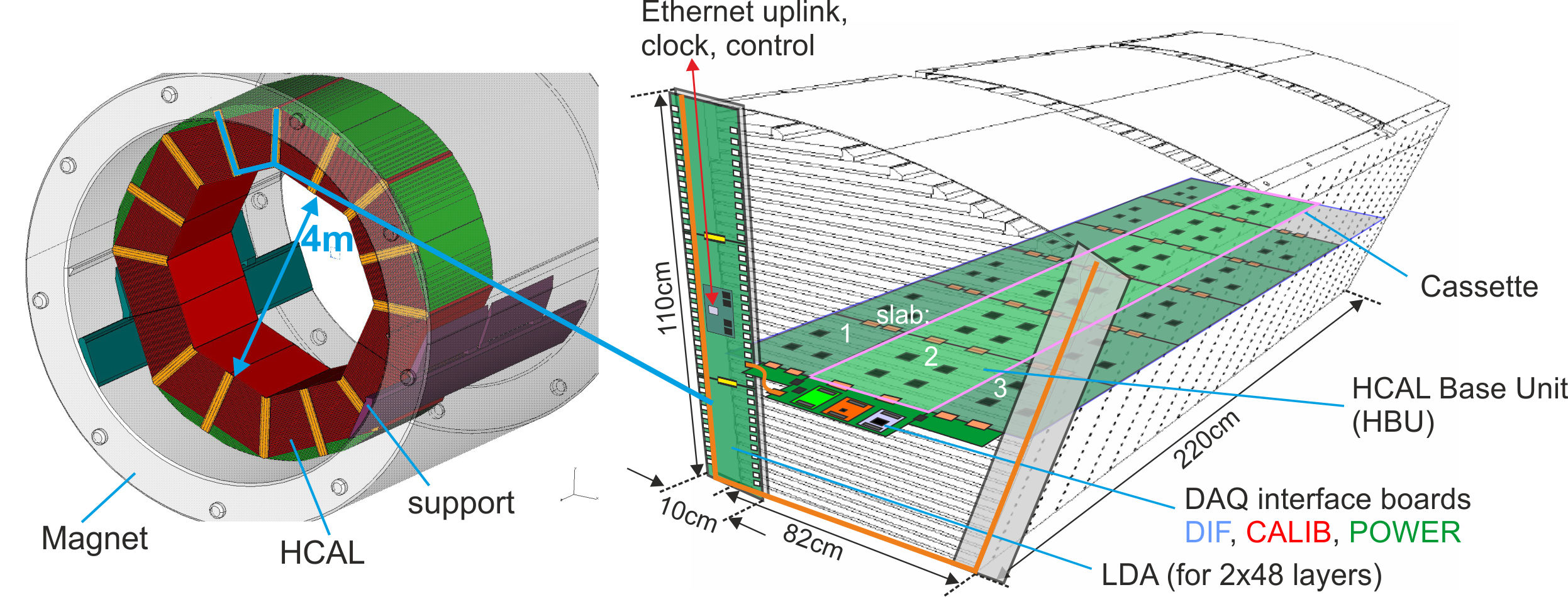
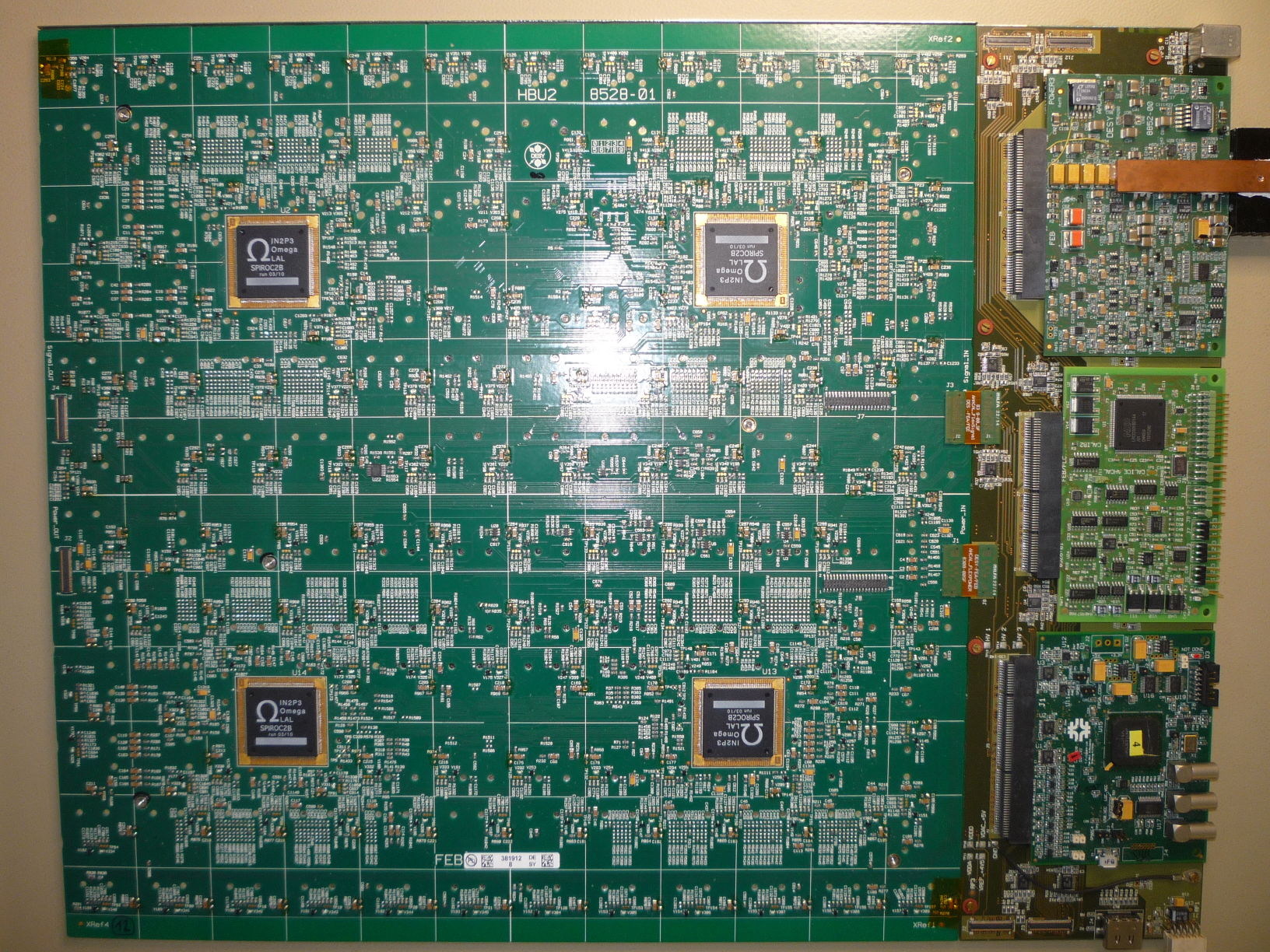
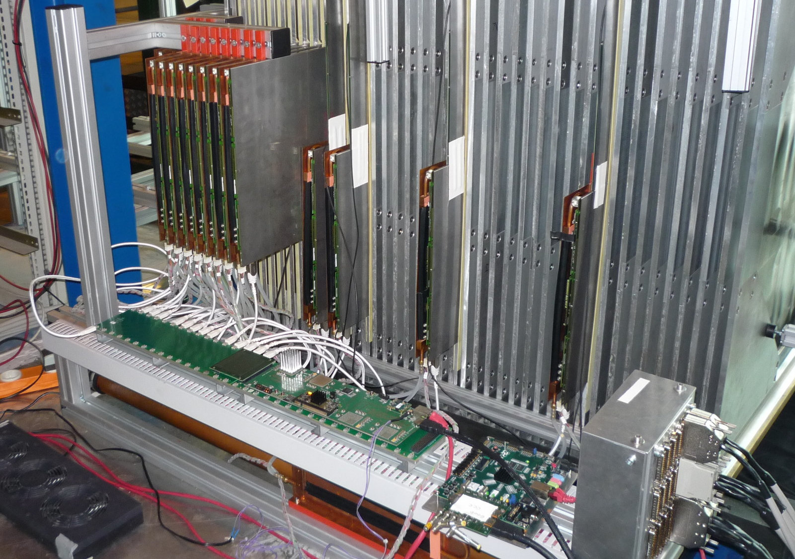
The electronics geometry is limited by a gap between absorber material, which has to contain a thick plastic scintillating tile with SiPM detector, a thinned PCB and for SMD components and connectors. The active electronics and detection layer spans along the barrel (figure 1 (left)), and is segmented into HBUs (AHCAL base units, figure 1 (right)) with size.
To achieve low power dissipation, the acquisition cycle is split in 3 phases, shown in figure 2:
-
1.
The acquisition phase, where the electrical signal is saved in the form of charge in analog memory cells in the very front-end ASICs. A zero suppression is applied by a self-triggered operation.
-
2.
The conversion phase, where all stored analogue signals are converted to digital signals by a single ADC integrated into the very front-end ASIC.
-
3.
The readout phase, where the data is shifted out from the ASICs further in the DAQ chain. The data bus is shared among 12 ASICs in the readout chain.
Each phase has independent power control, where the power is enabled only for the preamplifiers in the acquisition phase, the ADC is enabled only in the conversion phase and the digital part is enabled only in the readout phase.
2.1 Hierarchy
The AHCAL DAQ architecture adopted the aggregation hierarchy from the DAQ concept [3], but the hardware was developed from scratch. The aggregation factors are shown in figure 3. The following list describes the individual components in the DAQ chain:
- SPIROC
-
is an ASIC developed by the Omega group [6], which has 36 input channels, an 0SCA (Switched Capacitor Array) for storing up to 16 events in analog form and an integrated 12-bit ADC. Charge (ADC) and Time (TDC) information is stored for each channel independently. Only signals passing a programmable threshold are stored.
- HBU (AHCAL Base Unit)
- DIF (Detector InterFace)
-
is the first aggregation component, which controls and reads out up to 3 slabs, which corresponds to 18 HBUs or 72 ASICs. The data is sent out via HDMI connectors with a custom serial protocol. The latest version contains a Zynq-7020 SoC (System-on-Chip), an FPGA with an embedded dual-core ARM processor [8].
- LDA (Link Data Aggregator)
- CCC (Clock_and_Control_Card)
-
delivers a beam clock to the LDA and starts the acquisition cycle with the presence of a spill. It synchronizes the clock in common beam tests of different detectors. During beam tests it also delivers a delayed trigger validation signal.
2.2 Link Data Aggregator (LDA)
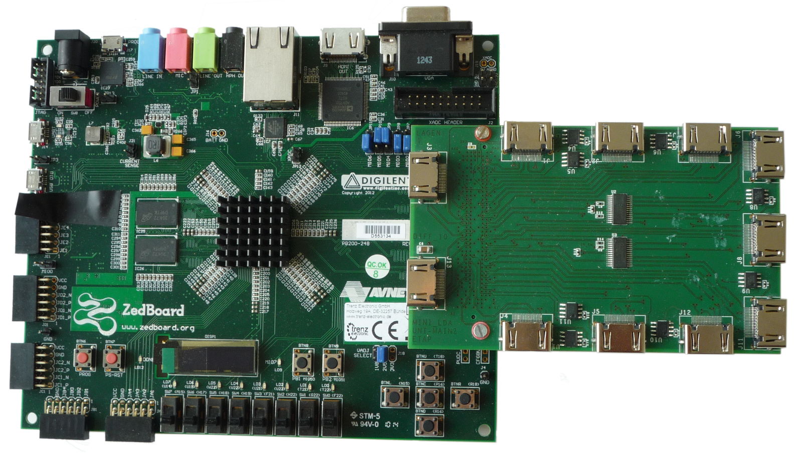
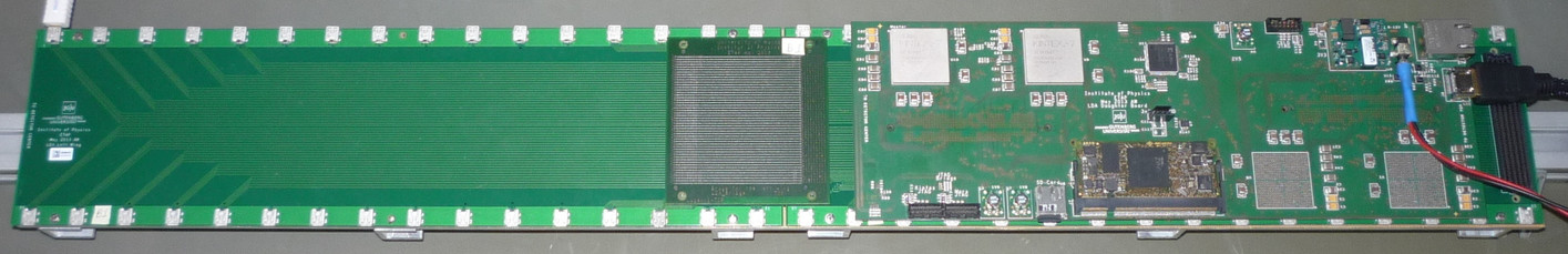
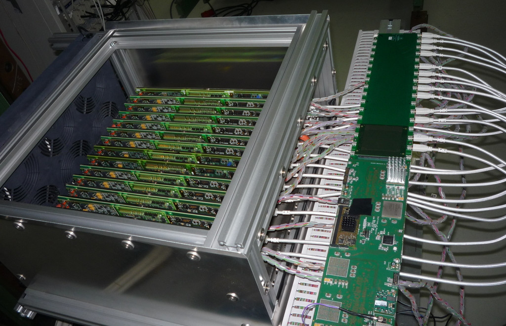
The LDA hardware exists in two form factors, that have the same functionality and are interchangeable. The Mini-LDA (figure 4 (left)) is a custom FMC-LPC (FPGA Mezzanine Card - Low Pin Count) mezzanine with 10 HDMI connectors to connect to DIFs and 1 HDMI connector to connect to CCC. The mezzanine is attached to a Zedboard, a commercial development board [9] hosting a Zynq-7020 SoC [8]. The Wing-LDA (figure 1 (right)) has in total 96 micro-HDMI ports. The connector pitch matches the AHCAL layer spacing in the barrel and the overall length of the board is , as shown in figure 1 (left). It consists of 3 passive fan-out boards with 32 micro-HDMI connectors each, that connect to an active daughter-board. The daughter-board hosts 4 Kintex-7 FPGAs (xc7k160), each serving 24 ports from passive boards. Those FPGAs are connected to a central commercial Mars ZX3 SoC module [10], which hosts the same Zynq SoC as the Mini-LDA.
The firmware of the both LDAs, Mini-LDA and Wing-LDA, share similar source code, except for the Zynq Kintex FPGA link, which splits the design into 2 FPGA partitions in the Wing-LDA form factor. The Wing-LDA FPGA firmware block diagram is shown in figure 5. The DIF sends 100-byte packet fragments to the “DIF PORT” module, where the ASIC packets are built for each SPIROC in the block memory in clock domain. Once a full ASIC packet is completed, the pointer is sent to the memory manager, which moves the data from the memory of all “DIF PORTS” to a large buffer, from where it is transported over the AXI-stream [11] infrastructure.
The “FPGA link” module has a circular buffer for up to 8 packets. A CRC-16 check-sum is added for each packet. Two bytes are encoded using the 8b10b code and serialized in clock domain in DDR mode, providing a dual link in each direction. The check-sum of received packets is checked and in case of error the packet is re-transmitted up to 3 times. Control words (transmit succeed or fail, buffer full) are interleaved in the stream via dedicated 8b10b control symbols. Fast commands from the CCC (start and stop acquisition, synchronization) are also transmitted as dedicated control symbols with highest priority, maintaining a consistent command propagation delay.
Packets from the AXI-stream FIFO are moved to the DDR memory using an AXI DMA (Direct Memory Access) core in a simple transaction mode (scatter-gather engine not used). Packet boundaries are omitted in the DMA transfer in order to minimize the overhead of initiating the transfer. The DMA is initiated using a custom written Linux kernel module, which makes received data accessible via a Linux character device. The processor part of the Zynq SoC is running a Petalinux Linux distribution [12] on both cores and hosts a simple TCP server, that streams all data from the character device.
2.3 Speed and data volume consideration
The data volumes are shown at figure 3. The SPIROC produces packets depending on how many of up to 16 events were stored in the acquisition phase. The LED light calibration fills all memory cells of all SPIROCs and uses the maximum of the data volume per readout cycle and defines the minimum required bandwidth for the DAQ, which is per LDA per readout cycle. This corresponds to for the ILD geometry and accelerator repetition frequency of .
Data from all SPIROCs has to be readout within before the next acquisition cycle starts. For 6 HBUs in a slab, which corresponds to 24 SPIROCs in two shared readout chain buses, the minimum transfer speed is . A readout speed is currently implemented. The SPIROC itself specifies a readout clock frequency limit. Similarly, a DIF has to send up to data chunks with a speed at least . The currently used serial protocol uses a clock, providing bandwidth.
The LDA needs to be able to supply continuously over a GbE port. This requirement is close to the Ethernet bandwidth limit during the LED calibration and might get replaced for the final detector in order to provide bandwidth overhead.
Since the LDA will be the device with the largest data traffic, it has been subjected to bandwidth benchmarking. The FPGAs internally process the data from the DIFs with . The link between the FPGAs of a Wing-LDA is capable of transferring nearly for each slave FPGA and the further processing in the central FPGA has a limit. The speed of the DMA transfer to the processor memory depends on the size of the packets being moved by the DMA IP core and the size of the buffer used for reading from the character device, as shown in figure 6. The maximum transfer speed of is achieved when a read buffer is used and small packets are merged into chunks in the FPGA.
The software part in the SoC, which only sends the data from the memory to the TCP socket, does not yet reach the requested bandwidth. The maximum data transfer rate over the TCP was measured to be only , one order of magnitude below the requirements.
It is not foreseen, that the current Linux TCP socket implementation will be used in the final detector installation. It will be replaced for the final detector. The overall TCP performance is enough for serving the beam tests with the currently available layers without hitting the bandwidth limit, but will need to be optimized for larger prototypes, especially when the spill rate will be higher than the expected at the ILC.
3 Beam test operation and performance
Testbeam facilities have typically very different timing to the ILC accelerator, which is expected to have spills with repetition rate, resulting in a duty cycle. However, testbeam facilities typically have a continuous beam or rather long spills of continuous beam. Therefore, the following measures are taken, leading to an operation shown in figure 7:
-
1.
The bunch crossing period is extended from (close to of ILC) to , prolonging the acquisition window up to .
-
2.
External trigger validation is introduced, otherwise SiPM noise would become significant. Any auto-triggered event, which is not validated within the period is therefore not saved. This validation scheme is not foreseen for ILC running.
-
3.
A busy signal is raised when all 16 memory cells of a SPIROC in any layer are filled, forcing all other layers to stop. The busy is propagated through LDAs to CCC. The busy from DIFs is cleared when all data is sent out.
-
4.
Acquisition is restarted as soon as all data are sent to LDAs and LDAs have enough free space in their buffers for the next acquisition cycle.
The DAQ system in the beam test configuration has been used since the end of 2014 in many beam tests at CERN PS, CERN SPS and DESY for different layer configurations of up to 15 layers. The Wing-LDA connection to the detector layers is shown in figure 8. The performance depends primarily on the number of HBUs in the readout chain, since the transfer of data from SPIROC to DIF is the most limiting factor.
The performance depends also on the beam condition and on SiPM noise, which can be partially controlled by a trigger threshold and SiPM bias voltage. The typical performances, that have been observed during a recent beam test at DESY in 2016 are shown in table 1. The acquisition duty cycle in testbeam mode is up to two orders of magnitude higher than the designed value of , providing a possibility to efficiently record even a very low particle rate. The system was able to record up to 200 particles in the DESY test beam, which has a non-homogeneous particle burst structure.
| configuration | 22 HBUs | 11 HBU | ILC ( spill) |
|---|---|---|---|
| layers | 4 | 15 | 15 |
| SPIROCs in a layer | 16 | 4 | 4 |
| ROC | 17 | 99 | |
| duty cycle | () % | ||
| particles/s | 135 | 41 |
The ILC configuration was tested with a forced spill length maximum and bunch crossing period. The acquisition restarted as soon as possible, exceeding the expected ILC spill rate by a factor of 20.
4 Summary
The AHCAL DAQ hardware was developed with the aim of serving beam tests of the detector prototypes with the added feature of being scalable to a large ILC detector. The largest on-detector concentration device, the Wing-LDA, has been stably serving this purpose since 2014 and is already scalable to the full size of AHCAL barrel, reading out up to 8 million channels.
The DAQ functionality was demonstrated in several beam tests with up to 15 layers containing up to 108 ASIC and 3888 SiPM channels. The performance showed 200 recorded particles per second during beam tests and 450 calibrating light pulses per second during calibration. The detector duty cycle can be increased by two orders of magnitudes from the ILD duty cycle due to DAQ testbeam mode adaptations, which enable efficient data taking even in continuous, low-intensity beams.
The current hardware is able to process internally up to . The implementation of TCP server in the embedded Linux is sufficient for beam test, but does not yet meet the bandwidth requirements for the full-size detector and will have to be improved before testing even a significantly larger ( ) number of prototype layers.
Acknowledgments
The author gratefully thanks Mathew Wing, Katja Krüger, Mathias Reinecke, Eldwan Brianne, Felix Sefkow and Jaroslav Cvach for their very useful comments and feedback to this paper.
This project has received funding from the European Union’s Horizon 2020 Research and Innovation programme under Grant Agreement no. 654168.
This project has received funding from Ministry of Education, Youth and Sports of the Czech Republic under the project LG14033.
ⓒ for Figure 1 Mathias Reinecke (DESY), used with permnission of author.
References
- [1] The CALICE collaboration. https://twiki.cern.ch/twiki/bin/view/CALICE/WebHome
- [2] Thomson, M. A., Particle flow calorimetry and the PandoraPFA algorithm. Nuclear Instruments and Methods in Physics Research Section A: Accelerators, Spectrometers, Detectors and Associated Equipment. Vol 611.1 (2009): 25-40
- [3] Wing, M. et al., A proposed DAQ system for a calorimeter at the International Linear Collider, LC note, LC-DET-2006-008.
- [4] Goodrick, M.J. et al., Development of a modular and scalable data acquisition system for calorimeters at a linear collider, JINST 6 (2011) P10011.
- [5] Behnke, T. et al., The International Linear Collider Technical Design Report-Volume 4: Detectors. arXiv:1306.6329 (2013).
- [6] Di Lorenzo, S. Conforti, et al., SPIROC: design and performances of a dedicated very front-end electronics for an ILC Analog Hadronic CALorimeter (AHCAL) prototype with SiPM readout. 2013 JINST 8 C01027.
- [7] Terwort, M., Concept and status of the CALICE analog hadron calorimeter engineering prototype. Physics Procedia 37 (2012): 198-204.
- [8] https://www.xilinx.com/products/silicon-devices/soc/zynq-7000.html
- [9] http://zedboard.org/product/zedboard
- [10] http://www.enclustra.com/en/products/system-on-chip-modules/mars-zx3/
- [11] AMBA AXI4-Stream Protocol Specification v1.0, www.arm.com
- [12] http://www.xilinx.com/products/design-tools/embedded-software/petalinux-sdk.html