Dimensional crossover of charge order in IrTe2 with strong interlayer coupling
Abstract
Tuning dimensionality in van der Waals materials with finite interlayer coupling has introduced various electronic phase transitions by conventional mechanical exfoliation. Particularly when the electronic order is tied to the modulation of the interlayer coupling, such dimensional tunability has a strong impact on its stability and properties, which has rarely been investigated experimentally. Here, we demonstrate a dimensional crossover of charge order in IrTe2 from genuine two- to quasi-three-dimension using low-temperature scanning tunneling microscopy and spectroscopy. Employing atomically thin IrTe2 flakes ranging from monolayer to multilayer, we observe a gradual phase transition of charge order and exponential decay of Coulomb gap with increasing thickness. Moreover, we find a suppression of the density of states emerging at an abrupt lateral interface between two- and three-dimension. These findings are attributed to the interplay between the strongly coupled layers and substrate-driven perturbation, which can provide a new insight into the dimensional crossover of strongly coupled layered materials with hidden electronic phases.
I Introduction
Dimensionality in a quasi-two-dimensional (quasi-2D) system works as one of critical physical parameters in determining structural and electronic characteristics, which often induces various phase transitions including superconductivity Xi et al. (2016); Song et al. (2021), charge density waves Xi et al. (2015); Yu et al. (2015); Chen et al. (2022), or symmetry breaking Lin et al. (2017); Ni et al. (2021). Quasi-2D van der Waals (vdW) materials, such as transition metal dichalcogenides (TMDs), feature strong in-plane covalent bonding and weak out-of-plane vdW bonding, which enable tuning their dimensions by adjusting thickness without introducing disorder or defects Ghosh et al. (2010); Jin et al. (2013). Because a typical electronic order in vdW materials is three-dimensional (3D) due to finite interlayer coupling Yang et al. (2012); Jin et al. (2013); Yang et al. (2014), modulating out-of-plane interaction can generate fascinating layer-dependent physical properties particularly when the electronic order is strongly linked to the modulation of interlayer bonding or stacking configuration Lee et al. (2019, 2021).
IrTe2, one of exotic TMDs showing intertwined charge ordering phases, is associated by the structural phase transition from high temperature trigonal to low temperature monoclinic lattice ( K) with the wave vector of Matsumoto et al. (1999); Yang et al. (2012). Due to the intralayer Ir-Ir dimerization competing against the interlayer Te-Te bonding Machida et al. (2013); Joseph et al. (2013); Dai et al. (2014), the so-called cross-layer charge ordering with stripe charge modulations [] have been observed in the low temperature phase Hsu et al. (2013); Pascut et al. (2014). Furthermore, bulk intrinsic superconductivity emerges when the charge ordering is fully suppressed by chemical doping Yang et al. (2012); Pyon et al. (2012); Ootsuki et al. (2012); Kamitani et al. (2013) or rapid cooling Kim et al. (2016); Oike et al. (2018). In contrast to bulk IrTe2, the coexistence of superconductivity and stripe charge modulation has recently been observed in mechanically exfoliated flakes with the thickness range of 20–200 nm Park et al. (2021). Such a contrasting observation suggests that the coexisting stripe charge order significantly enhances the out-of-plane coherence length and the coupling strength of superconductivity in thin IrTe2 flakes. In this respect, IrTe2 can be a proper model system for studying the role of interlayer coupling in the interplay between charge ordering and superconductivity at different dimensions, which has not been investigated experimentally.
In this article, we have investigated atomically thin IrTe2 flakes ranging from monolayer to multilayer (up to 20 L) in order to correlate a dimensional crossover of charge order with thickness. Using the Al2O3-assisted mechanical exfoliation Deng et al. (2018), we systematically reduce the thickness of IrTe2 down to monolayer and directly probe structural and electronic properties with low temperature scanning tunneling microscopy and spectroscopy (STM/STS) measurements. We observe a gradual evolution of charge order and an exponentially decay of Coulomb gap, which have been attributed to the subtle interplay between the strong interlayer coupling and substrate-induced disorders. Furthermore, we discover an unusual depression of density of states (DOS) in empty states, which appears at an abrupt lateral interface from 2D to 3D. Our findings demonstrate that the stability of the cross-layer charge ordering and the phase competition with different ordering periods are highly sensitive to the dimensional crossover, highlighting the important role of the interlayer coupling in IrTe2.
II Method
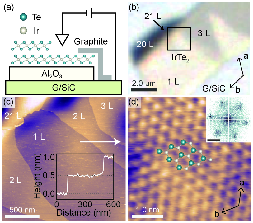
Figures 1(a) and 1(b) show our experimental setup and a typical IrTe2 flake fabricated by the Al2O3-assisted mechanical exfoliation in an inert atmosphere Deng et al. (2018) (see more details in Appendix A). We identify thicknesses of IrTe2 using optical transmission contrasts, which are highly sensitive to layer numbers of IrTe2 flakes (see Appendix B). As shown in Figs. 1(b) and 1(c), we confirm the excellent correlation between the optical contrasts and STM height profiles. Surface cleanliness, which is crucial for surface-sensitive STM, is routinely checked by room-temperature STM measurements before cooling. A typical atomic STM image of IrTe2 monolayer clearly reveals the triangular Te atomic lattice without any significant surface contamination such as vacancies or adsorbates [Fig. 1(d)]. The sample was inserted to a cooled STM stage using a continuous flow cryostat. STM/STS measurements were performed in an ultrahigh-vacuum ( Pa) cryogenic STM ( K). All STM images were recorded in the constant-current mode with an electrochemically etched W tip. STS measurements were performed by recording spectra via a lock-in technique with feedback open, using a modulation frequency of approximately 1 kHz with a root-mean-square modulation amplitude of mV.
III Result and discussion
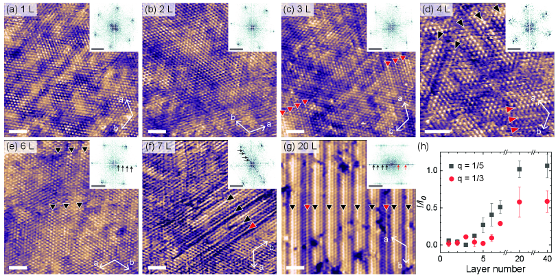
To investigate thickness-dependent charge orders, we have performed STM measurements on atomically thin IrTe2 flakes from monolayer (1 L) to multilayer up to 20 L well below the bulk transition temperature. In sharp contrast to the dimerized monolayer and bilayer IrTe2 grown by molecular beam epitaxy (MBE) on graphene Hwang et al. (2022), we found no signature of charge orders in our mechanically exfoliated monolayer and bilayer IrTe2 [Figs. 2(a) and 2(b)]. Local stripe charge orders start to emerge from trilayer (3 L) and become dominant above heptalayer (7 L) IrTe2 [Figs. 2(c)–2(g)]. To quantify the thickness dependence of the stripe charge orders, we analyze the relative peak intensities of fast Fourier transform (FFT) of charge orders with respect to Bragg peaks from atom-resolved STM images [Fig. 2(h)] Pásztor et al. (2017). To improve the reliability, we statistically averaged the relative peak intensities obtained from a sufficient number (10) of topographic images on different locations for each thickness. The charge order with the wave vector of gradually becomes stronger with increasing thickness above 3 L while the charge order exists locally on 3 L and becomes more visible above 5 L. Beyond 20 L, we found no further thickness dependence of the charge order as reported previously Park et al. (2021). This observation strongly suggests that the stripe charge order of few layer IrTe2 exhibits a gradual evolution with increasing thickness, in contrast to the abrupt metal-insulator transition between MBE-grown monolayer and bilayer IrTe2 Hwang et al. (2022).
The structural distortion and strain effect from the substrate may give rise to thickness-dependent lattice constants, which may lead to the observed thickness dependence of the charge order. To check this possibility, we have performed the quantitative analysis of the lattice constants on various thicknesses (1–20 L). Within our experimental measurement error (0.15 Å), few-layer IrTe2 on Al2O3 does not show significant thickness dependence of the lattice constants (3.65–3.82 Å). Thus, we can exclude that atomic distortion and strain effect directly from the Al2O3 substrate on the thickness dependence of the charge order.
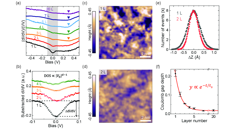
To further understand the dimensionality-induced evolution of the charge orders, we systematically probe local DOS of IrTe2 as a function of thickness by normalizing differential tunneling conductance [Fig. 3(a)]. All spatially averaged STS spectra on IrTe2 flakes (1–20 L) show metallic behaviors. Such an observation is distinct from that in the MBE-grown monolayer IrTe2 with a band gap larger than 1 eV Hwang et al. (2022). While the normalized STS data exhibit a similar trend for all thicknesses, a close look reveals that an enhanced DOS appears above 0.3 eV (indicated by triangles) in IrTe2 flakes thicker than bilayer. This DOS enhancement is originated from the Ir-Ir dimerization in the charge-ordered phase, which is supported by density functional theory calculations Pascut et al. (2014). Thus, this thickness-dependent spectroscopic feature is quite consistent with the observed gradual evolution of charge orders with increasing thickness.
In addition, we observe a significant DOS suppression [gray region in Fig. 3(a)] at the Fermi energy (). To visualize more clearly the DOS suppression, we subtract quartic polynomial fits [dashed lines in Fig. 3(a)] from the normalized differential conductance spectra. Each fit is obtained from the corresponding spectrum using data with 0.1 V0.2 V. The subtraction results in the symmetric ‘V’-shaped DOS suppression that becomes more pronounced with decreasing thickness [Fig. 3(b)]. Such a series of suppressed DOS features are often observed in disordered metallic thin film due to disorder-enhanced Coulomb interaction, known as a Coulomb gap Efros and Shklovskii (1975). This resemblance suggests that the underlying Al2O3 substrate causes electronic disorders in IrTe2, which can lead to the thickness-dependent ‘V’-shaped DOS suppression.
As an atomically thin layer such as graphene monolayer simply follows the contours of the underlying substrates Lui et al. (2009), thin IrTe2 flakes may also reflect surface corrugation of the underlying Al2O3 substrate. To unveil such substrate induced effect, we carefully analyze the surface roughness of 1 L and 2 L IrTe2 with low-pass filtered STM topographic images. Figures 3(c) and 3(d) show the filtered STM topographic images of Figs. 2(a) and 2(b), respectively, by masking the outer six Bragg points from the atomic lattice. The filtered images clearly show the thickness-dependent surface corrugation [Fig. 3(e)] due to the underlying Al2O3. The decrease in roughness with increasing thickness strongly indicates that the structural inhomogeneity is originated from the underlying Al2O3, which naturally leads to the thickness-dependent electronic disorder causing the enhanced Coulomb interaction in IrTe2 flakes.
A quantitative analysis of the Coulomb gaps demonstrates that the gap depth, which is defined by at [Fig. 3(b)], exponentially decreases with increasing layer number, where the effective screening layer number is corresponding to only 0.6 nm [Fig. 3(f)]. The similar interlayer screening with an exponentially decaying behavior is also observed in few-layer graphene Lee et al. (2009) and MoS2 nanoflakes Li et al. (2013) with thicker effective screening layer numbers of 10 and 3.5, respectively. The much smaller screening layer number indicates that IrTe2 has much high DOS at than other vdW materials. Since STM exclusively probes topmost surface layers, the observed exponential decay strongly suggests that metallic IrTe2 overlayers effectively screen the Coulomb gap feature of the bottom layer, which is directly affected by the underlying Al2O3 substrate.
Another intriguing analysis provides a dimensional crossover of the system with the disorder-driven Coulomb gap. By fitting the Coulomb gap equation Efros (1976) to the subtracted curves [Fig. 3(b)], we can obtain thickness-dependent dimensionalities. Since the effective energy resolution () of STM is given by Lauhon and Ho (2001), we exclude data points of 15.6 mV near in the fitting process due to the energy resolution obtained from both thermal broadening ( = 88 K) and a modulation amplitude ( mV) of a lock-in amplifier in our experiments. For 1 L IrTe2, the DOS exhibits a linear dependence on bias voltage (). According to the Coulomb gap equation (DOS ), we obtain the dimensionality for 1 L. This strongly indicates that 1 L IrTe2 on Al2O3 behaves as genuine 2D with the disorder-induced Coulomb gap, which has mainly been investigated in theoretical approach Lee et al. (2016); Szabo et al. (2020). With increasing thickness, we find that the DOS near gradually loses its linear feature due to the strong interlayer coupling. With the strong interlayer interaction, the topmost layer in thicker IrTe2 can experience the Coulomb gap of the electronically disordered bottom layer, which leads to the resulting intermediate dimensionality between 2D and 3D.
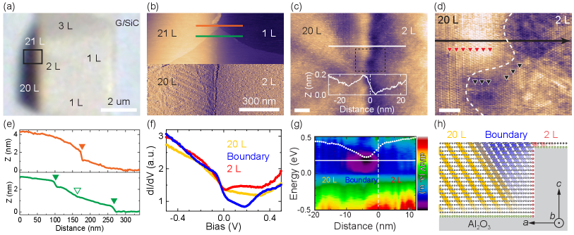
Occasionally, we can find an atomically seamless interface between thin and thick IrTe2 as shown in Figs. 4(a)–(e). Such an interface would provide an unprecedented platform to investigate an interface between 2D and 3D without abrupt steps on the surface. The atom-resolved STM image [Fig. 4(d)] and the height profile [Fig. 4(e)] across the 20/2 L interface clearly demonstrate that the topmost IrTe2 layer is seamlessly connected between 20 L and 2 L while the 21/1 L interface shows an 1-nm-high atomic step. As discussed above, the thicker 21 L and 20 L show the charge orders while the thinner 1 L and 2 L do not [Fig. 4(b)]. In addition, the atom-resolved STM image shows an unambiguous charge order with period of near the interface as indicated by triangles in Fig. 4(d), which is somewhat different from the ground states in bulk showing the charge order Oh et al. (2013); Dai et al. (2014); Chen et al. (2017).
To understand the electronic property of the intriguing interface, the spatially resolved STS measurement is taken across the interface along a black arrow in Fig. 4(d), which exhibits an apparent DOS suppression near = 0.175 V mainly on the 20 L area with width of 10 nm from the interface [Fig. 4(g)]. Such a state near the interface can be qualitatively explained by the strong interlayer coupling. As illustrated in Fig. 4(h), the interlayer coupling delivers electronic properties of edge-terminating atoms (indicated by red circles) to the topmost layer by inducing an exotic DOS suppression only on the 20 L side. On the other hand, the 2 L side does not exhibit such a DOS suppression because its top layer is not connected to any edge-terminating atoms. This finding suggests that the strong interlayer coupling in IrTe2 also plays a vital role in an atomically seamless interface with abrupt thickness changes.
Lastly, the observation of the () charge orders locally near the 2 L region [Fig. 4(d)] contrasts to the absence of the stripe charge order in the isolated bilayer IrTe2 [Fig. 2(b)]. It can be considered as a proximity effect due to the neighboring 20 L. Remarkably, the signatures of the charge order are found nearly nm apart from the interface. The long-range proximity effect in the metallic system is quite unusual, which may indicate the inherent instabilities of IrTe2 against various stripe charge orders. Particularly, the type and stability of the stripe charge order is found to be extremely sensitive to the strain of just % Nicholson et al. (2021). A possible strain near the interface can stabilize the stripe charge ordering phase in the otherwise disorder-induced pristine phase. Therefore, this finding highlights the incipient instability of IrTe2 to charge ordering, which would provide an unprecedented way to create exotic charge-ordered phases by introducing local strains or terminating atomic edges with functional molecules Zhao et al. (2018).
IV Conclusion
We have fabricated the atomically thin and clean IrTe2 flakes varying from monolayer to multilayer by utilizing the Al2O3-assisted exfoliation method, which can overcome the strong coupling between Te interlayers. Our STM/STS measurements exhibit the gradual evolution of charge orders and the exponentially decaying Coulomb gaps with increasing thickness. Our finding reveals that these phenomena are originated from the interplay between the stripe charge ordering with strong interlayer coupling and the substrate-driven disorder. Furthermore, the induced DOS suppression from edge-terminating atoms is found at the atomically seamless interface via the strong interlayer coupling. Our observation strongly suggests that thinner IrTe2 layers would have relatively much lower transition temperature of the charge ordering than our measurement temperature. Further experiments are needed to determine the thickness dependence of the transition temperature.
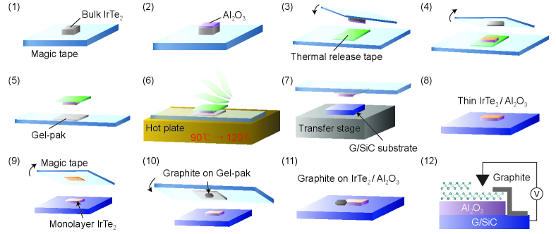
Appendix A Sample Fabrication
To obtain atomically thin IrTe2 flakes, we employ the Al2O3-assisted fabrication method Deng et al. (2018) as shown in Fig. 5. Contrary to the conventional tape exfoliation method Park et al. (2021), this method can produce atomically thin few-layer IrTe2 down to monolayer. For STM measurements, we need to use a piece of exfoliated graphite to bypass insulating Al2O3 between thin IrTe2 flakes and a conducting substrate [see (12) in Fig. 5]. All the fabrication processes should be conducted in an Ar-filled glove box, which prevents any unwanted oxidation or contamination due to oxygen or water. Finally, atomically thin IrTe2 flakes are transferred to an ultra-high vacuum STM chamber without any exposure to air through a home-built suitcase Park et al. (2021).
Appendix B Thickness Determination
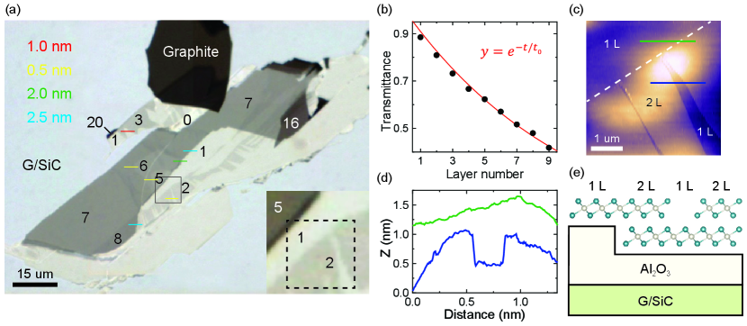
To determine the layer number of IrTe2, we analyze optical transmittance of IrTe2 layers according to the Beer-Lambert law Zhang et al. (2017); Niu et al. (2018). As shown in Fig. 6(b), the quantized transmittance monotonically decreases with increasing layer number. To assign layer numbers unambiguously, STM height measurements are required as demonstrated in Figs. 6(c)–(e). For example, we expect a single atomic step at the 1/2 L interface marked by a dashed line from the OM transmittance contrast [inset of Fig. 6(a)]. However, the corresponding STM image [Fig. 6(c)] does not show any atomic step on the top surface, which means that the expected atomic step exists on the bottom side. In this way, we unambiguously assign thicknesses of IrTe2 flakes as shown in Fig. 6(e).
Acknowledgements.
This work was supported by the National Research Foundation of Korea (NRF) funded by the Ministry of Science and ICT, South Korea (Grants No. NRF-2021R1F1A1063263, 2021R1A6A1A10042944, 2022R1C1C2006027, and 2022M3H4A1A04074153). SYK and JSK was supported by the Institute for Basic Science (IBS) through the Center for Artificial Low Dimensional Electronic Systems (no. IBS-R014-D1). J.K. acknowledges the support from the NRF of Korea grants (NRF-2020R1A2C2103166). SWC is funded in part by the center for Quantum Materials Synthesis (cQMS), funded by the Gordon and Betty Moore Foundation’s EPiQS initiative through grant GBMF10104, and by Rutgers University.References
- Xi et al. (2016) X. Xi, Z. Wang, W. Zhao, J.-H. Park, K. T. Law, H. Berger, L. Forró, J. Shan, and K. F. Mak, Nat. Phys. 12, 139 (2016).
- Song et al. (2021) Y. Song, T. Ying, X. Chen, X. Han, X. Wu, A. P. Schnyder, Y. Huang, J. G. Guo, and X. Chen, Phys. Rev. Lett. 127, 237001 (2021).
- Xi et al. (2015) X. Xi, L. Zhao, Z. Wang, H. Berger, L. Forró, J. Shan, and K. F. Mak, Nat. Nanotechnol. 10, 765 (2015).
- Yu et al. (2015) Y. Yu, F. Yang, X. F. Lu, Y. J. Yan, Y.-H. Cho, L. Ma, X. Niu, S. Kim, Y.-W. Son, D. Feng, S. Li, S.-W. Cheong, X. H. Chen, and Y. Zhang, Nat. Nanotechnol. 10, 270 (2015).
- Chen et al. (2022) P. Chen, Y. H. Chan, R. Y. Liu, H. T. Zhang, Q. Gao, A. V. Fedorov, M. Y. Chou, and T. C. Chiang, Phys. Rev. B 105, L161404 (2022).
- Lin et al. (2017) J. Lin, S. Zuluaga, P. Yu, Z. Liu, S. T. Pantelides, and K. Suenaga, Phys. Rev. Lett. 119, 016101 (2017).
- Ni et al. (2021) Z. Ni, H. Zhang, D. A. Hopper, A. V. Haglund, N. Huang, D. Jariwala, L. C. Bassett, D. G. Mandrus, E. J. Mele, C. L. Kane, and L. Wu, Phys. Rev. Lett. 127, 187201 (2021).
- Ghosh et al. (2010) S. Ghosh, W. Bao, D. L. Nika, S. Subrina, E. P. Pokatilov, C. N. Lau, and A. A. Balandin, Nat. Mater. 9, 555 (2010).
- Jin et al. (2013) W. Jin, P. C. Yeh, N. Zaki, D. Zhang, J. T. Sadowski, A. Al-Mahboob, A. M. Van Der Zande, D. A. Chenet, J. I. Dadap, I. P. Herman, P. Sutter, J. Hone, and R. M. Osgood, Phys. Rev. Lett. 111, 106801 (2013).
- Yang et al. (2012) J. J. Yang, Y. J. Choi, Y. S. Oh, A. Hogan, Y. Horibe, K. Kim, B. I. Min, and S.-W. Cheong, Phys. Rev. Lett. 108, 116402 (2012).
- Yang et al. (2014) J. Yang, W. Wang, Y. Liu, H. Du, W. Ning, G. Zheng, C. Jin, Y. Han, N. Wang, Z. Yang, M. Tian, and Y. Zhang, Appl. Phys. Lett. 105, 063109 (2014).
- Lee et al. (2019) S. H. Lee, J. S. Goh, and D. Cho, Phys. Rev. Lett. 122, 106404 (2019).
- Lee et al. (2021) J. Lee, K. H. Jin, and H. W. Yeom, Phys. Rev. Lett. 126, 196405 (2021).
- Matsumoto et al. (1999) N. Matsumoto, K. Taniguchi, R. Endoh, H. Takano, and S. Nagata, J. Low Temp. Phys. 117, 1129 (1999).
- Machida et al. (2013) T. Machida, Y. Fujisawa, K. Igarashi, A. Kaneko, S. Ooi, T. Mochiku, M. Tachiki, K. Komori, K. Hirata, and H. Sakata, Phys. Rev. B 88, 245125 (2013).
- Joseph et al. (2013) B. Joseph, M. Bendele, L. Simonelli, L. Maugeri, S. Pyon, K. Kudo, M. Nohara, T. Mizokawa, and N. L. Saini, Phys. Rev. B 88, 224109 (2013).
- Dai et al. (2014) J. Dai, K. Haule, J. J. Yang, Y. S. Oh, S.-W. Cheong, and W. Wu, Phys. Rev. B 90, 235121 (2014).
- Hsu et al. (2013) P.-J. Hsu, T. Mauerer, M. Vogt, J. J. Yang, Y. S. Oh, S.-W. Cheong, M. Bode, and W. Wu, Phys. Rev. Lett. 111, 266401 (2013).
- Pascut et al. (2014) G. L. Pascut, K. Haule, M. J. Gutmann, S. A. Barnett, A. Bombardi, S. Artyukhin, T. Birol, D. Vanderbilt, J. J. Yang, S.-W. Cheong, and V. Kiryukhin, Phys. Rev. Lett. 112, 086402 (2014).
- Pyon et al. (2012) S. Pyon, K. Kudo, and M. Nohara, J. Phys. Soc. Japan 81, 053701 (2012).
- Ootsuki et al. (2012) D. Ootsuki, Y. Wakisaka, S. Pyon, K. Kudo, M. Nohara, M. Arita, H. Anzai, H. Namatame, M. Taniguchi, N. L. Saini, and T. Mizokawa, Phys. Rev. B 86, 014519 (2012).
- Kamitani et al. (2013) M. Kamitani, M. S. Bahramy, R. Arita, S. Seki, T. Arima, Y. Tokura, and S. Ishiwata, Phys. Rev. B 87, 180501 (2013).
- Kim et al. (2016) H. S. Kim, S. Kim, K. Kim, B. I. Min, Y.-H. Cho, L. Wang, S.-W. Cheong, and H. W. Yeom, Nano Lett. 16, 4260 (2016).
- Oike et al. (2018) H. Oike, M. Kamitani, Y. Tokura, and F. Kagawa, Sci. Adv. 4, eaau3489 (2018).
- Park et al. (2021) S. Park, S. Y. Kim, H. K. Kim, M. J. Kim, T. Kim, H. Kim, G. S. Choi, C. J. Won, S. Kim, K. Kim, E. F. Talantsev, K. Watanabe, T. Taniguchi, S.-W. Cheong, B. J. Kim, H. W. Yeom, J. Kim, T.-H. Kim, and J. S. Kim, Nat. Commun. 12, 3157 (2021).
- Deng et al. (2018) Y. Deng, Y. Yu, Y. Song, J. Zhang, N. Z. Wang, Z. Sun, Y. Yi, Y. Z. Wu, S. Wu, J. Zhu, J. Wang, X. H. Chen, and Y. Zhang, Nature 563, 94 (2018).
- Hwang et al. (2022) J. Hwang, K. Kim, C. Zhang, T. Zhu, C. Herbig, S. Kim, B. Kim, Y. Zhong, M. Salah, M. M. El-Desoky, C. Hwang, Z. X. Shen, M. F. Crommie, and S. K. Mo, Nat. Commun. 13, 906 (2022).
- Pásztor et al. (2017) Á. Pásztor, A. Scarfato, C. Barreteau, E. Giannini, and C. Renner, 2D Mater. 4, 041005 (2017).
- Efros and Shklovskii (1975) A. L. Efros and B. I. Shklovskii, J. Phys. C Solid State Phys. 8, L49 (1975).
- Lui et al. (2009) C. H. Lui, L. Liu, K. F. Mak, G. W. Flynn, and T. F. Heinz, Nature 462, 339 (2009).
- Lee et al. (2009) N. J. Lee, J. W. Yoo, Y. J. Choi, C. J. Kang, D. Y. Jeon, D. C. Kim, S. Seo, and H. J. Chung, Appl. Phys. Lett. 95, 222107 (2009).
- Li et al. (2013) Y. Li, C.-Y. Xu, and L. Zhen, Appl. Phys. Lett. 102, 143110 (2013).
- Efros (1976) A. L. Efros, J. Phys. C Solid State Phys. 9, 2021 (1976).
- Lauhon and Ho (2001) L. Lauhon and W. Ho, Review of Scientific Instruments 72, 216 (2001).
- Lee et al. (2016) H. Lee, H. O. Jeschke, and R. Valentí, Phys. Rev. B 93, 224203 (2016).
- Szabo et al. (2020) J. C. Szabo, K. Lee, V. Madhavan, and N. Trivedi, Phys. Rev. Lett. 124, 137402 (2020).
- Oh et al. (2013) Y. S. Oh, J. J. Yang, Y. Horibe, and S.-W. Cheong, Phys. Rev. Lett. 110, 127209 (2013).
- Chen et al. (2017) C. Chen, J. Kim, Y. Yang, G. Cao, R. Jin, and E. W. Plummer, Phys. Rev. B 95, 094118 (2017).
- Nicholson et al. (2021) C. W. Nicholson, M. Rumo, A. Pulkkinen, G. Kremer, B. Salzmann, M. L. Mottas, B. Hildebrand, T. Jaouen, T. K. Kim, S. Mukherjee, K. Y. Ma, M. Muntwiler, F. O. von Rohr, C. Cacho, and C. Monney, Commun. Mater. 2, 25 (2021).
- Zhao et al. (2018) X. Zhao, D. Fu, Z. Ding, Y. Y. Zhang, D. Wan, S. J. Tan, Z. Chen, K. Leng, J. Dan, W. Fu, D. Geng, P. Song, Y. Du, T. Venkatesan, S. T. Pantelides, S. J. Pennycook, W. Zhou, and K. P. Loh, Nano Lett. 18, 482 (2018).
- Zhang et al. (2017) H. Zhang, F. Ran, X. Shi, X. Fang, S. Wu, Y. Liu, X. Zheng, P. Yang, Y. Liu, L. Wang, X. Huang, H. Li, and W. Huang, Nanotechnology 28, 164001 (2017).
- Niu et al. (2018) Y. Niu, S. Gonzalez-Abad, R. Frisenda, P. Marauhn, M. Drüppel, P. Gant, R. Schmidt, N. Taghavi, D. Barcons, A. Molina-Mendoza, S. de Vasconcellos, R. Bratschitsch, D. Perez De Lara, M. Rohlfing, and A. Castellanos-Gomez, Nanomaterials 8, 725 (2018).