Dopant size effect on BiFeO3 perovskite structure for enhanced photovoltaic activity
Abstract
This study is carried out using first principles density functional theory calculations within gpaw code. Atomic size effect is analyzed and investigated by doping either Li, Cs or both on Barium doped BiFeO3 (BFO) which belongs to monoclinic space group. The calculated results reveal that Cs doped BFO had significantly improved photocurrent density seemingly due to broadened absorption peaks biplasmons generation. Co-doping two atoms with large size difference have a significant effect on plasmon width peak than doping with a single small sized atom. At higher photon energy realms of the order 10 eV, the index of refraction reduces to implying that light wave can tunnel through the pristine doped BFO without any phase change, thus indicating its potential as an efficient candidate for a photonic application. In addition, doped BFO shows abundant photocurrent generation properties which would be important in solar cell photovoltaic applications.
keywords:
Bismuth ferrite, Density functional theory, Photoelectron, Photovoltaic, Multiferroic, Optical band gap.1 Introduction
BiFeO3 (BFO) is multiferroic perovskite crystal structure, which permits coexistence of varies orders at room temperature. Doping fine or large sized atoms further improves simultaneous coexistence of different orders in single phase resulting in enhanced structural, optical and electronic properties of materials [1].
Several attempts have been done in advancement of the ferromagnetic properties of BFO for improvements in leakage current amount decrement by doping either in A-site or B-site or both sites [2]. Shaan Ameer et al [3] reported that doping Li on BFO reduces ferromagentism. However, optical property enhanced due to small optical band gap energy. Moreover, Aungkan Sen et al [4] suggested proportional doping of Ba Mo in BFO result in improved optical absorbance and dielectric property.
Highest level of doping not only alter the properties of the materials, but had remarkable impact on the crystal structure as well. For instance, La-doped BFO structure is transformed from rhombohedral to triclinic or orthorhombic around 10 mol , and a smaller ionic radius rare-earth doping at the B-site causes structural distortion, and brought forth antiferroelectric-like double-hysteresis P-E loops. Moreover, rare-earth elements with a smaller ion radius, because of a geometrical magnetic moments factor, are forced to align themselves either in symmetrical or antisymmetrical orientation, resulting in various magnetic order phases. Arnold et al [5] also ascertained that rare-earth doped BFO materials’ ionic radii at B-site are the prominent source for phase transitions and structural phase transitions, which is also supported by other literatures [6, 7, 8].
Besides phase, structural and property alteration, chemical strain forces can be exhibited among atoms because of short and long range interactions. J.A. Schiemer et al [9] studied significance of strain in coupling phase orders with effect on elastic response of either in high or low level doped crystals in relation to magnetic order, oxygen vacancy dynamics, and conductivity. It is also inferred that important transformation in multiferroic properties are highly correlated to structural changes. It has been well understood that applied strain on BFO scales up the magnetic, piezoelectric, ferroelectric, and optical properties [10].
Liang Bai et al [11] also experimented and observed that doping Co3+ ions knocks out Fe3+ ions from B-sites and opens up for random substitute. Consequently, a spirally arranged spin becomes disrupted and chemical strain is grown because of uneven size of the two B-site cations (Co3+ and Fe3+ ions)). In spite of the previous efforts, strain evolution due to dopant size its facilitation for coupling of multiferroic orders still remains debatable. Here we considered perovskite monoclinic BFO () phase the experimentally synthesized counterpart as heated over a range of high temperature during sintering processes, is evidenced with appearance of several phases plus parasitic phase (Bi2Fe4O9) [12].
In the course of sintering process, various transformation is undergone as function of temperature leading to bismuth depreciated, due to its volatility resulting in impure BFO phases, which is often called secondary phase of the cubic structure. However, these phases are further purified by proportional addition of Bi2O3 and Fe2O3 [13], see Eq. (1).
| (1) |
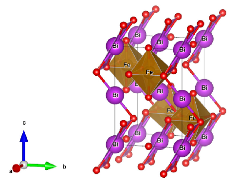
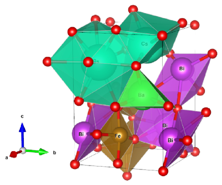
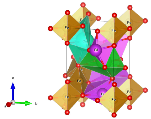
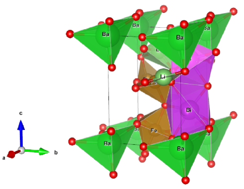
We considered perovskite monoclinic BFO () phase because one could easily understand doping effect. Therefore, this work explores cesium (Cs) and lithium (Li) size effect on barium (Ba) doped BiFeO3. It results in structural phase transition due to strain created because of size of substitute atoms (Fig. 1).
2 Computational method
Ab initio calculations were performed using the projector augmented wave (PAW) method as implemented in gpaw code [14]. The electron wave-function is approximated using the implementation of a projector augmented wave method [15] the Schrdinger equation applied to total energy functions are solved self-consistently using the Kohn-Sham scheme [16]. All electron waves are expanded over periodic potential plane with a method of P.E. Blchl [17] having a band, a k-points, and a reciprocal lattice grid indices. A plane wave cut-off energy used is 520 eV. The k-points within Brillouin zone (BZ) is chosen according to Monkhorst-Pack scheme [18], where a -mesh of 888 is used.
The interactions of the valence electrons with the core electrons and nuclei is treated within a projector augmented wave (paw) data sets [14, 15]. The number of valence electrons considered for each element within the paw data sets is Bi (5d106s26p3), Fe (3d64s2), O (2s22p4), Cs (5s25p66s1), Li (2s1), Ba (5s25p66s2), Geometry relaxations are carried out using BFGS minimizer [19], where optimizations of the atomic coordinates and the unit cell degrees of freedom is done within the concept of the Hellmann-Feynman forces and stresses [20, 21] calculated on the Born-Oppenheimer (BO) surface [22]. The convergence criteria for the forces were set at 0.05 . The exchange-correlation energies are approximated within the generalized gradient approximation of PBE [23] a -mesh of 888 is used in a geometry relaxation calculations. The strongly correlated nature of electrons of Fe were treated using Hubbard-like model which is introduced into the Gpaw code according to [24, 25], where U-J=7.5 eV.
Brillouin zone integration were performed with the tetrahedron method which is proved efficient especially for excited states magnetically induced dielectric function calculation [26]. Ground state calculation is performed with k-point density of 5 points per with -point inclusion. A restarted calculations were done with a fixed density of 7.5 points per over densely sampled k-points grid. The k-point density is calculated as:
| (2) |
where N is the number of k-points and is the reciprocal of a lattice vector of the unit-cell. One can analyse and understand material’s optical response property once incident photon energy is imparted to the electron, where the material’s response or dielectric function is given as
| (3) |
The imaginary part is calculated from the density matrix of the electronic structure [27] according to the implementations by the group of G. Kresse [28, 29], given by
| (4) |
where is the electronic charge, and and are the conduction band (CB) and valence band (VB) wave functions at k, respectively, is the energy of the incident phonon, is the momentum operator, is a joint density of states, is volume of the primitive cell.
The Real part of the dielectric function can be found from the Kramer-Kronig equation [30].
| (5) |
where, P stands for the principal value of the integral. The optical absorption coefficient was obtained by using Eq. (6)
| (6) |
where is photon frequency, is speed of light. are frequency dependent real and imaginary parts of dielectric function as stated in Eq. (3). For photovoltaic applications, the BFO should be able to absorb as much light as possible to generate a photocurrent, which requires a lower band gap and a large absorption coefficient.
The photocurrent density under irradiation with a certain wavelength can be described by an empirical Glass Law [31].
| (7) |
where is the optical absorption coefficient, is a material-dependent Glass coefficient, and I is irradiation intensity. The photocurrent density is linearly proportional to the absorption coefficient. The relation between and an optical band gap can be estimated using the Tauc relation [32].
| (8) |
where A is a material dependent constant and is the incident photon energy. According to Eq. (7) Eq. (8), one can extrapolate a larger photocurrent density by increasing the absorption coefficient with a small band gap.
From dielectric function, all the other optical properties such as, reflectivity , refractive index , extinction coefficient is also obtained [33, 34, 35], given as follows.
| (9) |
In addition, reflectivity , energy loss function is calculated as
| (10) |
and
| (11) |
respectively.
The spin-orbit module calculates spin-orbit band structures non-self consistently. The input is a standard converged GPAW calculation and the module diagonalizes the spin-orbit Hamiltonian in a basis of scalar-relativistic Kohn-Sham eigenstates. Since the spin-obit coupling is largest close to the nuclei, we only consider contributions from inside the PAW augmentation spheres where the all-electron states can be expanded as
| (12) |
The full Bloch Hamiltonian in a basis of scalar relativistic states becomes
| (13) |
where the spinors are chosen along the z-axis as default. It is also possible to obtain the eigenstates of the full spin-orbit Hamiltonian as well as the spin character along the z-axis. The spin character is defined as
| (14) |
and is useful for analysing the degree of spin-orbit induced hybridization between spin up and spin down states [36].
3 Results and Discussion
Experimental refined x-ray diffraction structural positions were obtained from Inorganic Crystal Structure Database (ICSD) [37]. Structural volume optimization made over lattice range 5.0 to 6.0 , and obtained , , , and , , which are in close agreement to experimental parameters. The bulk modulus at monoclinic space group (Fig. 1) is found to be , also shown weak ferromagnetism with average a remnant magnetization of 3.510-6 /Fe. This value is close to literature value 410-6 /Fe [38].
Band structure is calculated in Fig. 2 using spin-orbit coupling module as implemented in the Gpaw electronic structure code, plotted over special k-points which were exported online according to a literature [39] by inputting the crystallographic information file of space group.
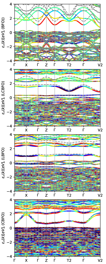
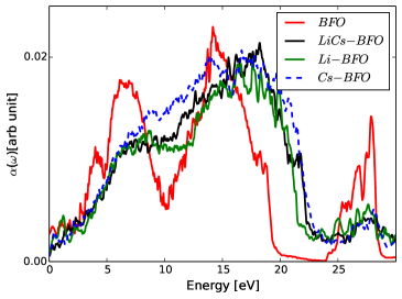
The calculated absorption coefficient of pristine compared with doped bismuth ferrite are shown in Fig. 3. The absorption ability seems to be reduced for all doped systems compared to pristine BFO in low energy-loss region. In addition, the optical bandgap is significantly decreased as illustrated in the Table. 1, but a dopant size also seems to have an effect on the optical gap (Fig. 2).
| System | Magnetization [] | Optical band gap [eV] | Moment per Fe-atom [/Fe] |
|---|---|---|---|
| BFO | 1.510-6 | 2.13275 | 410-6 |
| LiCs-BFO | 0.000 | 0.6855 | 0.000 |
| Li-BFO | 210-6 | 0.7125 | 110-6 |
| Cs-BFO | 1.532450 | 0.6746 | 0.71731 |
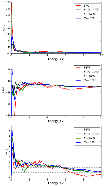
The imaginary part, (Fig. 3) shows absorption peaks in a photon energies range of 0.0-10.0 eV. The imaginary part is associated with only inter-band transition, and the real part approaches to zero at certain realms of photon energies, signaling a resonance at which collective electrons start to excite at plasma frequency.
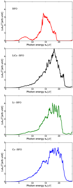
It looks from Fig. 2 that a congested bound of bands near the Fermi level of valence band seems to oscillate with plasma frequency. From Fig. 4, the optical bandgaps presented in the Table 1 are calculated using Tauc relation (Eq. (8)), & according to a tangent line curve fitting approach adopted from a literature [40].
We also notice from Figs. 4 5 that absorption peaks occur over a wider ranges of photon energies by doping the BFO, that a decrease in the imaginary part at higher photon energy potentially indicates a decline in absorption of photon energy to bound electron of valance band. Thus, the excitation of the plasmons by light is demonstrated by a decrease of the reflectivity of the light at plasma frequency because of photon energy is consumed up by oscillating bound electrons. The refractive index as indicated in Fig. 5 show that , at high photon energies ( 10-15 eV). This could potentially imply that light can pass through the material without a phase change, which is a novel characteristics of photonic crystals. Such a claim also agrees with experimental theoretical concepts explained in literature [41, 42].
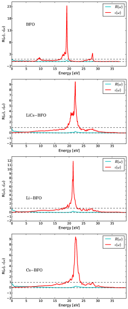
As shown in Fig. 6, plasmons move in a periodic potential and unlike ideal plasmons, and pristine BFO, had three peaks at 10 eV, 19 eV 27 eV. Li Cs co-doped BFO had three peaks at 21 eV, 24 eV, 27 eV. Li doped BFO had two peaks at 21 eV, 28 eV. Cs doped BFO had three peaks at 15 eV, 26 eV, 28 eV. The energy-loss may show plasmon excitation in region of about 10-30 eV often during inter-band transition of single electron. However, high energy-loss region is highly associated with excitation of bound electron with multiple peaks. These bound electron significantly increase photocurrent generation which enormously enhance photovoltaic effect. It is been noted that two plasmons of pristine BFO interact via electron-hole pair resulting in biplasmons generation due to Cs doping. However, Li doping affected the amount of energy of the two peak points plus a very small peak at 30 eV. Therefore, Cs size had effect on biplasmons generation in comparison to the Li size. In some cases, plasmons width peak explain the phase changes. We can infer that size of the dopant atom has remarkable impact on both number width of plasmons resulting in enhanced photovoltaic property. Hence, co-doping of Li Cs in a Barium doped bismuth ferrite seems to have a potential for improved efficiency as a photoelectron capturing device.
4 Conclusion
The investigations can be summarized as follows.
-
1.
With doping, absorption coefficient has widened resulting to a decreased optical bandgap hence shows a potential for an increased solar cell property.
-
2.
A squared absorption coefficient peak shows an increase in width of by about 4 eV towards a realm of higher photon energies in the case of doped BFO. This is believed to be a sign of an increased solar cell activity.
-
3.
Dielectric functions seem to have large values at zero photon energies, but these values seem to be reduced significantly by an introduction of a series of photon energies of up to =10 eV. For photon energies of 10-15 eV, .
-
4.
The crossing of the imaginary part of the dielectric function of a zero values at multiple realms of the photon energies indicates a potential importance of the system in applications based on photonic conductivity.
-
5.
The systems’ , , seem to be reduced rapidly with introduction of photon energies, while a major contributor to the magnitude of seems to be .
-
6.
Expanded width of energy loss peaks happen with doping an occurrence of such peaks at higher photon energies indicates a potential importance for applications in a plasmonic effect.
Disclosure statement
The authors declare that there is no conflict of interest.
Acknowledgements
We are grateful to the Ministry of Science and Higher Education of Ethiopia for financial support. The authors also acknowledge the Department of Physics at Addis Ababa University and the International Science Program, Uppsala University, Sweden, for providing computer facilities.
ORCID iDs
K.N. Nigussa.
https://orcid.org/0000-0002-0065-4325.
References
-
[1]
C.-H. Yang, D. Kan, I. Takeuchi, V. Nagarajan, J. Seidel,
High temperature phase
transitions in tungsten trioxide-the last word?, J. Phys. Condensed Matter
13 (2001) 1.
URL https://doi.org/10.1088/0953-8984/14/3/308 -
[2]
Q. Yang, Q. Xu, M. Sobhan, Q. Ke, F. Anariba, K. Ong, P. Wu,
Simultaneous reduction in
leakage current and enhancement in magnetic moment in BiFeO3
nanofibers via optimized Sn doping, physica status solidi (RRL)-Rapid
Research Letters 8 (7) (2014) 653–657.
URL https://doi.org/10.1002/pssr.201409043 -
[3]
S. Ameer, K. Jindal, M. Tomar, P. Jha, V. Gupta,
Effect of Li doping on
the electronic and magnetic properties of BiFeO3 by first
principles, Integrated Ferroelectrics 193 (1) (2018) 123–128.
URL https://doi.org/10.1080/10584587.2018.1514875 -
[4]
A. Sen, M. Hasan, Z. Islam, M. Hassan, T. Zaman, M. Matin, F. Gulshan,
Influence of Ba and Mo
co-doping on the structural, electrical, magnetic and optical properties of
BiFeO3 ceramics, Materials Research Express 7 (1) (2020)
016312.
URL https://doi.org/10.1088/2053-1591/ab6801 -
[5]
D. Arnold, Composition-driven
structural phase transitions in rare-earth-doped BiFeO3
ceramics: a review, IEEE Transactions on Ultrasonics, Ferroelectrics, and
Frequency Control 62 (1) (2015) 62–82.
URL https://doi.org/10.1109/TUFFC.2014.006668 -
[6]
H. Tao, J. Lv, R. Zhang, R. Xiang, J. Wu,
Lead-free rare
earth-modified BiFeO3 ceramics: Phase structure and electrical
properties, Materials and Design 120 (2017) 83–89.
URL https://doi.org/10.1016/j.matdes.2017.01.083 - [7] K. Nalwa, A. Garg, Phase evolution, magnetic and electrical properties in Sm-doped bismuth ferrite, Journal of Applied Physics 103 (4) (2008) 044101.
-
[8]
D. Kan, L. Palova, V. Anbusathaiah, C. Cheng, S. Fujino, V. Nagarajan, K. Rabe,
I. Takeuchi, Universal behavior
and electric-field-induced structural transition in rare-earth-substituted
BiFeO3, Advanced Functional Materials 20 (7) (2010)
1108–1115.
URL https://doi.org/10.1002/adfm.200902017 -
[9]
J. Schiemer, R. Withers, Y. Liu, M. Carpenter,
Ca-doping of BiFeO3:
The role of strain in determining coupling between ferroelectric
displacements, magnetic moments, octahedral tilting, and oxygen-vacancy
ordering, Chemistry of Materials 25 (21) (2013) 4436–4446.
URL https://doi.org/10.1021/cm402962q -
[10]
H. Hojo, K. Onuma, Y. Ikuhara, M. Azuma,
Structural evolution and
enhanced piezoresponse in cobalt-substituted BiFeO3 thin
films, Applied Physics Express 7 (9) (2014) 091501.
URL https://doi.org/10.7567/apex.7.091501 -
[11]
L. Bai, M. Sun, W. Ma, J. Yang, J. Zhang, Y. Liu,
Enhanced magnetic properties of
Co-doped BiFeO3 thin films via structural progression,
Nanomaterials 10 (9).
URL https://doi.org/10.3390/nano10091798 -
[12]
R. Haumont, I. Kornev, S. Lisenkov, L. Bellaiche, J. Kreisel, B. Dkhil,
Phase stability and
structural temperature dependence in powdered multiferroic
BiFeO3, Phys. Rev. B 78 (2008) 134108.
URL https://doi.org/10.1103/PhysRevB.78.134108 - [13] U. Nuraini, S. Suasmoro, Crystal structure and phase transformation of BiFeO3 multiferroics on the temperature variation, Journal of Physics: Conference Series.
-
[14]
J. Enkovaara, C. Rostgaard, J. Mortensen, J. Chen, M. Dułak, L. Ferrighi,
J. Gavnholt, C. Glinsvad, V. Haikola, H. Hansen, H. Kristoffersen, M. Kuisma,
A. Larsen, L. Lehtovaara, M. Ljungberg, O. Lopez-Acevedo, P. Moses,
J. Ojanen, T. Olsen, V. Petzold, N. Romero, J. Stausholm-Mller,
M. Strange, G. Tritsaris, M. Vanin, M. Walter, B. Hammer,
H. Hkkinen, G. Madsen, R. Nieminen, J. Nrskov,
M. Puska, T. Rantala, J. Schitz, K. Thygesen, K. Jacobsen,
Electronic structure
calculations with GPAW: a real-space implementation of the projector
augmented-wave method, J. Phys.: Condens. Matter 22 (2010) 253202.
URL https://doi.org/10.1088/0953-8984/22/25/253202 -
[15]
J. Mortensen, L. Hansen, K. Jacobsen,
Real-space grid
implementation of the projector augmented wave method, Phys. Rev. B 71
(2005) 035109.
URL https://doi.org/10.1103/PhysRevB.71.035109 -
[16]
W. Kohn, L. Sham,
Self-consistent equations
including exchange and correlation effects, Phys. Rev. 140 (1965)
A1133–A1138.
URL https://doi.org/10.1103/PhysRev.140.A1133 -
[17]
P. Blchl,
Projector augmented-wave
method, Phys. Rev. B 50 (1994) 17953.
URL https://doi.org/10.1103/PhysRevB.50.17953 -
[18]
H. Monkhorst, J. Pack, Special
points for Brillouin-zone integrations, Phys. Rev. B 13 (1976) 5188.
URL https://doi.org/10.1103/PhysRevB.13.5188 -
[19]
H. Schlegel, Optimization of
equilibrium geometries and transition structures, J. Comp. Chem. 3 (1982)
214.
URL https://doi.org/10.1002/jcc.540030212 -
[20]
P. Feynman, Forces in
Molecules, Phys. Rev. 56 (1939) 340.
URL https://doi.org/10.1103/PhysRev.56.340 -
[21]
O. Nielsen, R. Martin,
Quantum-mechanical theory of
stress and force, Phys. Rev. B. 32 (1985) 3780.
URL https://doi.org/10.1103/PhysRevB.32.3780 -
[22]
R. Wentzcovitch, J. Martins,
First principles
molecular dynamics of Li: Test of a new algorithm, Solid State Commun.
78 (1991) 831.
URL https://doi.org/10.1016/0038-1098(91)90629-A -
[23]
J. Perdew, K. Burke, M. Ernzerhof,
Generalized Gradient Approximation Made Simple,
Phys. Rev. Lett. 77 (1996) 3865.
URL https://doi.org/10.1103/PhysRevLett.77.3865 -
[24]
A. Liechtenstein, V. Anisimov, J. Zaane,
Density-functional theory
and strong interactions: orbital ordering in mott-hubbard insulators,
Phys. Rev. B 52 (1995) R5467.
URL http://dx.doi.org/10.1103/PhysRevB.52.R5467 -
[25]
S. Dudarev, G. Botton, S. Savrasov, C. Humphreys, A. Sutton,
Electron-energy-loss spectra
and the structural stability of nickel oxide: an LSDA+U study,
Phys. Rev. B 57 (1998) 1505.
URL http://dx.doi.org/10.1103/PhysRevB.57.1505 -
[26]
A. MacDonald, S. Vosko, P. Coleridge,
Extensions of the
tetrahedron method for evaluating spectral properties of solids, Journal of
Physics C: Solid State Physics 12 (15) (1979) 2991–3002.
URL https://doi.org/10.1088/0022-3719/12/15/008 -
[27]
M. Hybertsen, S. Louie, Ab
initio static dielectric matrices from the density-functional approach:
Formulation and application to semiconductors and insulators, Phys. Rev. B 35 (1987) 5585.
URL https://doi.org/10.1103/PhysRevB.35.5585 -
[28]
M. Gajdo, K. Hummer, G. Kresse, J. Furthmller,
F. Bechstedt, Linear
optical properties in the projector-augmented wave methodology, Phys. Rev. B 73 (2006) 045112.
URL https://doi.org/10.1103/PhysRevB.73.045112 -
[29]
M. Shishkin, G. Kresse,
Implementation and
performance of the frequency-dependent GW method within the PAW
framework, Phys. Rev. B 74 (2006) 035101.
URL https://doi.org/10.1103/PhysRevB.74.035101 - [30] F. Wooten, Optical Properties of Solids, Academic Press, New York, 1972.
-
[31]
A. Glass, D. v. Linde, T. Negran,
High‐voltage bulk photovoltaic
effect and the photorefractive process in LiNbO3, Applied
Physics Letters 25 (4) (1974) 233–235.
URL https://doi.org/10.1063/1.1655453 -
[32]
J. Tauc, R. Grigorovici, A. Vancu,
Optical properties and
electronic structure of amorphous germanium, physica status solidi (b)
15 (2) (1966) 627–637.
URL https://doi.org/10.1002/pssb.19660150224 -
[33]
T. Ada, K. Nigussa, L. Deja,
The effect of
non-centrosymmetricity on optical and electronic properties of
BaHfO3 perovskite, Computational Condensed Matter 26 (2021)
e00524.
URL https://doi.org/10.1016/j.cocom.2020.e00524 -
[34]
T. Shen, C. Hu, H. Dai, W. Yang, H. Liu, X. Wei,
First principles
study of structural, electronic and optical properties of
BiFeO3 in ferroelectric and paraelectric phases, Materials
Research Innovations 19 (sup5) (2015) S5–684–S5–688.
URL https://doi.org/10.1179/1432891714Z.0000000001176 -
[35]
Z. Teng, J. Jiang, G. Chen, C. Ma, F. Zhang,
The electronic structures and
optical properties of B, C or N doped BaTiO3, AIP
Advances 8 (9) (2018) 095216.
URL https://doi.org/10.1063/1.5047094 -
[36]
T. Olsen, Designing in-plane
heterostructures of quantum spin hall insulators from first principles:
with
adsorbates, Phys. Rev. B 94 (2016) 235106.
URL https://doi.org/10.1103/PhysRevB.94.235106 -
[37]
P. Paufler, International
tables for crystallography, Acta Cryst. A63 (2007) 483.
URL https://doi.org/10.1107/S0108767307041207 -
[38]
S. Zhang, M. Lu, D. Wu, Y. Chen, N. Ming,
Larger polarization and weak
ferromagnetism in quenched BiFeO3 ceramics with a distorted rhombohedral crystal structure, Applied Physics Letters 87 (2005) 26.
URL https://doi.org/10.1063/1.2147719 -
[39]
Y. Hinuma, G. Pizzi, Y. Kumagai, F. Oba, I. Tanaka,
Band structure diagram
paths based on crystallography, Comp. Mat. Sci. 128 (2017) 140.
URL https://doi.org/10.1016/j.commatsci.2016.10.015 -
[40]
Y.-T. Peng, S.-H. Chiou, C.-H. Hsiao, C. Ouyang, C.-S. Tu,
Remarkably enhanced photovoltaic
effects and first-principles calculations in neodymium doped bifeo3,
Scientific Reports 7 (2017) 45104.
URL https://doi.org/10.1038/srep45164 -
[41]
J. Schilling, The quest for
zero refractive index, Nature Photonics 5 (8) (2011) 449–451.
URL https://doi.org/10.1038/nphoton.2011.172 -
[42]
I. Liberal, N. Engheta,
Near-zero refractive index
photonics, Nature Photonics 11 (3) (2017) 149–158.
URL https://doi.org/10.1038/nphoton.2017.13