Enhanced light absorption in Tamm metasurface with a bound state in the continuum
Abstract
We consider light absorption in a germanium grating placed on top of photonic-crystalline substrate. Such a system supports an optical Tamm state decoupled from the continuous spectrum with its frequency within the photonic band gap. We have demonstrated that application of the Tamm state makes in possible to engineer extremely narrow absorber which provides a absorption in a semiconductor grating in the critical coupling regime. The proposed design may be used at both normal and oblique incidence at the telecom wavelength.
Localized modes in periodic structures are of great interest due to record high Q-factors Akahane et al. (2003); Song et al. (2005); Asano et al. (2017) as well as the opportunity to design tunable devices by using liquid crystals Hsiao (2019), nonlinear media SoljaČiĆ and Joannopoulos (2004) or resonant materials Moiseev et al. (2019). Along with studies on volume electromagnetic waves localized in structural defects, attention is paid to surface waves localized at the boundary with negative dielectric permittivity media. In this case, the light is trapped at the boundary between plasmonic and dielectric structures. These localized states are called Tamm plasmon polaritons Kaliteevski et al. (2007) (TPPs). The TPPs are applied for engineering optical devices, such as photoelectrochemical cells Pyatnov et al. (2022), sensors Juneau-Fecteau et al. (2021), lasers Xu et al. (2021), beam steerers Bikbaev et al. (2022) and solar cells Bikbaev et al. (2020). Coupling of TPPs with other types of localized modes, for example, with a surface plasmon-polariton Afinogenov et al. (2013), leads to hybrid modes which are widely applied in optical sensorsDas et al. (2015); Buzavaite-Verteliene et al. (2020). Tailoring the parameters of TPP supporting structures makes it possible to set-up the critical coupling at which all radiation incident on the structure is absorbed at the TPP wavelength. This resonant absorption mechanism is used in absorbers Kim et al. (2022); Bikbaev et al. (2019) and photodetectors Wang et al. (2020a); Zhang et al. (2017). Such surface-localized status can be excited at the boundary between a photonic crystal and plasmonic Buchnev et al. (2020, 2022) or dielectric metasurfaces Bikbaev et al. (2021a). In the latter case, such localized states are called optical Tamm states.
Lately, we have seen a surge of interest to photonic non-radiation states, i.e. optical bound states in the continuum (BICs) Hsu et al. (2016); Koshelev et al. (2019); Sadreev (2021) which have become an important instrument for engineering optical devices with enhanced light-matter interaction. In the presence of material absorption the BIC is shown to acquire finite-life, albeit remain localized and decoupled from the outgoing channels Hu et al. (2020). Quasi-BIC in lossy periodic structures is found to be instrumental for enhancement of light absorption Saadabad et al. (2021); Tan et al. (2022) in the critical coupling regime even in low loss dielectrics. Therefor, BIC concept opens novel opportunities for highly efficient light absorbers Zhang and Zhang (2015); Wang et al. (2020b); Sang et al. (2021); Xiao et al. (2021); Cai et al. (2022).
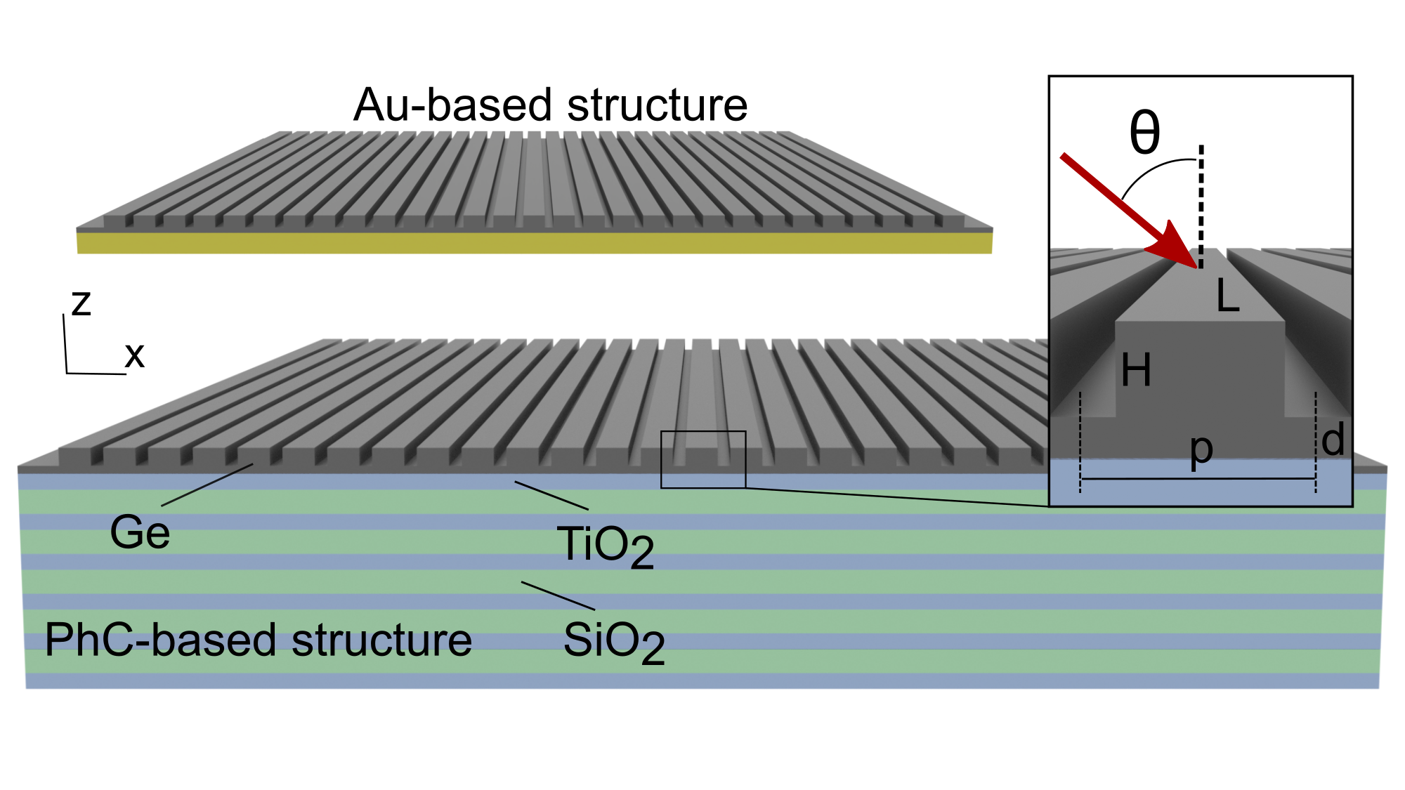
It has been demonstrated in Saadabad et al. (2021) that application of perfect mirror in the substrate of a BIC supporting structures makes it possible to set-up a perfect light absorber in the so-called critical coupling regime when the radiative and non-radiative -factors are equal to one another. In practice the mirror substrate for a dielectric structure can be implemented as an opaque metal film. All metals, however, exhibit significant material losses so the radiation is absorbed not only in the dielectric or semiconductor but in the mirror itself. Thus, the electromagnetic energy is wasted on heating the substrate rather than produce the desirable photoelectric effect. In this letter we propose a set-up with a non-absorbing mirror which leads to of incident radiation absorbed in the germanium (Ge) metasurface Zhou et al. (2022). In Table 1 of paper Odit et al. (2020), the calculated total Q-factor () of Ge is quite high at 1.5m. For designing high-Q metasurfaces at 1.5m, it is more suitable than silicon in group IV. The system is depicted in Fig. 1. The structure consists of a periodic Ge grating placed on top of 1D photonic crystal. Later on the set-up will be referred to as the PhC-based structure. For comparison we will consider a similar Ge grating but placed on an Au substrate. The latter set-up will be referred to as the Au-based structure and is also shown in Fig. 1.
The Tamm metasurface structure has been proposed in our previous work Bikbaev et al. (2021b) where we demonstrated that an off- BIC leads to emergence of critical coupling (CC) points in the parameter space of incident frequency and incident angle . In Bikbaev et al. (2021b) the critical coupling effect occurred as zero reflection due to tunnelling across the band-gap in the PhC substrate with a finite number of bilayers. Here we suppose that the substrate is thick enough to suppress the tunneling and expect that the reflectance zeros are associated with the perfect light absorption.
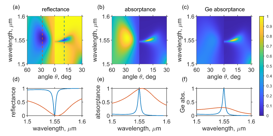
First, let us compare light absorption by the PhC- and Au-based structures. To carry out the comparison we defined the parameters of the structures such that both support an in- BIC at frequency m. Corresponding parameters of the structure are presented in caption of Fig.1. The BICs do not couple with the incident light at the normal incidence. Therefore, to obtain the critical coupling one has to vary the angle of incidence. The increase of the angle of incidence results in a drop of the radiative -factor of the leaky band hosting the BIC until the radiation and material loss rates are equal to one another. This effect is visible in the reflectance spectra of the structures calculated by the finite difference time domain method shown in Fig. 2 (a). In the PhC-based structure the critical coupling is achieved at deg., thereas in the Au-based structure the critical coupling angle is deg. The Au-based structure is more lossy, hence the critical coupling is observed at a larger angle of incidence with a larger width of the resonance. One can see in Fig. 2 (b) that in both structures of incident radiation is absorbed at the critical coupling. However, as seen in Fig. 2 (c) less than 30% of energy is absorbed in Ge in the Au-based structure while in the PhC-based structure the absorptance in Ge is . Such a large difference in the absorption of the Ge is due to the fact that most of the radiation incident on the Au-based structure is absorbed in the plasmonic substrate, while in the PhC-based structure the substrate is all-dielectric. For the reader’s convenience, the frequency dependencies of the absorption and reflection coefficients at the critical coupling are shown in Fig. 2 (d-f).
Notice that with an in- BIC the critical coupling is never obtained at the normal incidence. To engineer the perfect absorption in Ge at the normal incidence we return to an off- BIC reported in Bikbaev et al. (2021b). Following Bikbaev et al. (2021b) we describe the scattering spectrum of the Ge-based structure in the framework of the temporal coupled mode theory Fan et al. (2003) which yields the following solution for the reflection amplitude
| (1) |
where is the frequency of the incident wave, - the resonant frequency, - the angle of incidence, is the loss rate due to coupling to radiation to the upper half-space, and is the loss rate due to absorption. According to Bulgakov and Maksimov (2017) the dispersion of and are given by
| (2) |
where is the angle corresponding to the off- BIC in the spectrum while and are fitting parameters which can be obtained from numerical simulations. The absorption coefficient can be written as
| (3) |
The critical coupling points are topologically protected objects associated with phase singularities of the reflection amplitude Bikbaev et al. (2021b). For this reason, the effects of critical coupling and perfect light absorption survive under variation of the system’s parameters preserving all symmetries of the structure. Thus, by changing the parameters one can achieve the critical coupling in the -point if
| (4) |
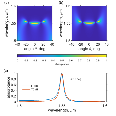
By varying the grating period we achieve the in- critical coupling in the Ge-based structure with period nm which led to the following values of the TCMT parameters m-1deg-2, m-1deg-4, m. In Fig. 3 (a-b) we compare the numerical data against Eq. (3). The absorption spectrum at the normal incidence is shown in Fig. 3 (c). One can see a good coincidence between the full-wave simulations and the TCMT approximation of the spectrum.
In summary, we have demonstrated that application of a high-Q Tamm state makes in possible to engineer a perfect light absorber which provides a absorption in a semiconductor grating. The proposed design may be used at both normal and oblique incidence at the telecom wavelength. We believe that the reported wavelength and angle selectivity can be of use in small LiDAR detectors.
This research was funded by the Russian Science Foundation (project no. 22-42-08003). This work was supported by the Higher Education Sprout Project of the National Yang Ming Chiao Tung University and Ministry of Education and the National Science and Technology Council (NSTC 109-2628-E-007 -003 -MY3; 111-2923-E-007 -008 -MY3; 111-2628-E-007-021 ).
The authors declare no conflicts of interest.
References
- Akahane et al. (2003) Y. Akahane, T. Asano, B.-S. Song, and S. Noda, Nature 425, 944 (2003).
- Song et al. (2005) B.-S. Song, S. Noda, T. Asano, and Y. Akahane, Nature Materials 4, 207 (2005).
- Asano et al. (2017) T. Asano, Y. Ochi, Y. Takahashi, K. Kishimoto, and S. Noda, Optics Express 25, 1769 (2017).
- Hsiao (2019) Y.-C. Hsiao, in Photonic Crystals - A Glimpse of the Current Research Trends (IntechOpen, 2019).
- SoljaČiĆ and Joannopoulos (2004) M. SoljaČiĆ and J. D. Joannopoulos, Nature Materials 3, 211 (2004).
- Moiseev et al. (2019) S. G. Moiseev, I. A. Glukhov, Y. S. Dadoenkova, and F. F. L. Bentivegna, Journal of the Optical Society of America B 36, 1645 (2019).
- Kaliteevski et al. (2007) M. Kaliteevski, I. Iorsh, S. Brand, R. A. Abram, J. M. Chamberlain, A. V. Kavokin, and I. A. Shelykh, Physical Review B 76, 165415 (2007).
- Pyatnov et al. (2022) M. Pyatnov, R. Bikbaev, I. Timofeev, I. Ryzhkov, S. Vetrov, and V. Shabanov, Nanomaterials 12, 928 (2022).
- Juneau-Fecteau et al. (2021) A. Juneau-Fecteau, R. Savin, A. Boucherif, and L. G. Fréchette, AIP Advances 11, 065305 (2021), https://doi.org/10.1063/5.0054629 .
- Xu et al. (2021) W.-H. Xu, Y.-H. Chou, Z.-Y. Yang, Y.-Y. Liu, M.-W. Yu, C.-H. Huang, C.-T. Chang, C.-Y. Huang, T.-C. Lu, T.-R. Lin, and K.-P. Chen, Advanced Photonics Research 3, 2100120 (2021).
- Bikbaev et al. (2022) R. G. Bikbaev, D. N. Maksimov, K.-P. Chen, and I. V. Timofeev, Materials 15, 6014 (2022).
- Bikbaev et al. (2020) R. G. Bikbaev, S. Y. Vetrov, I. V. Timofeev, and V. F. Shabanov, Doklady Physics 65, 161 (2020).
- Afinogenov et al. (2013) B. I. Afinogenov, V. O. Bessonov, A. A. Nikulin, and A. A. Fedyanin, Applied Physics Letters 103, 061112 (2013).
- Das et al. (2015) R. Das, T. Srivastava, and R. Jha, Sensors and Actuators B: Chemical 206, 443 (2015).
- Buzavaite-Verteliene et al. (2020) E. Buzavaite-Verteliene, I. Plikusiene, T. Tolenis, A. Valavicius, J. Anulyte, A. Ramanavicius, and Z. Balevicius, Optics Express 28, 29033 (2020).
- Kim et al. (2022) S. H. Kim, J. H. Ko, Y. J. Yoo, M. S. Kim, G. J. Lee, S. Ishii, and Y. M. Song, Advanced Optical Materials 10, 2102388 (2022).
- Bikbaev et al. (2019) R. Bikbaev, S. Vetrov, and I. Timofeev, Photonics 6, 28 (2019).
- Wang et al. (2020a) J. Wang, Y. Zhu, W. Wang, Y. Li, R. Gao, P. Yu, H. Xu, and Z. Wang, Nanoscale 12, 23945 (2020a).
- Zhang et al. (2017) C. Zhang, K. Wu, V. Giannini, and X. Li, ACS Nano 11, 1719 (2017).
- Buchnev et al. (2020) O. Buchnev, A. Belosludtsev, V. Reshetnyak, D. R. Evans, and V. A. Fedotov, Nanophotonics 9, 897 (2020).
- Buchnev et al. (2022) O. Buchnev, A. Belosludtsev, and V. A. Fedotov, ACS Applied Materials Interfaces 14, 13638 (2022).
- Bikbaev et al. (2021a) R. G. Bikbaev, D. N. Maksimov, P. S. Pankin, K.-P. Chen, and I. V. Timofeev, Optics Express 29, 4672 (2021a).
- Hsu et al. (2016) C. W. Hsu, B. Zhen, A. D. Stone, J. D. Joannopoulos, and M. Soljačić, Nature Reviews Materials 1, 16048 (2016).
- Koshelev et al. (2019) K. Koshelev, G. Favraud, A. Bogdanov, Y. Kivshar, and A. Fratalocchi, Nanophotonics 8, 725 (2019).
- Sadreev (2021) A. F. Sadreev, Reports on Progress in Physics (2021).
- Hu et al. (2020) Z. Hu, L. Yuan, and Y. Y. Lu, Physical Review A 101, 013806 (2020).
- Saadabad et al. (2021) R. M. Saadabad, L. Huang, and A. E. Miroshnichenko, Physical Review B 104, 235405 (2021).
- Tan et al. (2022) L. Tan, L. Yuan, and Y. Y. Lu, Journal of the Optical Society of America B 39, 611 (2022).
- Zhang and Zhang (2015) M. Zhang and X. Zhang, Scientific reports 5, 1 (2015).
- Wang et al. (2020b) X. Wang, J. Duan, W. Chen, C. Zhou, T. Liu, and S. Xiao, Physical Review B 102, 155432 (2020b).
- Sang et al. (2021) T. Sang, S. A. Dereshgi, W. Hadibrata, I. Tanriover, and K. Aydin, Nanomaterials 11, 484 (2021).
- Xiao et al. (2021) S. Xiao, X. Wang, J. Duan, T. Liu, and T. Yu, JOSA B 38, 1325 (2021).
- Cai et al. (2022) Y. Cai, X. Liu, K. Zhu, H. Wu, and Y. Huang, Journal of Quantitative Spectroscopy and Radiative Transfer 283, 108150 (2022).
- Zhou et al. (2022) Z.-X. Zhou, M.-J. Ye, M.-W. Yu, J.-H. Yang, K.-L. Su, C.-C. Yang, C.-Y. Lin, V. E. Babicheva, I. V. Timofeev, and K.-P. Chen, ACS Nano 16, 5994 (2022).
- Odit et al. (2020) M. Odit, K. Koshelev, S. Gladyshev, K. Ladutenko, Y. Kivshar, and A. Bogdanov, Advanced Materials 33, 2003804 (2020).
- Bikbaev et al. (2021b) R. G. Bikbaev, D. N. Maksimov, P. S. Pankin, K.-P. Chen, and I. V. Timofeev, Optics Express 29, 4672 (2021b).
- Fan et al. (2003) S. Fan, W. Suh, and J. D. Joannopoulos, Journal of the Optical Society of America A 20, 569 (2003).
- Bulgakov and Maksimov (2017) E. N. Bulgakov and D. N. Maksimov, Physical Review Letters 118, 267401 (2017).