Evidence for chiral superconductivity on a silicon surface
Abstract
Sn adatoms on a Si(111) substrate with 1/3 monolayer coverage form a two-dimensional triangular adatom lattice with one unpaired electron per site and an antiferromagnetic Mott insulating state. The Sn layers can be modulation hole-doped and metallized using heavily-doped -type Si(111) substrates, and become superconducting at low temperatures. While the pairing symmetry of the superconducting state is currently unknown, the combination of repulsive interactions and frustration inherent to the triangular adatom lattice opens up the possibility for a chiral order parameter. Here, we study the superconducting state of Sn/Si(111) using scanning tunneling microscopy/spectroscopy and quasi-particle interference imaging. We find evidence for a doping-dependent with a fully gapped order parameter, the presence of time-reversal symmetry breaking, and a strong enhancement of the zero-bias conductance near the edges of the superconducting domains. While each individual piece of evidence could have a more mundane interpretation, our combined results suggest the tantalizing possibility that Sn/Si(111) is an unconventional chiral -wave superconductor.
Superconductivity – dissipationless electrical conductivity in conjunction with perfect diamagnetism – is a profound manifestation of a macroscopic quantum phenomenon. Microscopically, supercurrents are carried by Cooper pairs whose pair wave functions become phase locked as they condense, like bosons, into a coherent macroscopic quantum state [1]. In conventional superconductors, electron pairing is mediated by virtual phonon exchange. In this case, the relatively slow motion of the ions provides a time-retarded effective attractive interaction that allows the electrons to overcome their mutual repulsion resulting in Cooper pairs with -wave symmetry, where the composite spin and orbital angular momenta of the electrons are zero. Higher angular momentum states are typically driven by repulsive interactions [2, 3] as is the case for e.g. high- cuprate superconductors [3, 4]. Here, electron repulsion is minimized by imposing a nodal structure with corresponding sign change in the superconducting wave function. More recent emphasis on topological materials systems have raised expectations for the discovery of novel multi-component order parameters that are topologically distinct from those of ordinary Cooper pair condensates [5, 6, 7, 8, 9, 10, 11, 12, 13, 14, 15]. Besides the microscopic nature of the pairing interactions, the physics of these systems is dictated by broken symmetries such as crystal, spin rotation, and time-reversal symmetries, though experimental validation of intrinsically topological order parameters remains scant.
Superconductivity has recently been discovered in a system comprised of one-third monolayer of Sn deposited on degenerately doped -type Si(111) substrates [17]. Its pairing symmetry, however, remains undetermined. This system is of particular interest because the undoped Sn monolayer is an antiferromagnetic single-band Mott insulator [16, 18] that becomes superconducting upon hole doping, drawing interesting comparisons with the high- cuprates [3, 19] with -wave order parameters. The Sn layer, however, has triangular lattice symmetry imposed by the Si(111) substrate. This geometry naturally allows for the existence of a chiral order parameter with topological edge states [7, 12, 20], if repulsive interactions dominate the pairing. The appearance of such an exotic order parameter is expected to furthermore depend on the electron correlation strength, shape of the Fermi surface, and the doping level [7, 20, 21]. In particular, recent renormalization group calculations for the Sn/Si(111) system indicated a competition between chiral - and -wave and triplet -wave instabilities, depending on the doping level and value of the nearest-neighbor Hubbard repulsion [21]. At the same time, electron-phonon interactions, particularly to interfacial Si modes [22], could drive a conventional -wave pairing [17].
Here we study the superconducting state of the Sn/Si(111) interface using scanning tunneling microscopy and spectroscopy (STM/STS) and quasiparticle interference (QPI) imaging. Our observations reveal a strong doping dependence of the superconducting , a fully gapped order parameter, the presence of time-reversal symmetry breaking, and a strong enhancement of the zero-bias conductance near the edges of the superconducting domains. While each of these observations may have a mundane explanation, we discuss why we believe that a chiral -wave scenario offers the most consistent interpretation of the measurements and theoretical modeling. Final confirmation, however, awaits experimental validation concerning the topological nature of the edge-state conductance.
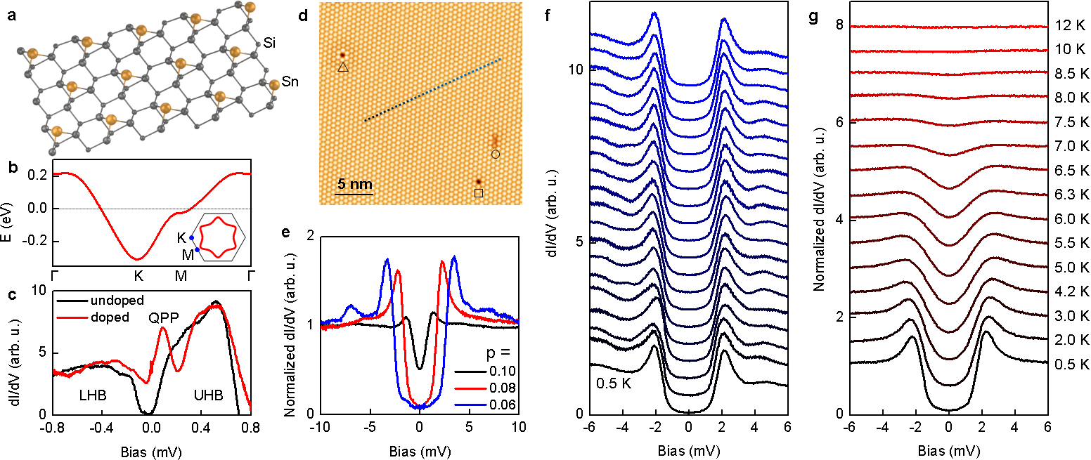
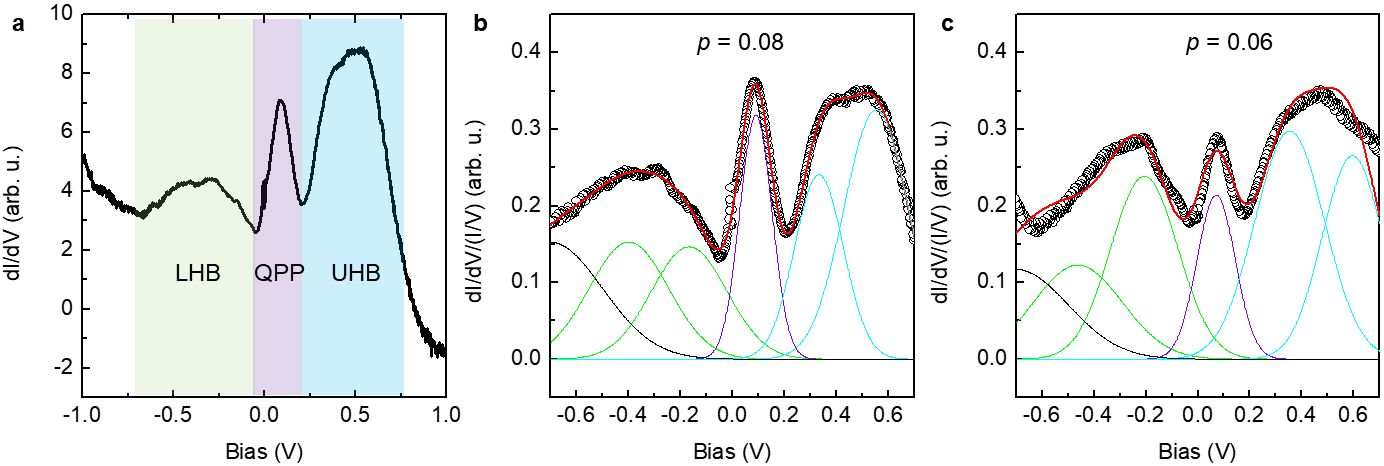
At 1/3 monolayer coverage, the Sn adatoms form a () superlattice on the Si(111) surface with one half-filled dangling-bond orbital per site and a Sn-Sn distance of 6.65 Å; see Fig.1a. All other chemical bonds in the system are passivated. The non-interacting dangling-bond surface state has a bandwidth eV (Fig. 1b), which is comparable to the on-site Hubbard interaction eV of the dangling bond orbitals [16]. As such, the system is a Mott insulator with an upper and a lower Hubbard band (UHB/LHB) straddling the Fermi level (Fig. 1c).
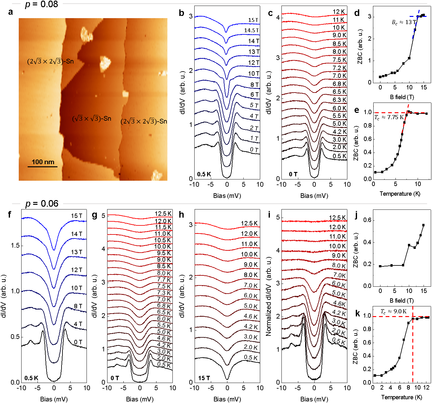
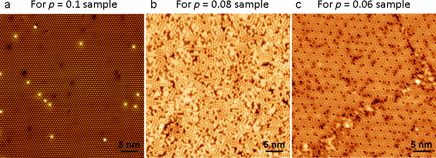
Figure 1d shows an STM image of the triangular Sn adatom lattice. The Sn atoms are clearly resolved and well ordered. The dark point defects correspond to substitutional Si adatoms (most prevalent) and Sn adatom vacancies. Holes are introduced via modulation doping, using boron-doped Si substrates with different doping levels [18, 17]. (For a discussion on dopant segregation, see Supplementary Note 1 and Supplementary Figure 1). The hole concentration in the dangling-bond surface state is estimated from the spectral weight transfer in the tunneling spectra, associated with the introduction of holes and formation of a quasiparticle peak in the Mott gap (see Fig. 1b and Extended Data Fig. 1) [18].
Fig. 1e shows the normalized tunneling spectra for excess hole concentrations of , , and , recorded at K. (The data were reported in Ref. 17.) These spectra are representative of the superconducting density of states (DOS). Here, we divided the raw tunneling spectra by the normal state spectrum obtained in a perpendicular Tesla magnetic field. This field is large enough to completely suppress the superconductivity for the and samples, which have upper critical field values of of 3 Tesla [17] and 13 Tesla, respectively (see Extended Data Fig. 2). This procedure is a bit problematic for the sample, where the upper critical field exceeds the magnetic-field capability of our instrument (15 Tesla).
The Sn adatom lattice in Figure 1a is highly ordered, while the boron dopants are located in the silicon bulk. The superconducting DOS is, therefore, spatially uniform away from localized point defects and the edges of the () domains. Fig. 1f shows a series of spectra recorded at K along the line segment in Fig. 1d. This level of homogeneity distinguishes the Sn on Si(111) system from e.g. complex oxides, which exhibit considerable electronic inhomogeneity, often in conjunction with various competing orders [23, 24].
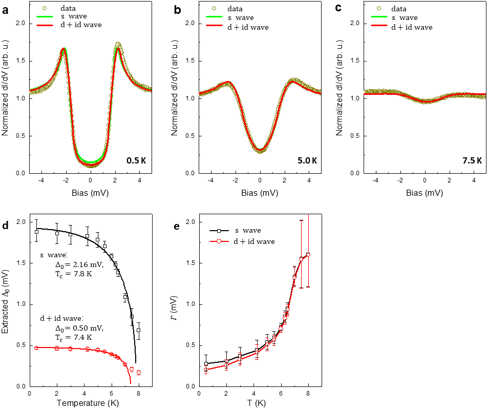
The normalized spectra of the sample are plotted as a function of temperature in Fig. 1g. The gap feature persists up to about K. Detailed Dynes fits [25] of the spectra assuming -wave and order parameter symmetries, as well as zero bias conductance measurements as a function of temperature, consistently produce a of about K with some evidence of superconducting fluctuations above (see Ref. 17, Extended Data Fig. 3, and Fig. 2a). A similar procedure for the sample produces K [17], while the of the sample was difficult to ascertain because the spectra cannot be properly normalized [ T]. We conservatively estimate its to be around K (see Extended Data Fig. 2).
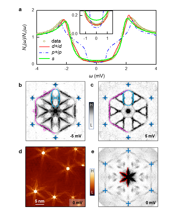
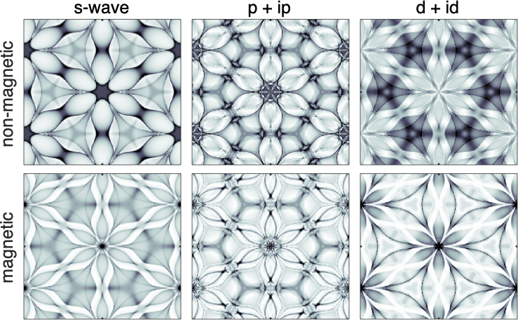
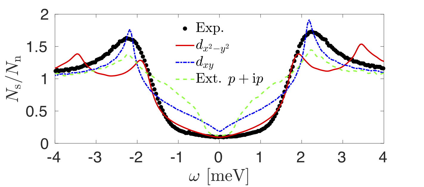
Fitting the spectra with an -wave gap produces a reasonable fit but with notable discrepancies near zero-bias. Turning to potential chiral order parameters, we find that a chiral -wave fit also agrees well with the data and even improves the fit at low energies. A chiral -wave gap clearly fails to describe the spectra, particularly at low-energy (Fig. 2a). This failure occurs because any -wave gap function must vanish at the -point by symmetry. This point corresponds to the van Hove singularity and lays close to the Fermi surface [18, 17]. It therefore affects the gap significantly, producing pronounced shoulders in the DOS that are not observed experimentally. Other parameter symmetries such as extended chiral -wave and nematic -wave symmetries (i.e., and ) do not fit the spectra either, see Supplementary Note 2. (A multigap order parameter can also be ruled out since this is a single-band system.) Only - and chiral -wave symmetries produce good results and it is not possible to conclusively discriminate between the two based on fitting alone.
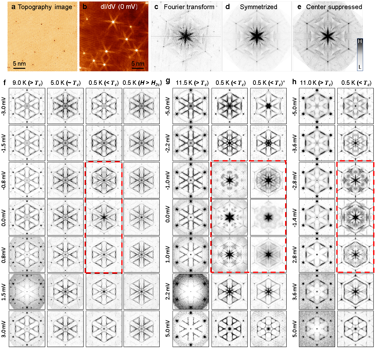
Important details about the Fermi surface and order parameter symmetry can be obtained from spectroscopic STM imaging [26]. Here, one acquires a spatial map of the differential tunneling conductance . Such maps typically reveal the presence of electronic standing waves as quasi-particles are scattered elastically by defects on the surface. The power spectrum of the differential conductance map – the QPI spectrum – then identifies the dominant scattering processes contributing to the standing wave pattern. In itinerant systems, these typically correspond to scattering wavevectors connecting different k-points on the constant energy contours (corresponding to the imaging bias) , where G is a reciprocal lattice vector of the adatom lattice.
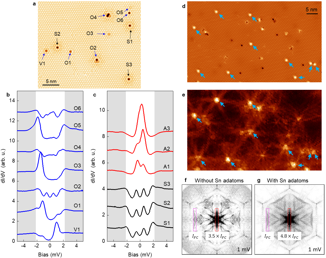
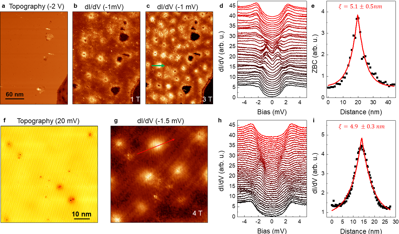
Figs. 2b, c show the K QPI spectra taken at meV bias (). Both spectra reveal the warped hexagonal Fermi contour of the normal state (), highlighted in magenta, along with several scattering replica’s () as indicated by the light blue dumbbell-shaped contours [18]. These spectra agree very well with previous calculations for the spectra in the normal state, and are fully consistent with the band structure for the Sn surface state [18]. (The presence of the quasiparticle band and its dispersion is inconsistent with an interpretation in terms of impurity band physics; see Supplementary Note 3.) Real space differential conductance maps at zero bias (Fig. 2d), i.e. deep inside the superconducting gap, reveal the existence of very strong star-like scattering features centered at the various surface defects. The corresponding Fourier map (Fig. 2e) now reveals the presence of a flower-like feature centered at and with six “petals” pointing towards the Bragg points of the () lattice, as outlined by the red contour. Meanwhile, the Fermi contour seen at meV is suppressed. This flower feature appears to be intimately related to the superconductivity; it only exists when the sample is in the superconducting state (Fig. 3a, b) and when the tunneling bias is within the superconducting gap (Fig. 2b, c, e). Hence, they are unique features of the superconducting state (see Extended Data Fig. 4 for additional QPI results).
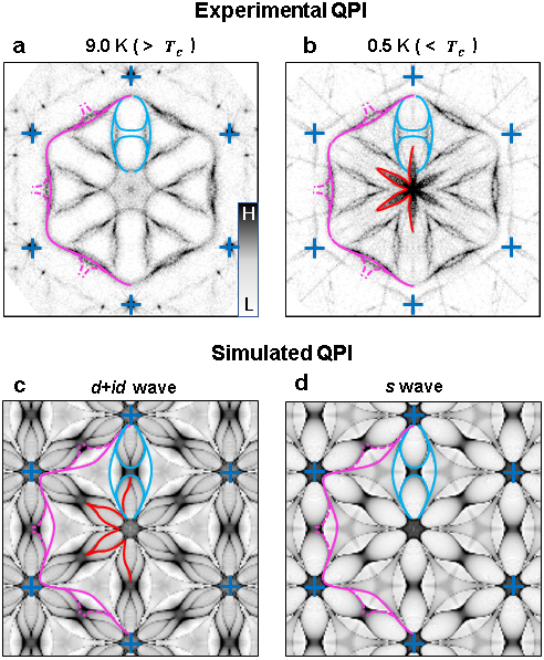
To elucidate the origin of the flower-like features, we first simulated the QPI patterns for the -wave and chiral -wave order parameters using the T-matrix formalism and assuming scattering (see Methods). Fig. 3 shows the experimental QPI spectra of the sample, along with the simulated spectra for the and -wave state. The experimental pattern in Fig. 3b is well reproduced in the calculations for the -wave pairing channel (Fig. 3c). (The theoretical features exhibit much more curvature because the calculations are based on the non-interacting band dispersion whereas the experimental band dispersion has correlation-driven band renormalizations [18].) Importantly, the flower is absent for the -wave pairing channel, as shown in Fig. 3d.
Our simulations reveal that the flower features only appear when time reversal symmetry is broken. Such would be the case for non-magnetic scattering in a chiral superconductor, as simulated above, but it could also be due to magnetic scattering in an -wave superconductor (see Extended Data Fig. 5). In particular, the star-like scattering features in the real-space QPI maps are very similar to those observed for magnetic point scatterers in -wave systems, and have been attributed to a focusing effect of magnetic bound states or Yu–Shiba–Rusinov (YSR) states due to Fermi surface anisotropy [27, 28, 29, 30, 31]. To discriminate between the -wave and -wave scenarios, it is essential to establish the nature of the defects on the surface.
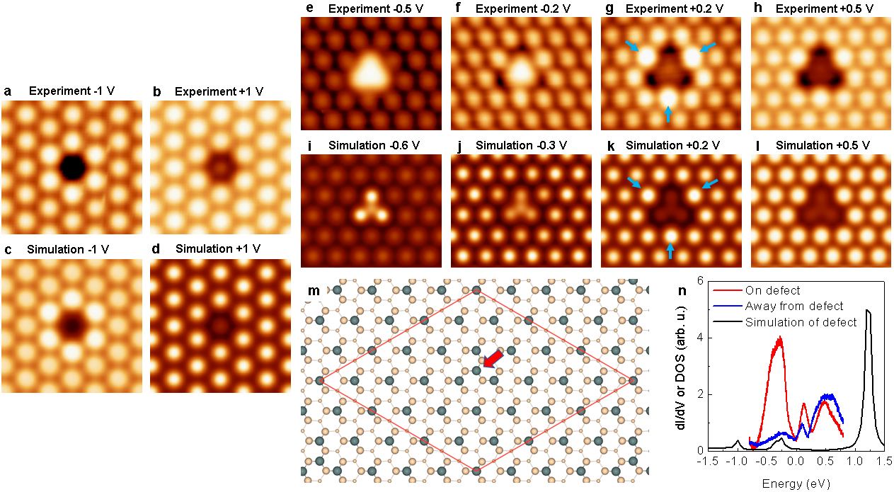
The most prevalent scattering defect on the surface is the substitutional Si adatom (replacing a Sn adatom). It shows up as a dark void in filled-state STM images and as a depressed adatom in the empty state images (see Extended Data Fig. 6). This observation indicates that the -like dangling bond orbital of the Si atom is empty, and because the adatom forms three covalent backbonds with the Si substrate, the Si adatom is expected to be non-magnetic. This is confirmed via first-principles Density Functional Theory (DFT) total-energy calculations (which show that the Si adatoms are placed 0.6 Å below the Sn adatoms) and by STM image simulations (see Methods and Extended Data Fig. 6). In addition, spin-polarized DFT calculations (see Methods) confirm the nonmagnetic nature of this defect.
It is not possible to ascertain the nature of all native defects on the surface (see Extended Data Fig. 7a) and thus rule out any magnetic scattering contribution to the QPI pattern. We therefore created a new type of defect by depositing a tiny excess amount of (nonmagnetic) Sn atoms at 120 K. STM images indicate that additional Sn adatoms are located at three-fold symmetric interstitial adatom sites, surrounded by three Sn adatoms of the 2D host lattice (see Extended Data Fig. 6). The excess Sn atoms easily move under the STM tip at tunneling biases in excess of V, indicating that they are weakly bound to the surface. The interstitial adatom location is validated by DFT total energy minimization and STM image simulations. In particular, notice the excellent agreement between the experimental and theoretical STM images, as shown in Extended Data Fig. 6. This level of agreement gives us confidence that the calculations capture the local electronic structure correctly. Importantly, spin-polarized DFT indicates that these defect centers are also nonmagnetic. The latter can be understood from the fact that the interstitial Sn atom and its three nearest neighbors have negligible contribution to the DOS at the Fermi level (Extended Data Fig. 6), thus pre-empting a potential magnetic instability.
Figure 4a plots the STS spectra across a substitutional Si defect, which reveals the existence of two in-gap states (). These states appear in pairs located symmetrically about the Fermi level reminiscent of YSR bound states though the substitutional defect is nonmagnetic. All defects on the surface we have checked produce these YSR-like in gap states albeit at different energies, including the native vacancy defects, interstitial Si, excess Sn adatoms, as well as various other defects (see Extended Data Fig. 7). This is to be expected in a chiral -wave scenario because potential and magnetic defects are both pair breaking [32, 33]. In the -wave scenario, on the other hand, one would have to assume that these defects are all magnetic [34], which seems unlikely (see Extended Data Fig. 5). Interestingly, the nonmagnetic interstitial Sn adatoms produce the strongest star-like scattering features in real-space QPI maps and the most intense flower features in the corresponding power spectrum (see Extended Data Fig. 7e-g). These enhanced scattering features near the excess Sn adatoms suggest that the -wave scenario can be dismissed because time-reversal symmetry should not be broken in such a case. Alternatively, one might suggest that nonmagnetic impurities are present in a magnetically ordered background, where they behave as magnetic impurities. Such a scenario, however, would require coexisting magnetism and superconductivity and point toward an unconventional order parameter (see also Supplementary Note 4).
Theory predicts [32, 33] that the bound states of strong scatters will be located deeper inside the gap as compared to those of weaker scatterers. Indeed, we find that the substitutional Si defects produce in-gap states at meV while interstitial Sn atoms produce states at meV. Note that the existence of gap states alone for each and every scattering defect is an indication of unconventional (i.e., non--wave) superconductivity.
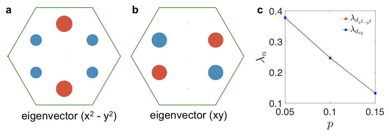
Our experimental measurements thus far point to a chiral -wave superconducting state. To demonstrate that this pairing symmetry is consistent with the known electronic structure, we performed quantum Monte Carlo dynamical cluster approximation (DCA) method [35, 36] calculations for the leading pairing instability of the ()-Sn system. Here, we consider a triangular lattice single-band Hubbard cluster embedded in a dynamical mean-field and adopt parameters previously used to describe doped [18] and undoped [16] ()-Sn (see Methods). Since our calculations are limited by the Fermion sign problem, we focused on doping levels of , , and , where we are able to access temperatures as low as meV ). For these parameters, the dominant superconducting instability indeed corresponds to degenerate and order parameters at all doping levels (see Extended Data Fig. 8). These results are consistent not only with our observations, but also several prior studies for the triangular lattice Hubbard model [37, 20] and a recent renormalization group study for Sn/Si(111) that found chiral -, -, and -wave pairing symmetries depending on the doping level and value of the nearest-neighbor Hubbard repulsion [21], with chiral -wave pairing becoming dominant when is small. We also find that the strength of the chiral -wave pairing correlations increases as the doping level decreases, consistent with observed gap magnitudes shown in Fig 1e.
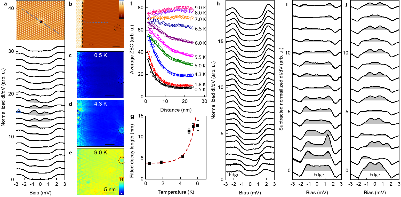
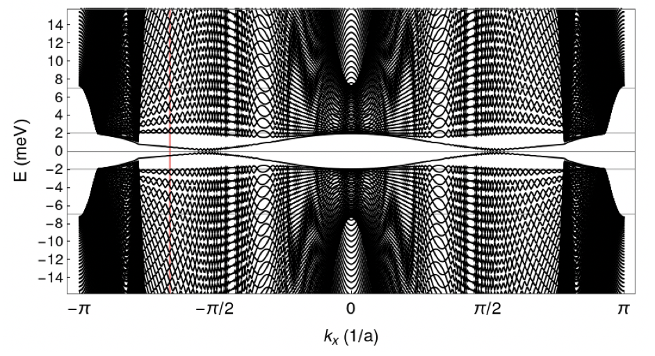
Our experimental and theoretical results are so far consistent with chiral -wave pairing. Such a pairing state should be characterized by a topological invariant [38], given by the Chern number 2 [39]. Given the nontrivial topology of the bulk pairing state, we expect the presence of chiral edge modes on sample boundaries [40], but do not expect unpaired zero energy Majorana bound states at the center of a vortex core, which arise in the case of effectively spinless pairing [5]. Indeed, we find no evidence for a Majorana zero mode at the center of a vortex core (see Extended Data Fig. 9). We did, however, find evidence consistent with the presence of chiral edge modes, as summarized in Fig.4b-i.
Figure 4b shows a topographic map near a domain wall (vertical dashed line) between the superconducting domain on the right and semiconducting domain (Ref. 41) on the left. Figs. 4c-d show registry-aligned zero-bias conductance maps over the same region of the sample at a function of temperature. The data reveal a region of increased conductance that penetrates the domain, consistent with the presence of an edge state, which grows as the temperature increases. To estimate the penetration length, we averaged the zero-bias conductance along the vertical direction and plotted it as a function of distance towards the interior, as shown in Fig. 4f. The data in the superconducting state are reasonably well described by an exponential decay (solid black lines), and we estimate that the decay length grows from nm at K to nm at K.
The increased zero-bias conductance can also be seen in the individual spectra [Fig. 4h] taken along the line approaching the domain boundary. To highlight the DOS contribution emanating from the edge, we subtracted a spectrum taken from deep in bulk from the spectra in h, as shown in Fig. 4i. The data show that the superconducting coherence peaks shift to lower energies when the edge is approached, as indicated by the formation of the peak-dip structures at about mV in the subtracted spectra. At the same time, the spectral weight in the superconducting gap increases almost uniformly as a function of energy. This behavior is consistent with an overlapping DOS from a linearly dispersing edge mode. To confirm this, we computed the chiral edge modes from a simple chiral -wave mean-field model defined on a cylinder with open boundary conditions (see methods and Extended Data Fig. 10). The simulated subtracted data, analogous to panel i are shown in Fig. 4j where they qualitatively reproduce the experimental data. We note, however, that our non-interacting model has some additional substructure in the DOS for the edge-state, which arise from the spatial structure of the edge-state wave function. While we also observe substructure in the experimental spectra, the details differ somewhat from the theory. We expect that a detailed analysis of these features will require the inclusion of interactions in our edge state model, which we leave for future work. While the enhanced zero-bias edge conductance is consistent with the presence of an edge mode, it is difficult to disentangle possible contributions from traditional coherence length effects (or inverse proximity effects [42]). Nor does the evidence imply that the edge state conductance is topological in nature, which hopefully will be elucidated in future studies.
To summarize, our combined results suggest the possibility that the hole-doped Sn/Si(111) Mott insulator system is an unconventional chiral -wave superconductor. This system exhibits a remarkable structural simplicity, with nearly perfect and strictly two-dimensional -Sn layers. It offers the ability to create, access, and characterize well-defined defect states. These aspects allowed us to identify the presence and origin of time-reversal symmetry breaking in the superconducting state. From the applied perspective, this exotic physics is accessible on a simple Si template, which can easily be altered or engineered using standard semiconductor processing or surface science approaches. Modulation-doped semiconductor surfaces and interfaces thus appear to be a promising test bed for studying and exploiting strongly correlated topological states of matter.
Methods
Sample preparation. The hole-doped ()-Sn structure was grown on three heavily boron-doped -type silicon substrates with nominal room-temperature resistivities of 0.002, 0.005, and 0.008 . They correspond to surface hole-doping concentrations of 10%, 8% and 6%, respectively, due to differences in the amount of charge transfer from the bulk to the surface [18]. These substrates were annealed to 1200∘C in ultrahigh vacuum so as to prepare atomically clean Si surfaces. Sn atoms were deposited onto the clean surface from a thermal effusion cell while keeping the substrate temperature at around 600∘C. This procedure resulted in the formation of coexisting ()-Sn and (2)-Sn domains. The maximum size (without internal domain boundary) of the ()-Sn superconducting domains on each substrate exceeds nm2. Small amount additional Sn atoms are deposited onto the surface when the sample is at 120 K, followed by a fast transfer to the STM measurement stage at lower temperature. Additional details can be found in Ref. 18.
Scanning tunneling microscopy/spectroscopy measurements. STM data were acquired using a cryogenic STM (Unisoku) that can cool the sample and tip to 400 mK in the presence of a perpendicular magnetic field of up to 15 T. Differential conductance spectra or their spatial maps were acquired using lock-in detection with a typical modulation voltage of mV and a typical modulation frequency of 673 Hz. A typical map consists of 272272 pixels measured over a 5656 nm2 surface area. QPI images are then produced by calculating the power spectral density of the Fourier transforms of the real space conductance map .
STS Fits. We fit the normalized spectra in Fig. 2a with density of states (DOS) , where denotes the DOS in the superconducting (normal) state. Here,
| (1) |
is the non-interacting Green’s function in Nambu space, are Pauli matrices, is the bare band dispersion, and parameterizes the superconducting gap function in Nambu space . Note, for the chiral -wave case, the space corresponds to the vector .
To model the Sn surface state, we adopted the tight-binding model derived in Ref. 16, which is derived from electronic structure calculations. The band dispersion is
| (2) |
with meV, , , , , and . Note that we adjusted the chemical potential to put the van Hove singularity meV below [18].
To model the normal state, we set . To model an -wave superconductor, we set . To model the chiral - and -wave cases, we set , where and [43]
for chiral -wave pairing and
for chiral -wave pairing. We have also fit the spectra with nematic -wave order parameters (see Supplementary Note 2) and found that they are unable to reproduce the experimental spectra.
We then fit theoretical DOS to the STS data treating and as fitting parameters. The best fits shown in Fig. 2a are obtained with , , and for the -, chiral -, and chiral -wave cases, respectively, in units of meV.
Quasiparticle interference calculations. The QPI spectra are calculated using the Born approximation to the -matrix formalism, with a single point-like potential located at the origin. The Fourier transform of the modulation in the electron density is given by
| (3) |
where , is the Green’s function given by Eq. (1), is the impurity potential, and and are the bare band dispersion and superconducting order parameter, respectively. We considered both magnetic () and nonmagnetic () scatterers, whose strengths are parameterized by . For the superconducting gap, we considered many different pairing symmetries, as parameterized above (see Extended Data Figure 5).
DFT calculations.
Plane-wave DFT calculations were implemented using the Quantum Espresso open source computer code [44]. We have used the PBE exchange-correlation functional [45] and the ultrasoft pseudopotentials provided by the code [46, 47]. The energy cutoff for the plane waves is 40 Ry. While DFT cannot capture the Mott state of the ()-Sn system, it accurately captures the ground state structure [48]. We employed a () supercell with 6 Si layers and 27 Sn adatoms in positions. In total, there are 594 atoms in the unit cell. To simulate the substitutional Si defect, we replaced one of the 27 Sn adatoms with a Si atom. Based on the experimental results, the interstitial Sn adatom is placed at the center of an equilateral triangle formed by three adjacent Sn atoms of the original ()-Sn surface. Hence the total number of Sn atoms is 28; see Extended Data Fig. 6. The bottom two Si layers and the H layer are fixed in these simulations. The () first Brillouin zone was sampled with a Monkhorst-Pack (MP) grid [49] and the geometry is relaxed until the forces are lower than 0.001 Ry/Bohr. In the total-energy minimized geometry, the Sn atoms forming the triangle are located Å above the atoms of the ()-Sn layer. The additional Sn adatom at the center of the triangle is located Å above the ()-Sn layer, i.e., Å below its nearest neighbors.
STM image simulations.
The simulated STM images for both defect structures were calculated using the Keldysh-Green Function formalism [50] together with the Fireball local-orbital DFT Hamiltonian [51]. This procedure has been successfully used in many works before (e.g. see Ref. 52). In our simulations, a standard W tip is placed at a distance of 5 Å above the surface and images were generated for tunneling parameters close to the experimental conditions. In Extended Data Fig. 6 we show the experimental and simulated images side by side, showing excellent agreement for the chosen tunneling parameters. The STM images can be correlated to the different atomic heights and Projected Density of States (PDOS) on the different atoms. The PDOS on the interstitial Sn adatom, calculated with the local-orbital DFT code, is shown in Extended Data Fig. 6. A similar procedure was implemented for the substitutional Si defect. The corresponding experimental and theoretical images are shown in Extended Data Fig. 6 and are in good agreement.
DCA calculations.
DCA calculations for the triangular lattice single-band Hubbard model were performed with the DCA++ package [36] using a continuous-time quantum Monte Carlo impurity solver. Here, we consider a cluster of Sn atoms with the bare band structure as given in Ref. 16 but including only up to third nearest neighbor hopping (i.e. ), since the cluster cannot support longer range hopping. We further set eV [16]. The DCA calculations measured the single-particle Green’s function and two-particle Green’s function in the particle-particle channel with zero momentum and frequency transfer. From that, we extracted the irreducible particle-particle vertex and then solved the Bethe-Salpeter equation (BSE) to obtain the leading eigenvalues and eigenvectors in the particle-particle channel, as described in Ref. 35. The pairing symmetry of the dominant superconducting instability can be extracted from the leading eigenvector.
Edge state calculations. We compute the topological edge states of the chiral superconductor by solving the same triangular lattice model defined in Eq. (2) but defined on a cluster with open boundary conditions in the direction and periodic boundary condition in the direction, as shown in Extended Data Fig. 10. Introducing the labels for the chains stacked in the direction, and for the momentum along the edge, the Hamiltonian can be written as
| (4) |
where is a Nambu spinor collecting electron and hole degree of freedom. The Hamiltonian matrix describes how chains and are coupled. It is convenient to decompose as (momentum dependence is suppressed)
| (5) |
where captures the coupling of -th nearest neighbor chains and satisfies . Here denotes the extent of the coupling; if only first nearest neighbor chains are coupled . In the present problem . The matrices are given by
| (6) |
The Hamiltonian defines a Schrödinger equation given by
| (7) |
where is the wave function with electron and hole components and . We solve this system of equations numerically on a finite slab to obtain the quasiparticle spectrum in the presence of an edge. Here is an index to label eigenvalues at given . For a system with chains one has .
Finally, we compute the chain-resolved local density of states as
| (8) |
Acknowledgments: We thank C. D. Batista, P. J. Hirschfeld, P. Kent, A. Tennant, and R. Zhang for fruitful discussions. The experimental work and QPI calculations were supported by the Guangdong Basic and Applied Basic Research Foundation, Ref No. 2021A1515012034 and by the Office of Naval Research under Grant No. N00014-18-1-2675. F. M. acknowledges the support by NSFC (No. 12174456) and the Guangdong Basic and Applied Basic Research Foundation (grants no. 2020B1515020009) C. G. acknowledges financial support from the Community of Madrid through the project NANOMAGCOST CM-PS2018/NMT-4321 and the computer resources at Altamira, and the technical support provided by the Instituto de Física de Cantabria (IFCA), Project: QHS-2021-3-0005. J. O. acknowledges financial support by the Spanish Ministry of Science and Innovation through grants MAT2017-88258-R and CEX2018-000805-M (María de Maeztu Programme for Units of Excellence in R&D). The DCA calculations were supported by the Scientific Discovery through Advanced Computing (SciDAC) program funded by the U.S. Department of Energy, Office of Science, Advanced Scientific Computing Research and Basic Energy Sciences, Division of Materials Sciences and Engineering. This research also used resources of the Oak Ridge Leadership Computing Facility, which is a DOE Office of Science User Facility supported under Contract DE-AC05-00OR22725.
Data availability: The data supporting this study will be made available upon request.
Code availability: The DCA++ code used for this project can be obtained at https://github.com/CompFUSE/DCA. The Quantum Espresso code can be obtained from https://www.quantum-espresso.org/. The Fireball code can be obtained from https://github.com/fireball-QMD. The other codes supporting this study will be made available upon request.
Author contributions: F. M., X. W. contributed equally to this work. F. M., X. W., C. C and K. D. W. prepared the samples and performed the STM experiments. P. M. and T. A. M. performed the DCA calculations. J. S. and J. W. F. V. performed edge state calculations. C. G. and J. O. performed the DFT calculations and STM image simulations. S. J. performed the QPI calculations. S. J. and H. H. W. conceived and supervised the project, and wrote the manuscript with input from all authors.
Competing interests: The authors declare that they have no competing financial interests.
Correspondence and requests for materials should be addressed to K.D. Wang (email: wangkd@sustech.edu.cn), S.J. (email: sjohn145@utk.edu), or H.H.W. (email: hanno@utk.edu).
References
- Bardeen et al. [1957] J. Bardeen, L. N. Cooper, and J. R. Schrieffer, Theory of superconductivity, Phys. Rev. 108, 1175 (1957).
- Kohn and Luttinger [1965] W. Kohn and J. M. Luttinger, New mechanism for superconductivity, Phys. Rev. Lett. 15, 524 (1965).
- Scalapino [2012] D. J. Scalapino, A common thread: The pairing interaction for unconventional superconductors, Rev. Mod. Phys. 84, 1383 (2012).
- Tsuei and Kirtley [2000] C. C. Tsuei and J. R. Kirtley, Pairing symmetry in cuprate superconductors, Rev. Mod. Phys. 72, 969 (2000).
- Read and Green [2000] N. Read and D. Green, Paired states of fermions in two dimensions with breaking of parity and time-reversal symmetries and the fractional quantum Hall effect, Phys. Rev. B 61, 10267 (2000).
- Joynt and Taillefer [2002] R. Joynt and L. Taillefer, The superconducting phases of , Rev. Mod. Phys. 74, 235 (2002).
- Nandkishore et al. [2012] R. Nandkishore, L. S. Levitov, and A. V. Chubukov, Chiral superconductivity from repulsive interactions in doped graphene, Nature Physics 8, 158 (2012).
- Kallin [2012] C. Kallin, Chiral -wave order in Sr2RuO4, Reports on Progress in Physics 75, 042501 (2012).
- Black-Schaffer [2012] A. M. Black-Schaffer, Edge properties and Majorana fermions in the proposed chiral -wave superconducting state of doped graphene, Phys. Rev. Lett. 109, 197001 (2012).
- Kiesel et al. [2013] M. L. Kiesel, C. Platt, W. Hanke, and R. Thomale, Model evidence of an anisotropic chiral -wave pairing state for the water-intercalated superconductor, Phys. Rev. Lett. 111, 097001 (2013).
- Black-Schaffer and Honerkamp [2014] A. M. Black-Schaffer and C. Honerkamp, Chiral -wave superconductivity in doped graphene, Journal of Physics: Condensed Matter 26, 423201 (2014).
- Kallin and Berlinsky [2016] C. Kallin and J. Berlinsky, Chiral superconductors, Reports on Progress in Physics 79, 054502 (2016).
- Mackenzie et al. [2017] A. P. Mackenzie, T. Scaffidi, C. W. Hicks, and Y. Maeno, Even odder after twenty-three years: the superconducting order parameter puzzle of Sr2RuO4, npj Quantum Materials 2, 40 (2017).
- Pustogow et al. [2019] A. Pustogow, Y. Luo, A. Chronister, Y. S. Su, D. A. Sokolov, F. Jerzembeck, A. P. Mackenzie, C. W. Hicks, N. Kikugawa, S. Raghu, E. D. Bauer, and S. E. Brown, Constraints on the superconducting order parameter in Sr2RuO4 from oxygen-17 nuclear magnetic resonance, Nature 574, 72 (2019).
- Jiao et al. [2020] L. Jiao, S. Howard, S. Ran, Z. Wang, J. O. Rodriguez, M. Sigrist, Z. Wang, N. P. Butch, and V. Madhavan, Chiral superconductivity in heavy-fermion metal UTe2, Nature 579, 523 (2020).
- Li et al. [2013] G. Li, P. Höpfner, J. Schäfer, C. Blumenstein, S. Meyer, A. Bostwick, E. Rotenberg, R. Claessen, and W. Hanke, Magnetic order in a frustrated two-dimensional atom lattice at a semiconductor surface, Nature Communications 4, 1620 (2013).
- Wu et al. [2020] X. Wu, F. Ming, T. S. Smith, G. Liu, F. Ye, K. Wang, S. Johnston, and H. H. Weitering, Superconductivity in a hole-doped Mott-insulating triangular adatom layer on a silicon surface, Phys. Rev. Lett. 125, 117001 (2020).
- Ming et al. [2017a] F. Ming, S. Johnston, D. Mulugeta, T. S. Smith, P. Vilmercati, G. Lee, T. A. Maier, P. C. Snijders, and H. H. Weitering, Realization of a hole-doped Mott insulator on a triangular silicon lattice, Phys. Rev. Lett. 119, 266802 (2017a).
- Lee et al. [2006] P. A. Lee, N. Nagaosa, and X.-G. Wen, Doping a Mott insulator: Physics of high-temperature superconductivity, Rev. Mod. Phys. 78, 17 (2006).
- Cao et al. [2018] X. Cao, T. Ayral, Z. Zhong, O. Parcollet, D. Manske, and P. Hansmann, Chiral -wave superconductivity in a triangular surface lattice mediated by long-range interaction, Phys. Rev. B 97, 155145 (2018).
- Wolf et al. [2022] S. Wolf, D. Di Sante, T. Schwemmer, R. Thomale, and S. Rachel, Triplet superconductivity from nonlocal Coulomb repulsion in an atomic Sn layer deposited onto a Si(111) substrate, Phys. Rev. Lett. 128, 167002 (2022).
- Zahedifar and Kratzer [2019] M. Zahedifar and P. Kratzer, Phonon-induced electronic relaxation in a strongly correlated system: The Sn/Si(111) adlayer revisited, Phys. Rev. B 100, 125427 (2019).
- Howald et al. [2003] C. Howald, H. Eisaki, N. Kaneko, and A. Kapitulnik, Coexistence of periodic modulation of quasiparticle states and superconductivity in Bi2Sr2CaCu2O8+δ, Proceedings of the National Academy of Sciences 100, 9705 (2003).
- Vershinin et al. [2004] M. Vershinin, S. Misra, S. Ono, Y. Abe, Y. Ando, and A. Yazdani, Local ordering in the pseudogap state of the high- superconductor Bi2Sr2CaCu2O8+δ, Science 303, 1995 (2004).
- Dynes et al. [1978] R. C. Dynes, V. Narayanamurti, and J. P. Garno, Direct measurement of quasiparticle-lifetime broadening in a strong-coupled superconductor, Phys. Rev. Lett. 41, 1509 (1978).
- Petersen et al. [2000] L. Petersen, P. Hofmann, E. Plummer, and F. Besenbacher, Fourier transform–STM: determining the surface Fermi contour, Journal of Electron Spectroscopy and Related Phenomena 109, 97 (2000).
- Yu [1965] L. Yu, Bound state in superconductors with paramagnetic impurities, Wu Li Hsueh Pao (China) Supersedes Chung-Kuo Wu Li Hsueh For English translation see Chin. J. Phys. (Peking) (Engl. Transl.) 21 (1965).
- Shiba [1968] H. Shiba, Classical Spins in Superconductors, Progress of Theoretical Physics 40, 435 (1968).
- Rusinov [1969] A. I. Rusinov, Superconductivity near a paramagnetic impurity, JETP Lett. (USSR) (Engl. Transl.), 9: 85-7 (Jan. 20, 1969). (1969).
- Ménard et al. [2015] G. C. Ménard, S. Guissart, C. Brun, S. Pons, V. S. Stolyarov, F. Debontridder, M. V. Leclerc, E. Janod, L. Cario, D. Roditchev, P. Simon, and T. Cren, Coherent long-range magnetic bound states in a superconductor, Nature Physics 11, 1013 (2015).
- Kim et al. [2020] H. Kim, L. Rózsa, D. Schreyer, E. Simon, and R. Wiesendanger, Long-range focusing of magnetic bound states in superconducting lanthanum, Nature Communications 11, 4573 (2020).
- Wang and Wang [2004] Q.-H. Wang and Z. D. Wang, Impurity and interface bound states in and superconductors, Phys. Rev. B 69, 092502 (2004).
- Mashkoori et al. [2017] M. Mashkoori, K. Björnson, and A. M. Black-Schaffer, Impurity bound states in fully gapped -wave superconductors with subdominant order parameters, Scientific Reports 7, 44107 (2017).
- Anderson [1959] P. Anderson, Theory of dirty superconductors, Journal of Physics and Chemistry of Solids 11, 26 (1959).
- Maier et al. [2006] T. A. Maier, M. S. Jarrell, and D. J. Scalapino, Structure of the pairing interaction in the two-dimensional Hubbard model, Phys. Rev. Lett. 96, 047005 (2006).
- Hähner et al. [2020] U. R. Hähner, G. Alvarez, T. A. Maier, R. Solcà, P. Staar, M. S. Summers, and T. C. Schulthess, DCA++: A software framework to solve correlated electron problems with modern quantum cluster methods, Computer Physics Communications 246, 106709 (2020).
- Chen et al. [2013] K. S. Chen, Z. Y. Meng, U. Yu, S. Yang, M. Jarrell, and J. Moreno, Unconventional superconductivity on the triangular lattice Hubbard model, Phys. Rev. B 88, 041103 (2013).
- Volovik [1997] G. E. Volovik, On edge states in superconductors with time inversion symmetry breaking, Journal of Experimental and Theoretical Physics Letters 66, 522 (1997).
- Laughlin [1998] R. B. Laughlin, Magnetic induction of order in high- superconductors, Phys. Rev. Lett. 80, 5188 (1998).
- Senthil et al. [1999] T. Senthil, J. B. Marston, and M. P. A. Fisher, Spin quantum Hall effect in unconventional superconductors, Phys. Rev. B 60, 4245 (1999).
- Ming et al. [2017b] F. Ming, D. Mulugeta, W. Tu, T. S. Smith, P. Vilmercati, G. Lee, Y.-T. Huang, R. D. Diehl, P. C. Snijders, and H. H. Weitering, Hidden phase in a two-dimensional Sn layer stabilized by modulation hole doping, Nature Communications 8, 14721 (2017b).
- De Gennes [1964] P. G. De Gennes, Boundary effects in superconductors, Rev. Mod. Phys. 36, 225 (1964).
- Zhou and Wang [2008] S. Zhou and Z. Wang, Nodal pairing and topological phases on the triangular lattice of : Evidence for an unconventional superconducting state, Phys. Rev. Lett. 100, 217002 (2008).
- Giannozzi et al. [2009] P. Giannozzi, S. Baroni, N. Bonini, M. Calandra, R. Car, C. Cavazzoni, D. Ceresoli, G. L. Chiarotti, M. Cococcioni, I. Dabo, A. D. Corso, S. de Gironcoli, S. Fabris, G. Fratesi, R. Gebauer, U. Gerstmann, C. Gougoussis, A. Kokalj, M. Lazzeri, L. Martin-Samos, N. Marzari, F. Mauri, R. Mazzarello, S. Paolini, A. Pasquarello, L. Paulatto, C. Sbraccia, S. Scandolo, G. Sclauzero, A. P. Seitsonen, A. Smogunov, P. Umari, and R. M. Wentzcovitch, QUANTUM ESPRESSO: a modular and open-source software project for quantum simulations of materials, Journal of Physics: Condensed Matter 21, 395502 (2009).
- Perdew et al. [1996] J. P. Perdew, K. Burke, and M. Ernzerhof, Generalized gradient approximation made simple, Phys. Rev. Lett. 77, 3865 (1996).
- Goedecker et al. [1996] S. Goedecker, M. Teter, and J. Hutter, Separable dual-space gaussian pseudopotentials, Phys. Rev. B 54, 1703 (1996).
- Hartwigsen et al. [1998] C. Hartwigsen, S. Goedecker, and J. Hutter, Relativistic separable dual-space gaussian pseudopotentials from H to Rn, Phys. Rev. B 58, 3641 (1998).
- Pérez et al. [2001] R. Pérez, J. Ortega, and F. Flores, Surface soft phonon and the phase transition in and , Phys. Rev. Lett. 86, 4891 (2001).
- Monkhorst and Pack [1976] H. J. Monkhorst and J. D. Pack, Special points for Brillouin-zone integrations, Phys. Rev. B 13, 5188 (1976).
- Blanco et al. [2004] J. M. Blanco, C. González, P. Jelínek, J. Ortega, F. Flores, and R. Pérez, First-principles simulations of STM images: From tunneling to the contact regime, Phys. Rev. B 70, 085405 (2004).
- Lewis et al. [2011] J. P. Lewis, P. Jelínek, J. Ortega, A. A. Demkov, D. G. Trabada, B. Haycock, H. Wang, G. Adams, J. K. Tomfohr, E. Abad, H. Wang, and D. A. Drabold, Advances and applications in the FIREBALL ab initio tight-binding molecular-dynamics formalism, physica status solidi (b) 248, 1989 (2011).
- González et al. [2004] C. González, P. C. Snijders, J. Ortega, R. Pérez, F. Flores, S. Rogge, and H. H. Weitering, Formation of atom wires on vicinal silicon, Phys. Rev. Lett. 93, 126106 (2004).
- Ming et al. [2018] F. Ming, T. S. Smith, S. Johnston, P. C. Snijders, and H. H. Weitering, Zero-bias anomaly in nanoscale hole-doped Mott insulators on a triangular silicon surface, Phys. Rev. B 97, 075403 (2018).
- Headrick et al. [1989] R. L. Headrick, I. K. Robinson, E. Vlieg, and L. C. Feldman, Structure determination of the Si(111):B(3×3)R30° surface: Subsurface substitutional doping, Phys. Rev. Lett. 63, 1253 (1989).
- Lyo et al. [1989] I.-W. Lyo, E. Kaxiras, and P. Avouris, Adsorption of boron on Si(111): Its effect on surface electronic states and reconstruction, Phys. Rev. Lett. 63, 1261 (1989).
- Shi et al. [2002] H. Q. Shi, M. W. Radny, and P. V. Smith, Electronic structure of the surface, Phys. Rev. B 66, 085329 (2002).
- Andrade et al. [2015] D. P. Andrade, R. H. Miwa, B. Drevniok, P. Drage, and A. B. McLean, Surface and near surface defects in -doped Si(1 1 1), Journal of Physics: Condensed Matter 27, 125001 (2015).
- Lee et al. [2014] J.-H. Lee, X.-Y. Ren, Y. Jia, and J.-H. Cho, Antiferromagnetic superexchange mediated by a resonant surface state in Sn/Si(111), Phys. Rev. B 90, 125439 (2014).
Extended data figures and tables
Supplementary Notes and Figures
Supplementary Note 1: Modulation hole doping and dopant segregation
Ming et al. [18] have shown that the formation of the ()-Sn surface is accompanied by a downward band bending near the surface of the boron-doped p-type Si substrate. This behavior means that the valence band holes in the subsurface region transfer to the dangling bond surface state. (Holes move up to lower their electronic energy; alternatively, the Sn adatoms give up some electrons to fill the hole states in bulk). This process is self-limiting, however, as a space charge layer dipole gradually builds up and prevents further charge transfer. (This band bending scenario is analogous to the formation of a depletion layer in semiconductor heterostructures.) The hole-doped surface state thus represents the total energy minimum. Carrier freeze-out in bulk Si at low temperature is irrelevant for our experiments as the relevant holes reside in a metallic surface state well above the valence band maximum (the quasi-particle band), which is formed during or after the growth stage (when cooling to room temperature). These holes are itinerant.
The substrate cleaning procedure involves a high temperature annealing step that unavoidably leads to boron accumulation near the surface layers. Boron segregation ultimately produces a surface before depositing Sn. Here, the boron atoms reside at the S5 site in the second layer directly below the Si adatom, see e.g., Refs. 54 and 55. The dangling bond surface state of the Si adatom is empty; see Ref. 55. Supplementary Figure 1 provides images of the boron segregated substrates obtained before Sn deposition. Unless the boron is fully segregated, forming a structure, the substrate surface can be quite inhomogeneous or it exhibits the native Si(111) reconstruction at the lowest doping level.
Crucially, after depositing Sn at C and subsequently cooling, the ()-Sn surface is very homogeneous (see Fig. 1 of the main text), both in topographic imaging and in imaging, which show only small amounts of disorder. Either the boron atoms diffuse deeper into the bulk during the formation of the ()-Sn surface at high temperature, or they form an ordered subsurface layer where the boron atoms occupy the S5 lattice locations. We cannot verify the first possibility directly, but the second possibility can be ruled out easily because the Sn-derived surface state band would be empty in this case (see Supplementary Note 3). Instead, we find it is almost half-filled. The latter can be inferred from the very close match between the theoretical and experimental dispersion relations, including the Fermi level crossings, as shown in Fig. 3k and 3l of Ref. 18. Our results are also fully consistent with a density functional theory (DFT) calculation where the boron atoms reside in deeper layers, and the surface state becomes hole-doped (see Supplementary Note 3).
We reiterate that the hole-doped ()-Sn surface is structurally and electronically homogeneous (Fig. 1). Hole doping produces a single Fermi surface contour that is reproduced in our QPI image simulations based on the theoretical (DFT) band dispersion of the Sn-derived dangling-bond surface state. These observations demonstrate the efficacy of the modulation doping approach. Note that it would be inconceivable that a chemically disordered mix of Sn and B would produce such a result.
Supplementary Note 2: Additional fits to the STS spectra
To rule out other possible pairing scenarios, we performed additional fits to the STS spectra assuming nematic and order parameters, as well as an extended case. The latter case includes nearest- and next-nearest-neighbor pairing as parameterized in Ref. [43]. All three order parameters produce unsatisfactory fits of the STS spectra, as shown in Supplementary Figure 2. The qualitative discrepancy here is caused by the fact that each of these order parameters produces a significant amount of anisotropy on the Fermi surface, with nodes for the -wave cases.
We have also explicitly checked the scenario where the pairing interaction produces a momentum-dependent -wave gap that resembles the chiral -wave case. To do so, we introduced an -wave gap defined as .
This substitution produces a real valued gap whose momentum dependence perfectly mimics the anisotropy of the chiral -wave case but lacks the phase information. Defined in this way, is a six-fold symmetric -wave order parameter that produces an STS fit indistinguishable from our chiral -wave case. This case does not reproduce the flower-like features observed in the QPI spectra. These results make it clear that the data are inconsistent with an anisotropic -wave, chiral , and nematic -wave order parameters.
Supplementary Note 3: DFT calculations for the B-doped surface
DFT calculations for the boron saturated () substrate surface (without Sn) can be found in Refs. 56 and 57. The surface is gapped and the only state in the gap is the adatom dangling state that is located well above the Fermi level near the conduction band continuum.
In this work, we performed new plane-wave DFT calculations for a 10-layer Si slab terminated with the ()-Sn structure on one side and saturated with hydrogen on the other. We considered the following scenarios for the ()-Sn surface:
-
a)
no boron doping;
-
b)
one boron atom per unit cell, where the boron is residing directly below the Sn adatoms;
-
c)
one boron atom per unit cell, where the boron atom is located in the fifth Si layer (corresponding to an extremely high bulk concentration of about boron atoms per cm3); and
-
d)
one boron atom per unit cell, again with the boron atom residing in the fifth layer.
(In the calculations, we did not consider the scenario with one boron atom located at one of the four S5 lattice locations in the unit cell as this would produce inequivalent lattice sites within the unit cell, whereas the lattice seen by STM is a perfect (). Results are shown in Supplementary Figure 3.
Scenario a) (Supplementary Figure 3a), produces a single Sn-derived dangling bond surface state inside the bulk band gap of Si. The band is half-filled (as expected with one electron per dangling bond site) and is subject to the Mott transition resulting in the upper and lower Hubbard band seen in experiment; see e.g. Refs. 18 and 16.
In scenario b) (Supplementary Figure 3b), the Sn-derived dangling bond surface state is located entirely above the Fermi level. Here, the dangling bond electrons are fully compensated by the holes in the subsurface layer, and the surface is semiconducting. To put it differently, each boron atom at the S5 lattice location accepts the dangling bond charge of the Sn atom sitting right above and becomes a negative acceptor ion. This scenario is inconsistent with the observation of the remnant lower and upper Hubbard bands in the STS spectra and the observation of a dispersive QPP state in the QPI spectra in the doped system.
Scenario c) (Supplementary Figure 3c) reveals the same band, but this time it is crossing the Fermi level. The Fermi level is about 0.1 eV below the van Hove singularity at the -point. This situation represents a heavily overdoped case, an artifact of the small supercell used in the calculation. Experimentally, the Fermi level is located 7 meV above the van Hove singularity [18]. The calculation furthermore places the Fermi level below the top of the bulk Si valence band, while in the experiment, the Fermi level is located 0.5 eV above the valence band maximum; see supplementary information in Ref. 18.
Finally, scenario d) (Supplementary Figure 3d) is approximately consistent with experimental observations. Because the unit cell was quadrupled in this calculation, the doping level is reduced by a factor of four, and there are now four Sn bands inside the Si band gap instead of one. These bands originate from the same Sn-derived dangling bond surface state, backfolded about the Brillouin zone. (In experiment, we only see one band as the translational symmetry is .) Importantly, the Fermi level is about 0.18 eV above the valence band maximum, and the band filling is . This concentration corresponds to a hole doping level of or , still exceeding the experimentally determined doping level by about a factor of two. Due to the Mott correlations, the surface state splits into an upper and lower Hubbard band and, because the surface state is no longer half-filled, a quasi particle peak appears in between; see Ref. 18. A similar calculation for a unit cell (not shown) produces a hole concentration of or , which is close to that of the sample. Here the Fermi level is about 0.30 eV above the valence band maximum. Calculations for lower doping levels would require even larger super cells, but the trend is clear: The holes are all located in the Sn dangling bonds, except at extremely high doping levels where the Fermi level crosses the valence band maximum, creating holes at the top of the valence band near the -point. Experimentally, however, the valence band maximum is located 0.5 eV below the Fermi level, meaning there are no bulk valence band holes.
The important conclusion here is that these different doping scenarios affect the location of the Sn-derived surface state and chemical potential inside the gap. The only band crossing the Fermi level is the Sn-derived dangling bond surface state at the experimentally realizable doping levels. While there are many other possible distributions of the boron atoms, it is critically important to recognize that the surface is structurally and electronically homogeneous (see Fig. 1, main text). The boron dopants are likely located in deeper layers, not at the S5 lattice locations of the second layer (scenario b).
The DFT calculations also rule out the possibility of a boron impurity band crossing the Fermi level. The fact that the DFT calculations do not produce any B-derived bands in the Si band gap, indicates that the B impurity states are not in the band gap. There is no evidence of coherent hopping between B sites, which would also be very unlikely for a disordered boron distribution, as the potential would no longer be periodic.
Supplementary Note 4: Nonmagnetic impurities in a magnetically ordered background
One might argue that because the undoped Sn/Si(111) system has a striped antiferromagnetic order [16, 58], magnetic order might persist upon hole doping, in which case a nonmagnetic defect could be viewed as a magnetic perturbation. For this scenario to be true, the antiferromagnetism would have to coexist with superconductivity within a superconducting domain. There are no known examples of such coexistence in -wave superconductors. Hence, this would seem incompatible with a conventional -wave order parameter. Instead, it would suggest an unconventional pairing symmetry. A chiral state is then naturally expected for the triangular lattice geometry.
Finally, we note that the size and shape of the Fermi surface inferred from the QPI spectra for the doped system is consistent with DFT calculations for a paramagnetic Sn lattice; it does not have any indications of zone-folding that must accompany any antiferromagetic ordering.