Evidence for spin-polarized bound states in
semiconductor-superconductor-ferromagnetic insulator islands
Abstract
We report Coulomb blockade transport studies of semiconducting InAs nanowires grown with epitaxial superconducting Al and ferromagnetic insulator EuS on overlapping facets. Comparing experiment to a theoretical model, we associate cotunneling features in even-odd bias spectra with spin-polarized Andreev levels. Results are consistent with zero-field spin splitting exceeding the induced superconducting gap. Energies of subgap states are tunable on either side of zero via electrostatic gates.
In hybrid quantum devices with both ferromagnetic and superconducting components, competition to align electron spins or pair them into singlets can result in complex ground states and corresponding electrical properties Meservey and Tedrow (1994); Buzdin (2005); Sau et al. (2010); Eschrig (2011); Li et al. (2014); Linder and Robinson (2015); Strambini et al. (2017); Bergeret et al. (2018); Manna et al. (2020). Recently, coexistence of proximity-induced superconductivity and ferromagnetism have been demonstrated in hybrid semiconducting nanowires Vaitiekėnas et al. (2021). Coulomb-blockade spectroscopy of superconducting quantum dots provides a window into subgap spectra Higginbotham et al. (2015) and their spin structure Prada et al. (2020).
Multiple Andreev scatterings at superconducting boundaries of a small normal conductor give rise to Andreev bound states (ABSs) Prada et al. (2020). The states can carry supercurrent through the normal region and appear in tunneling spectroscopy as discrete levels below the superconducting gap Pillet et al. (2010); Nichele et al. (2020). Coulomb effects modify transport via ABSs Grove-Rasmussen et al. (2009); Chang et al. (2013), for instance resulting in supercurrent reversal van Dam et al. (2006); Jørgensen et al. (2007). When magnetic fields Lee et al. (2014); Shen et al. (2018) or magnetic materials Heinrich et al. (2018) are involved, spin-degenerate ABSs split and becomes spin selective, as seen in tunneling spectroscopy Whiticar et al. (2021) and circuit quantum electrodynamics measurements Hays et al. (2020). The spin-active interface between a superconductor and, for example, a ferromagnetic insulator Tokuyasu et al. (1988) can also lead to spin-split ABSs Hübler et al. (2012) or, in some cases, triplet superconductivity Diesch et al. (2018).
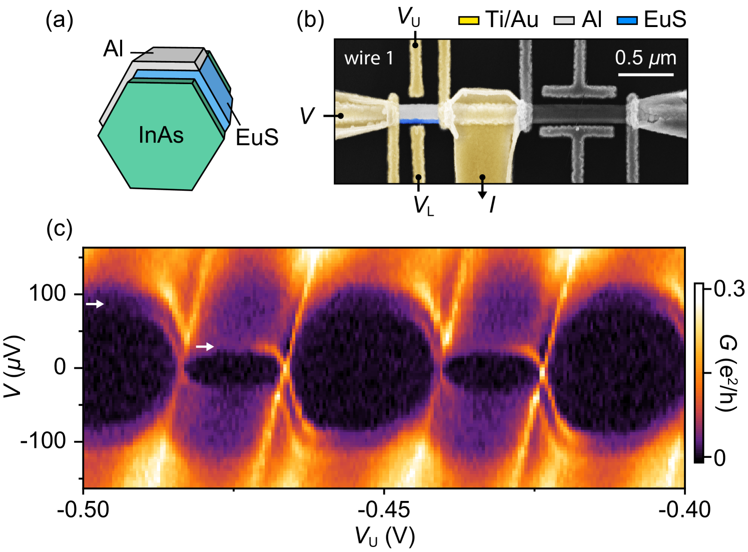
Recently, a new class of triple-hybrid materials was realized based on semiconducting InAs nanowires with strong spin-orbit coupling and large factor, coated with epitaxial superconducting Al, and ferromagnetic insulator EuS shells Krogstrup et al. (2015); Liu et al. (2020a). We investigate nanowires with hexagonal cross-sections and partly overlapping two-facet shells, as shown schematically in Fig. 1(a). Tunneling spectroscopy into the ends of long grounded hybrid wires Vaitiekėnas et al. (2021) showed signatures consistent with topological superconductivity, as recently investigated theoretically Woods and Stanescu (2020); Maiani et al. (2021); Escribano et al. (2020); Liu et al. (2020b); Langbehn et al. (2021); Khindanov et al. (2021).
Here, we report transport through Coulomb islands, 400 and 800 nm in length, made from the same batch of wires with normal metal leads and several top- and side-gate electrodes that independently control tunnel-barrier conductances and charge occupancy [Fig. 1(b)]. We observe characteristic features in Coulomb blockade that indicate gate-dependent, discrete subgap states whose energy can be tuned to zero. Qualitative comparison of cotunneling spectra to theoretical models suggest that the subgap states are spin polarized at zero magnetic field, as discussed in detail below.
Spectroscopy of four Coulomb island devices fabricated on two wires (denoted wire 1 and wire 2) showed similar results. Measurements were carried out using standard low-noise lock-in techniques in a dilution refrigerator with a base temperature of 20 mK, equipped with a three-axis vector magnet (see Supplemental Material Sup ).
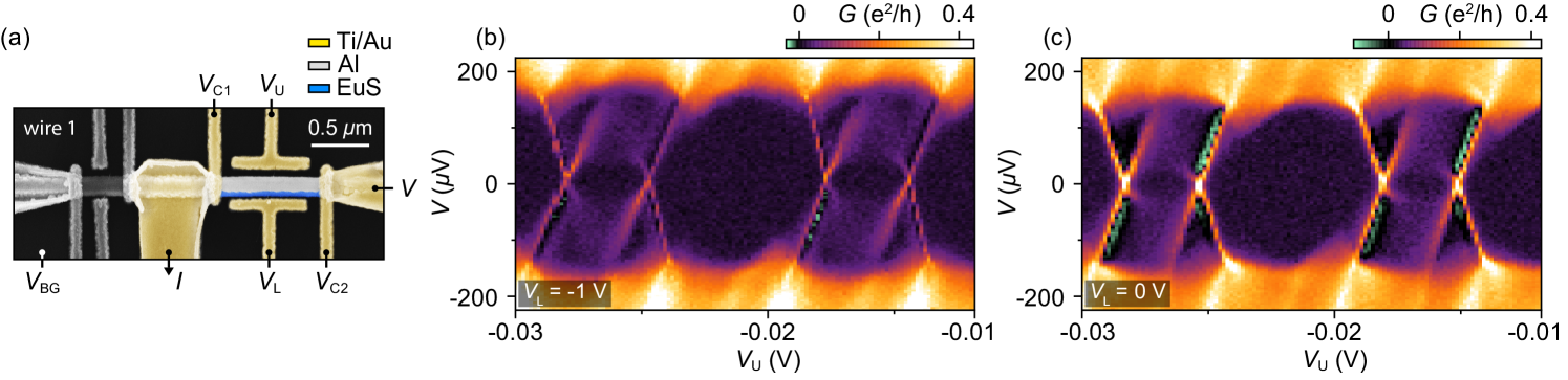
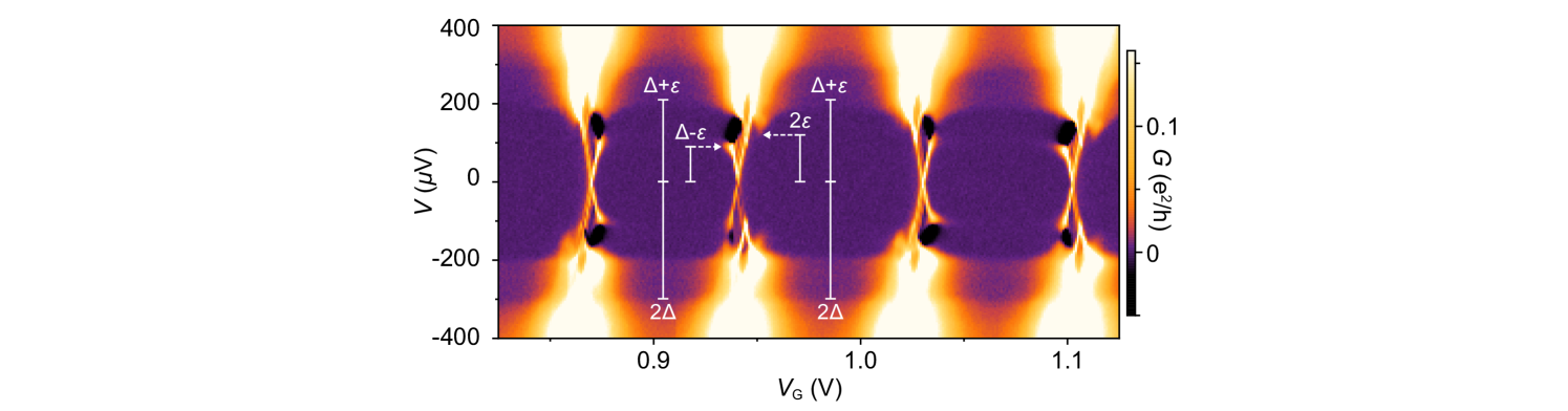
Differential conductance, , of the 400 nm island on wire 1 as a function of source-drain voltage bias, , and upper-gate voltage, , showed Coulomb diamonds of alternating height [Fig. 1(c)]. Once the tunneling barriers were coarsely tuned, this behavior is typical of all measured devices. Within a Coulomb valley, low-bias was suppressed below the experimental noise floor. At higher bias, showed a step-like increase at an alternating bias, as seen in Fig. 1(c). The value of at which this first-step feature occurs could be tuned using the lower-gate voltage, . A less pronounced second step in at higher bias [around V in Fig. 1(c)] did not alternate from valley to valley nor varied with (see Fig. S1 in Supplemental Material Sup ). The charging energy, eV, measured from the Coulomb diamonds, is larger than the superconducting gap of the parent Al shell, eV hence also larger than the induced gap, , which is reduced by the coupling to EuS Vaitiekėnas et al. (2021). The 800 nm island on wire 1 showed similar even-odd periodic Coulomb blockade with step-like cotunneling features at finite bias (see Fig. S2 in Supplemental Material Sup ).
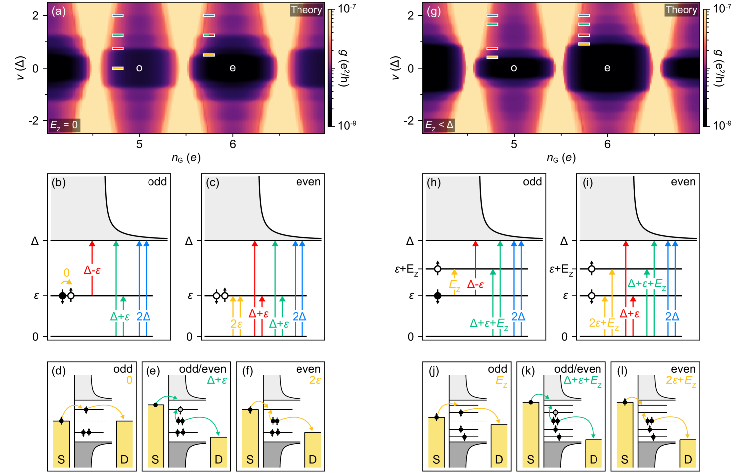
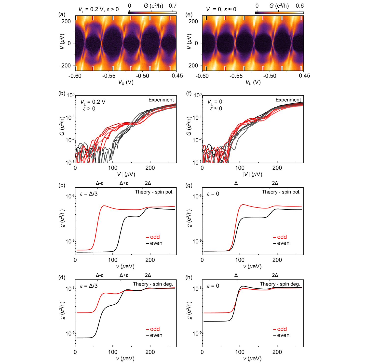
To understand the conductance features and relate them to ABSs and spin, we model transport through a superconducting Coulomb island, including a single subgap state, spin-split by Zeeman energy, . Sequential single-electron tunneling through an ABS on the island yields characteristic Coulomb diamonds Higginbotham et al. (2015); van Heck et al. (2016). To account for intermediate strengths of tunnel couplings to both leads we also include cotunneling processes Ekström et al. (2020) through a next-to-leading order expansion in the T-matrix (see Supplemental Material Sup ). Elastic cotunneling gives a bias independent background conductance, while inelastic cotunneling leaves the system in an excited state yielding steps in when the bias matches excitation energies.
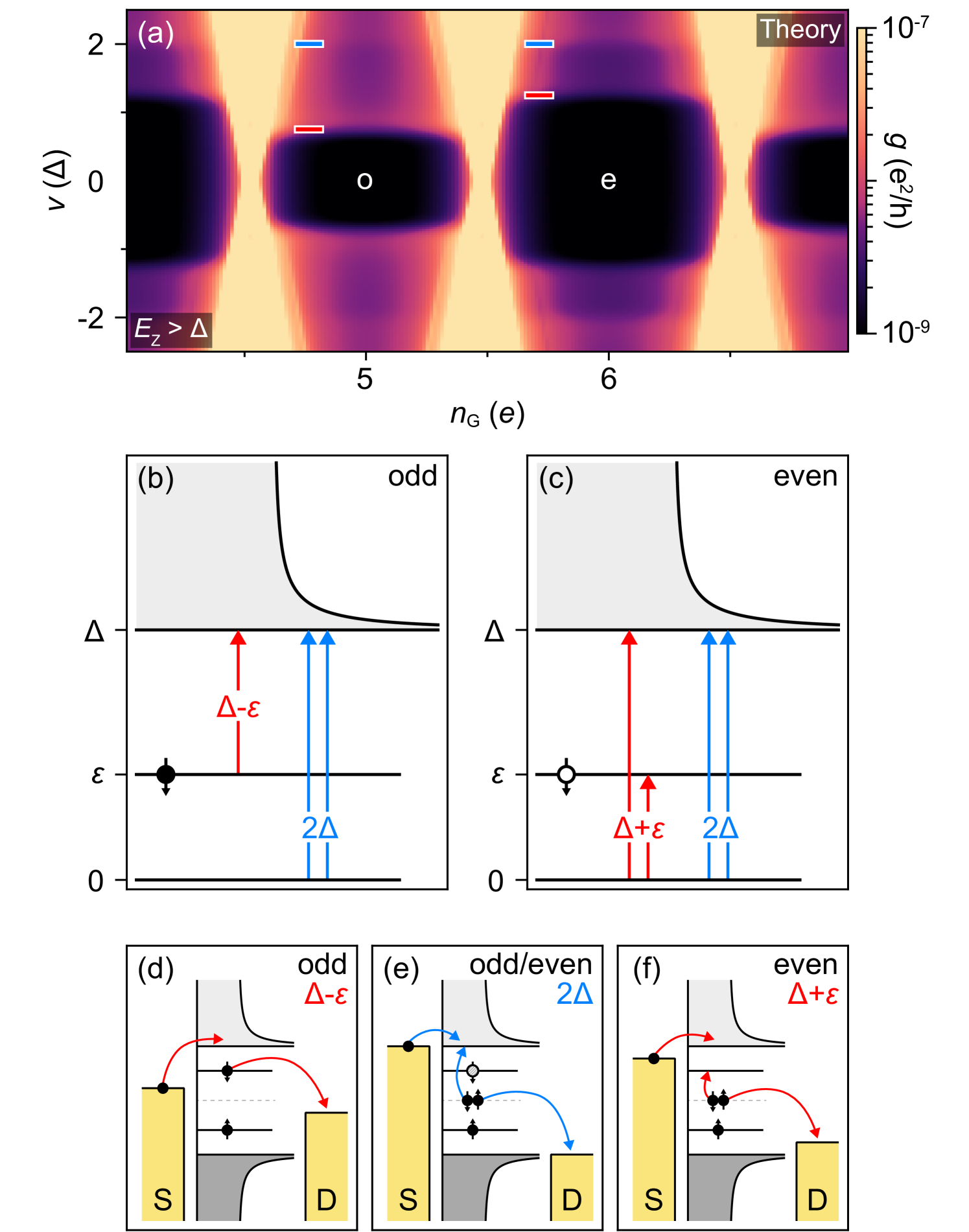
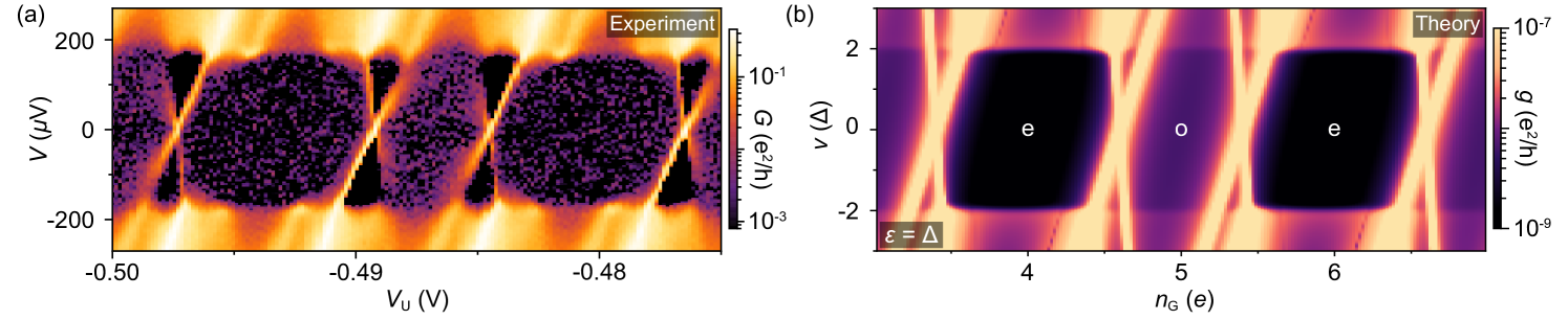
Theoretical values for differential conductance, , of a Coulomb island containing a single spin-split ABS as a function of voltage bias, , and gate-induced charge offset, , is shown in Fig. 2(a), where and are energies of the two spin branches. The main experimental features are captured qualitatively in this simple theoretical model. In particular, the bias value of the conductance step alternates between even (e) and odd (o) island parities. Steps in differential conductance, marked by the red and blue ticks, correspond to transitions between ground and lowest excited states, as illustrated in Figs. 2(b) and 2(c). Red lines marking for odd valleys and for even valleys correspond to processes that change the parity of the subgap state, while the blue lines marking for both valleys correspond to processes that break Cooper pairs without changing parity. Cotunneling processes involving higher-energy intermediate states with charge on the island are shown in Figs. 2(d)–2(f).
Theoretical spectra for spin-degenerate or weakly spin-split ABS show a denser pattern of cotunneling steps associated with excitations to spin-flipped states at fixed charge, as shown in Fig. S3 in Supplemental Material Sup . A qualitative comparison shows that the experimental data from Fig. 1(c) agree better with the spin-polarized rather than the spin-degenerate theory (see the discussion and Figs. S4 and S6 in Supplemental Material Sup ). Previous measurements of a similar hybrid island, but without the EuS shell, had shown Coulomb spectra that are consistent with the theory for a spin-degenerate bound state, see Fig. S7 in Supplemental Material Sup .
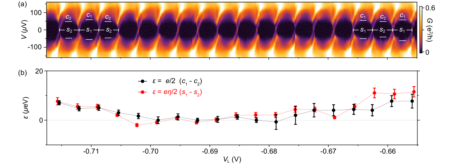
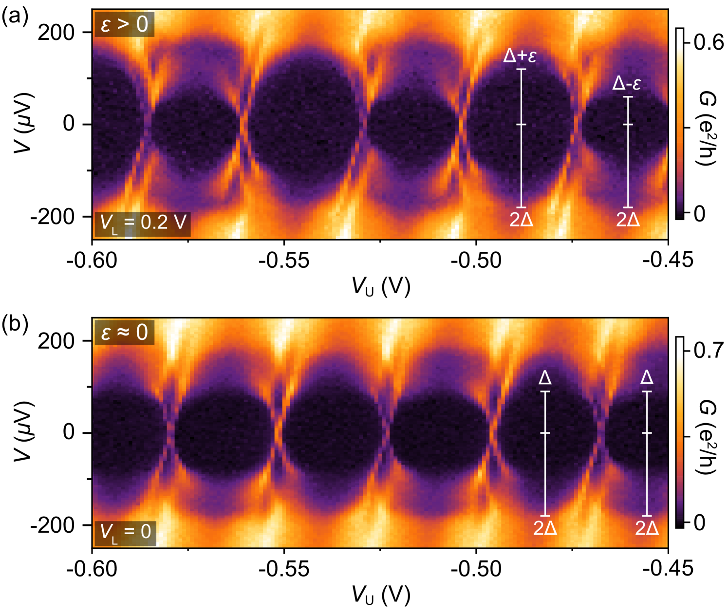
Returning to experiment, transport data for the 400 nm device on wire 2 shown in Fig. 1(c) yield eV and eV, giving eV and eV, consitent with the feature at eV. The data in Fig. 1(c) gives a slightly smaller eV. We note that can be gate-voltage dependent. In general, the induced gap is considerably smaller than the parent Al gap in these wires. The deduced eV is larger than , consistent with the even-odd periodic Coulomb pattern. The sharp spectral features at the degeneracy points indicate a discrete subgap state.
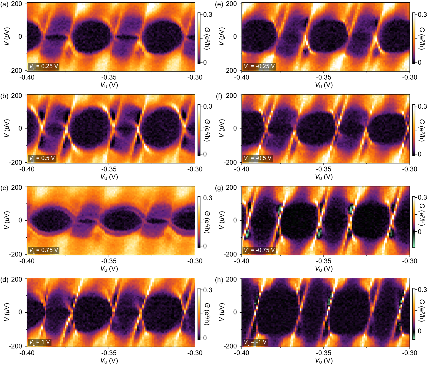
Decreasing from +0.2 V to 0 modifies the Coulomb blockade peaks from distinctly even-odd to -periodic at zero bias, with consecutive diamonds differing only by the intensity of step features at finite bias, as seen in Fig. 3(b). The onsets of the lower-energy steps in both valleys align with eV, indicating that .
We interpret the evolution as reflecting a subgap state that gradually decreases to zero energy as is varied. In other words, the gate-induced electric fields change the electrostatic environment of the hybrid nanowire, thus modifying the parameters of the subgap state and effectively changing its energy. In the present context, the evolving spin-mixing angle at the superconductor-ferromagnetic insulator interface Hübler et al. (2012) contributes to the gate dependence of .
Similar measurements at various are shown in Fig. S8 in Supplemental Material Sup . The even-odd structure in the amplitude of the finite bias conductance steps is expected theoretically, and reflects the relative phase difference between electron and hole components of the subgap state (see the discussion and Fig. S9 in Supplemental Material Sup ).
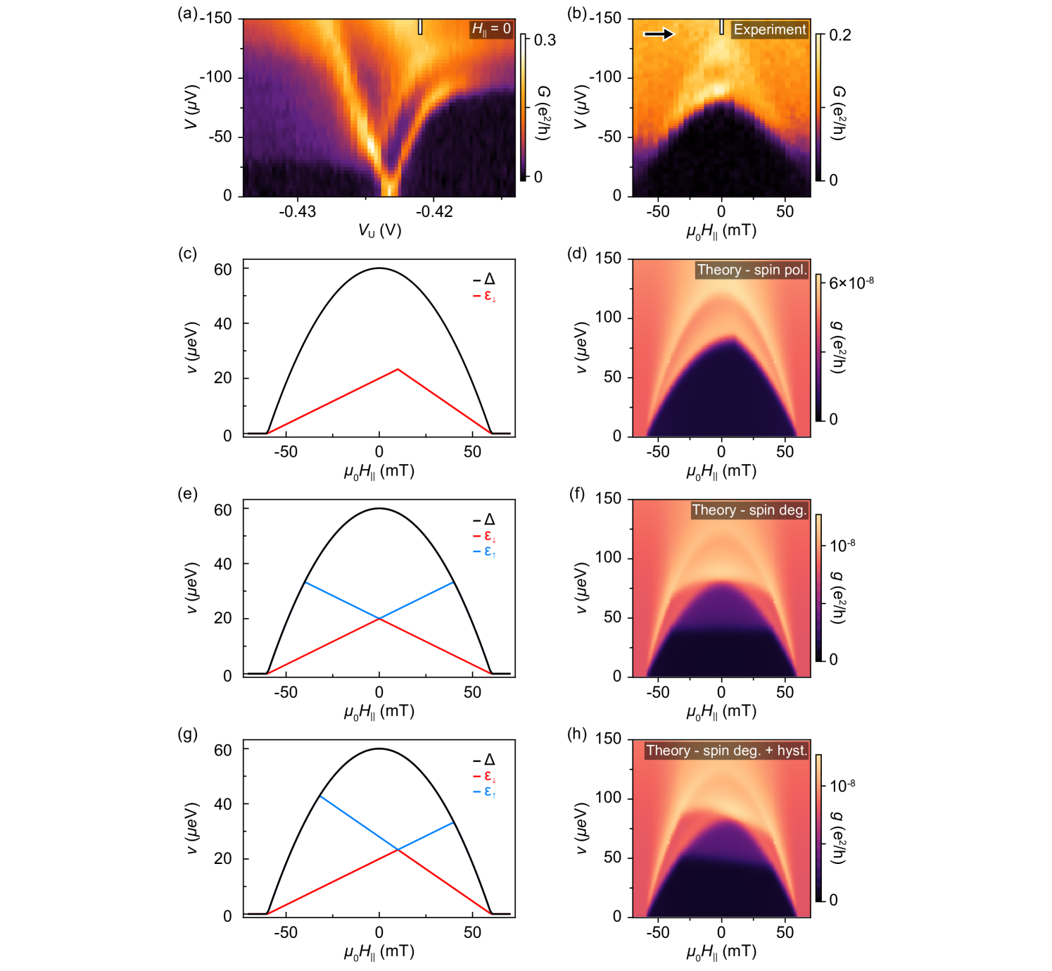
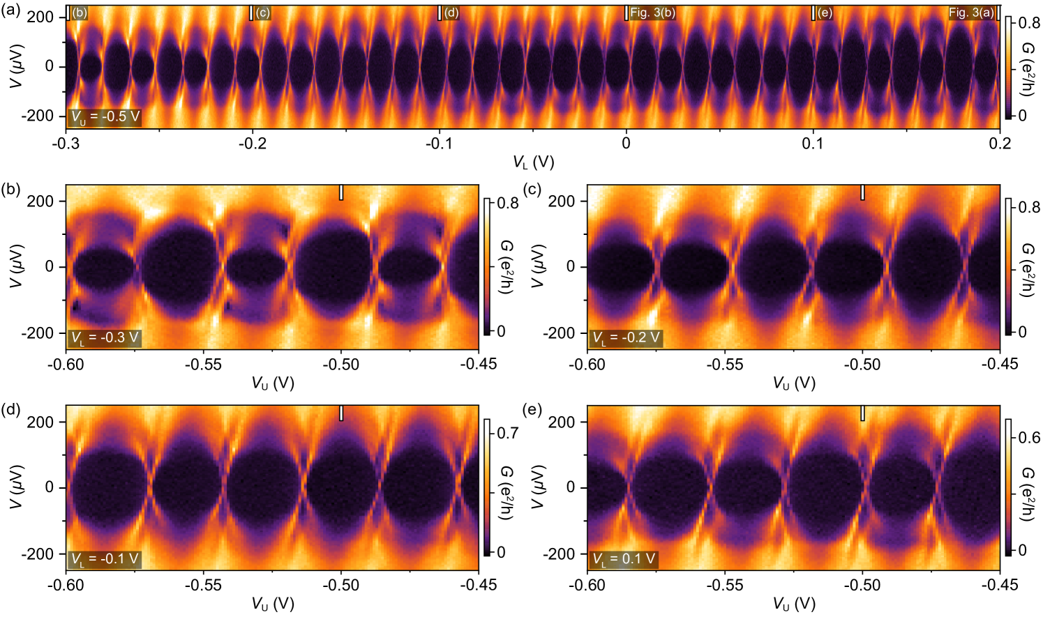
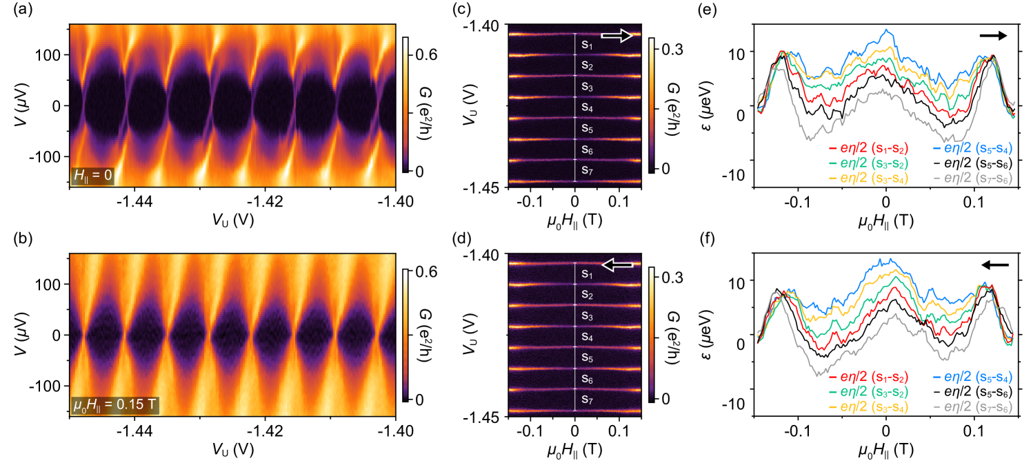
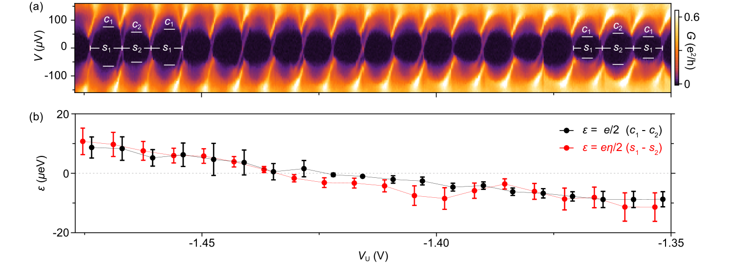
To investigate dependence on the electrostatic environment we look over a wider range of gate voltages. The observed even-odd pattern crosses smoothly through 1 periodicity, reflecting the continuous evolution of across zero. This is shown in Fig. 4(a) as a function of upper-gate voltage, , for the 800 nm island on wire 2. Both the onsets of the high-bias features, at values , and the peak spacings, , alternate in magnitude. Subscripts and 2 denote the two different charge occupancies of the island. We define and , then take the difference between consecutive to extract the subgap-state energy , as a function of as shown in Fig. 4(b). Within the measured range of , decreases monotonically from eV to eV. Independently, values for were extracted from Coulomb peak spacing at zero bias Higginbotham et al. (2015); Albrecht et al. (2016); Shen et al. (2018). For , peak spacings are given by and , where is a dimensionless lever arm measured from the slopes of the Coulomb diamonds. The subgap-state energy inferred from the Coulomb peak spacing difference agrees well with deduced from finite bias steps, as shown in Fig. 4(b). Good qualitative agreement between measured and computed spectra is shown in Fig. S10 in Supplemental Material Sup . Similar analysis for as a function of , where the subgap state approaches but does not cross zero energy, is shown in Fig. S11 in Supplemental Material Sup .
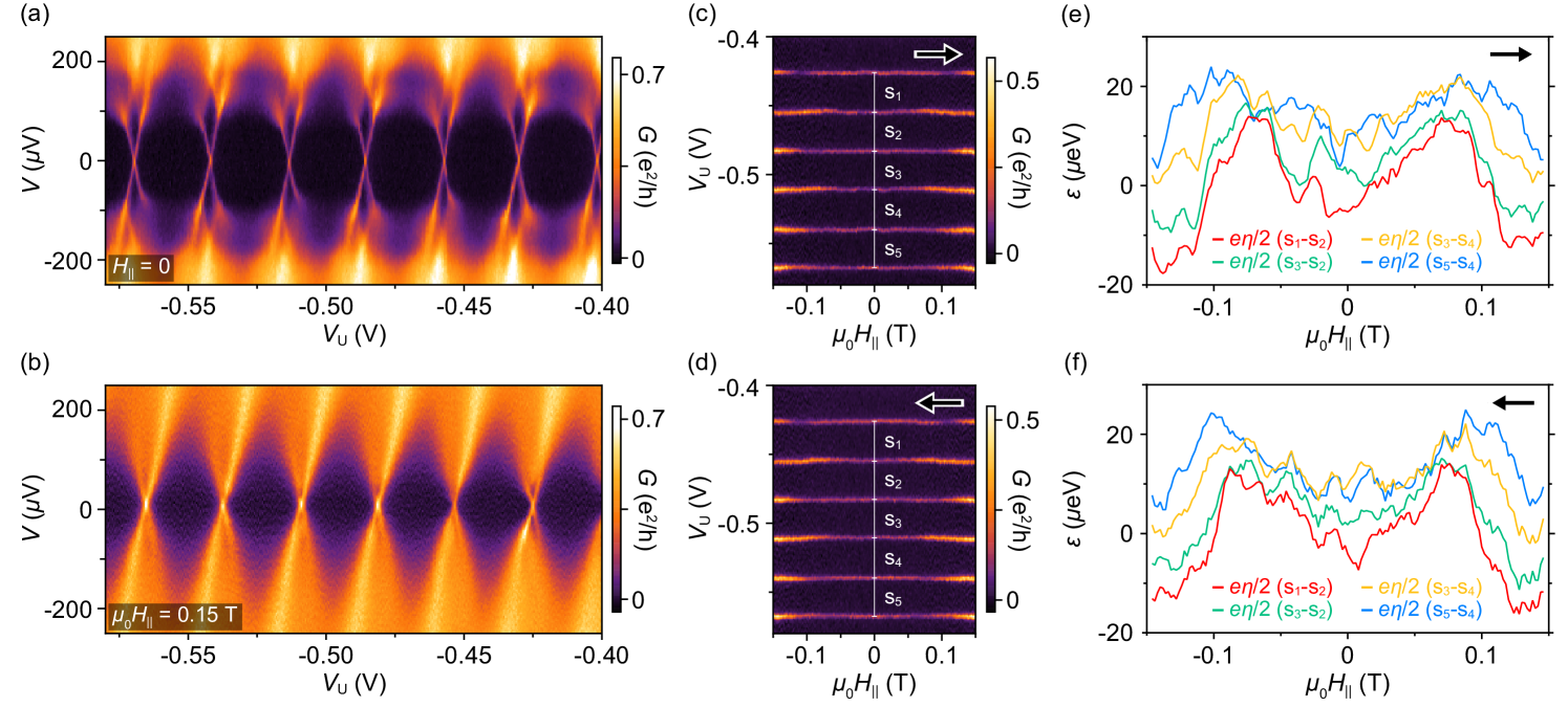
The sign of depends on the definition of and . Assuming strong zero-field spin splitting at zero applied magnetic field leaves it ambiguous whether or not a level has crossed zero energy. We therefore cannot label the even and odd valleys with certainty. We note that while in principle the evolution of with applied magnetic field contains information on the spin projection of the bound state and hence the ground state parity, we are not able to determine if the field predominantly affects the Zeeman splitting or the magnetization of the EuS (see Ref. Vaitiekėnas et al. (2021)). Representative magnetic-field data for both islands on wire 2 are shown in Figs. S11 and S12 in Supplemental Material Sup .
Finally, we note that for specific gate configurations there are no inelastic cotunneling steps present in Coulomb diamonds (see Fig. S14 in Supplemental Material Sup ). This can be understood within the model as resulting from the condition , yielding a cotunneling background for all voltage-bias values within odd valleys and non-zero conductance above in even valleys.
We thank Claus Sørensen for contributions to materials growth and Shivendra Upadhyay for assistance with nanofabrication. We acknowledge support from the Danish National Research Foundation, European Research Council (Grants Agreement No. 716655 and No. 856526), Microsoft, NanoLund, QuantERA (Project ”2D hybrid materials as a platform for topological quantum computing”), and a research grant (Project 43951) from VILLUM FONDEN.
References
- Meservey and Tedrow (1994) R. Meservey and P. Tedrow, Phys. Rep. 238, 173 (1994).
- Buzdin (2005) A. I. Buzdin, Rev. Mod. Phys. 77, 935 (2005).
- Sau et al. (2010) J. D. Sau, R. M. Lutchyn, S. Tewari, and S. Das Sarma, Phys. Rev. Lett. 104, 040502 (2010).
- Eschrig (2011) M. Eschrig, Phys. Today 64, 43 (2011).
- Li et al. (2014) J. Li, H. Chen, I. K. Drozdov, A. Yazdani, B. A. Bernevig, and A. MacDonald, Phys. Rev. B 90, 235433 (2014).
- Linder and Robinson (2015) J. Linder and J. W. Robinson, Nat. Phys. 11, 307 (2015).
- Strambini et al. (2017) E. Strambini, V. Golovach, G. De Simoni, J. Moodera, F. Bergeret, and F. Giazotto, Phys. Rev. Mater. 1, 054402 (2017).
- Bergeret et al. (2018) F. S. Bergeret, M. Silaev, P. Virtanen, and T. T. Heikkilä, Rev. Mod. Phys. 90, 041001 (2018).
- Manna et al. (2020) S. Manna, P. Wei, Y. Xie, K. T. Law, P. A. Lee, and J. S. Moodera, PNAS 117, 8775 (2020).
- Vaitiekėnas et al. (2021) S. Vaitiekėnas, Y. Liu, P. Krogstrup, and C. Marcus, Nat. Phys. 17, 43 (2021).
- Higginbotham et al. (2015) A. P. Higginbotham, S. M. Albrecht, G. Kiršanskas, W. Chang, F. Kuemmeth, P. Krogstrup, T. S. Jespersen, J. Nygård, K. Flensberg, and C. M. Marcus, Nat. Phys. 11, 1017 (2015).
- Prada et al. (2020) E. Prada, P. San-Jose, M. W. de Moor, A. Geresdi, E. J. Lee, J. Klinovaja, D. Loss, J. Nygård, R. Aguado, and L. P. Kouwenhoven, Nat. Rev. Phys. 2, 575 (2020).
- Pillet et al. (2010) J. Pillet, C. Quay, P. Morfin, C. Bena, A. L. Yeyati, and P. Joyez, Nat. Phys. 6, 965 (2010).
- Nichele et al. (2020) F. Nichele, E. Portolés, A. Fornieri, A. Whiticar, A. Drachmann, S. Gronin, T. Wang, G. Gardner, C. Thomas, A. Hatke, M. Manfra, and C. Marcus, Phys. Rev. Lett. 124, 226801 (2020).
- Grove-Rasmussen et al. (2009) K. Grove-Rasmussen, H. I. Jørgensen, B. M. Andersen, J. Paaske, T. S. Jespersen, J. Nygård, K. Flensberg, and P. E. Lindelof, Phys. Rev. B 79, 134518 (2009).
- Chang et al. (2013) W. Chang, V. E. Manucharyan, T. S. Jespersen, J. Nygård, and C. M. Marcus, Phys. Rev. Lett. 110, 217005 (2013).
- van Dam et al. (2006) J. A. van Dam, Y. V. Nazarov, E. P. Bakkers, S. De Franceschi, and L. P. Kouwenhoven, Nature 442, 667 (2006).
- Jørgensen et al. (2007) H. I. Jørgensen, T. Novotnỳ, K. Grove-Rasmussen, K. Flensberg, and P. Lindelof, Nano Lett. 7, 2441 (2007).
- Lee et al. (2014) E. J. Lee, X. Jiang, M. Houzet, R. Aguado, C. M. Lieber, and S. De Franceschi, Nat. Nanotechnol. 9, 79 (2014).
- Shen et al. (2018) J. Shen, S. Heedt, F. Borsoi, B. van Heck, S. Gazibegovic, R. L. O. het Veld, D. Car, J. A. Logan, M. Pendharkar, S. J. Ramakers, et al., Nat. Comm. 9, 1 (2018).
- Heinrich et al. (2018) B. W. Heinrich, J. I. Pascual, and K. J. Franke, Prog. Surf. Sci. 93, 1 (2018).
- Whiticar et al. (2021) A. Whiticar, A. Fornieri, A. Banerjee, A. Drachmann, S. Gronin, G. Gardner, T. Lindemann, M. Manfra, and C. Marcus, arXiv:2101.09706 (2021).
- Hays et al. (2020) M. Hays, V. Fatemi, K. Serniak, D. Bouman, S. Diamond, G. de Lange, P. Krogstrup, J. Nygård, A. Geresdi, and M. Devoret, Nat. Phys. 16, 1103 (2020).
- Tokuyasu et al. (1988) T. Tokuyasu, J. A. Sauls, and D. Rainer, Phys. Rev. B 38, 8823 (1988).
- Hübler et al. (2012) F. Hübler, M. Wolf, T. Scherer, D. Wang, D. Beckmann, and H. v. Löhneysen, Phys. Rev. Lett. 109, 087004 (2012).
- Diesch et al. (2018) S. Diesch, P. Machon, M. Wolz, C. Sürgers, D. Beckmann, W. Belzig, and E. Scheer, Nat. Commun. 9, 5248 (2018).
- Krogstrup et al. (2015) P. Krogstrup, N. Ziino, W. Chang, S. Albrecht, M. Madsen, E. Johnson, J. Nygård, C. Marcus, and T. Jespersen, Nat. Mater. 14, 400 (2015).
- Liu et al. (2020a) Y. Liu, S. Vaitiekėnas, S. Marti-Sanchez, C. Koch, S. Hart, Z. Cui, T. Kanne, S. A. Khan, R. Tanta, S. Upadhyay, M. Espineira Cachaza, C. M. Marcus, J. Arbiol, K. A. Moler, and P. Krogstrup, Nano Lett. 20, 456 (2020a).
- Woods and Stanescu (2020) B. D. Woods and T. D. Stanescu, arXiv:2011.01933 (2020).
- Maiani et al. (2021) A. Maiani, R. S. Souto, M. Leijnse, and K. Flensberg, Phys. Rev. B 103, 104508 (2021).
- Escribano et al. (2020) S. Escribano, E. Prada, Y. Oreg, and A. Levy Yeyati, arXiv:2011.06566 (2020).
- Liu et al. (2020b) C.-X. Liu, S. Schuwalow, Y. Liu, K. Vilkelis, A. Manesco, P. Krogstrup, and M. Wimmer, arXiv:2011.06567 (2020b).
- Langbehn et al. (2021) J. Langbehn, S. A. González, P. W. Brouwer, and F. von Oppen, Phys. Rev. B 103, 165301 (2021).
- Khindanov et al. (2021) A. Khindanov, J. Alicea, P. Lee, W. S. Cole, and A. E. Antipov, Phys. Rev. B 103, 134506 (2021).
- (35) See Supplemental Material for more detailed methods and simulation description, as well as additional measurements.
- van Heck et al. (2016) B. van Heck, R. M. Lutchyn, and L. I. Glazman, Phys. Rev. B 93, 235431 (2016).
- Ekström et al. (2020) J. Ekström, P. Recher, and T. L. Schmidt, Phys. Rev. B 101, 195420 (2020).
- Albrecht et al. (2016) S. M. Albrecht, A. P. Higginbotham, M. Madsen, F. Kuemmeth, T. S. Jespersen, J. Nygård, P. Krogstrup, and C. M. Marcus, Nature 531, 206 (2016).
- Liu et al. (2020c) Y. Liu, A. Luchini, S. Martí-Sánchez, C. Koch, S. Schuwalow, S. A. Khan, T. Stankevič, S. Francoual, J. R. Mardegan, J. Krieger, V. N. Strocov, J. Stahn, C. A. F. Vaz, M. Ramakrishnan, U. Staub, K. Lefmann, G. Aeppli, J. Arbiol, and P. Krogstrup, ACS Appl. Mater. Interfaces 12, 8780 (2020c).
- Grove-Rasmussen et al. (2018) K. Grove-Rasmussen, G. Steffensen, A. Jellinggaard, M. H. Madsen, R. Žitko, J. Paaske, and J. Nygård, Nat. Comm. 9, 2376 (2018).
- Bruus and Flensberg (2004) H. Bruus and K. Flensberg, Many-body quantum theory in condensed matter physics: an introduction (Oxford university press, 2004).
- Koller et al. (2010) S. Koller, M. Grifoni, M. Leijnse, and M. R. Wegewijs, Phys. Rev. B 82, 235307 (2010).
- Koch et al. (2004) J. Koch, F. von Oppen, Y. Oreg, and E. Sela, Phys. Rev. B 70, 195107 (2004).
- Ozaki (2007) T. Ozaki, Phys. Rev. B 75, 035123 (2007).
I Supplemental Material
II Sample preparation
InAs wires with hexagonal cross section were grown to a length of m and diameter of nm using molecular beam epitaxy Krogstrup et al. (2015). Partly-overlapping, two-faceted EuS (as grown thickness 8 nm) and Al (as grown thickness 6 nm) shells were grown in situ using electron beam evaporation, as shown in the main-text Fig. 1(a) Liu et al. (2020c, a). Devices were fabricated on a Si substrate with 200 nm SiOx capping. Coulomb islands were formed by wet-etching (MF-321 photoresist developer, 30 s, room temperature) and contacting the exposed InAs/EuS with Ti/Au (5/150 nm) after in situ Ar milling (15 W, 7 min). Devices were then coated with a HfO2 (8 nm) dielectric layer, followed by the deposition of Ti/Au (5/150 nm) gates patterned using electron beam lithography. Additional details can be found in Ref. Vaitiekėnas et al. (2021).
III Measurements
The samples were cooled to base temperature of the dilution refrigerator at zero applied magnetic field. Following cooldown, an external magnetic field was applied mT along the wire axis then returned to zero. Unless otherwise noted, the measurements were carried out at zero applied field. Differential conductance, dd, was measured by sourcing voltage bias, , through one of the outer leads, floating the opposite end of the wire, and draining the current, , through the common lead between the two islands, as shown for the 400 nm island in the main-text Fig. 1(b) and for the 800 nm island in Fig. S2(a). The islands were tuned into the Coulomb blockade regime using negative voltages applied to the cutter gates, and , and back gate, [labeled only in Fig. S2(a)]. Over a range much larger than the Coulomb peak spacing, also tuned the chemical potential of the island. The upper-gate voltage, , on the side coated with the Al shell, was predominantly used to tune the occupancy of the hybrid island, whereas the lower-gate voltage, , on the EuS shell side, was used to tune the charge carrier density in the semiconductor.
IV Model
We consider a superconducting island hosting a subgap state that can be spin-slit (for example, due to exchange-coupling to the ferromagnetic insulator) by an energy . For simplicity, we describe the continuum of states as a spin-degenerate quasiparticle state at energy , using the so-called zero bandwidth model Grove-Rasmussen et al. (2018). We take the charging energy of the island, , to be the largest and the coupling to the leads to be the smallest energy scales in the system, allowing us to treat the electron tunneling in a perturbative way.
The Hamiltonian of the system is given by
| (1) |
where the leads are described by
| (2) |
with the energy, , and the annihilation operator, , of an electron in lead with momentum and spin . We assume that each lead remains in internal equilibrium described by a Fermi-Dirac distribution with chemical potential .
The superconducting island is described by
| (3) |
where is the state index, is the (spin-dependent) energy of subgap and continuum states, is the Bogoliubov quasiparticle annihilation operator, and is the electrostatic repulsion term that depends on the number of electrons in the island, , where is the number of Cooper pairs and is the total charge in the quasiparticle states. For the subgap state, we take and . For simplicity, we take spin-degenerate continuum states at . Similar results are found for spin-split continuum states. The annihilation operator for an electron in the island, , is related to by
| (4) |
where and are the Bogoliubov coefficients, depending on the spin, is the superconducting phase operator such that creates a Cooper pair on the island, and is the spin opposite to . The electrostatic repulsion term is given by
| (5) |
where is the dimensionless gate-induced charge offset.
The tunneling Hamiltonian is described by
| (6) |
where denotes the tunneling amplitudes between the island and leads.
V Formalism
The transport properties through the superconducting island are calculated using the T-matrix formalism Bruus and Flensberg (2004). The transition rate between initial, , and final, , states can be computed by
| (7) |
where weights the rate through thermal distributions of initial and final states at energies and , respectively, is the Dirac delta function and
| (8) |
which can be truncated at the desired order. Here the term linear in describes the sequential tunneling; the higher order terms describe the cotunneling contributions, which become progressively more important when the tunneling coupling between the island and the leads increases.
The quantum state of the island is described by =, where n is a vector representing the occupation of the subgap and continuum excited states. The time derivative of the occupation probability of a given state can be written as
| (9) |
which describes the stationary probability of occupation, , by imposing and . The current through the device can be computed using the stationary distribution of probabilities and the rates. The tunneling current is given by
| (10) |
where for rightwards sequential tunneling and for the opposite direction, is the net charge transferred from left to right in a cotunneling process, and the sum runs over all the possible rates connecting the island state with any state .
VI Sequential tunneling rates
The sequential rates are given by
| (11) | ||||
where is the Fermi-Dirac distribution function and is the chemical potential of the lead . Here, we have used the wideband approximation, where the tunneling rates are energy independent and , with the lead density of states at the Fermi level . Note that for these rates n and differ by the occupation of one state.
VII Cotunneling rates
We consider the cotunneling rates transferring an electron from one lead to the other, which are the dominant ones in the limit , where is the source-drain voltage bias used in calculations. These processes, which conserve the charge on the island, can be expressed by
| (12) |
where describes the tunneling between lead and the island, denotes a lead opposite to , and are virtual intermediate states. To derive this expression we have imposed energy conservation, which leads to a function dependent on the energy of the tunneling electron from/to one of the leads, . The cotunneling rate can be written as
| (13) |
This expression for the cotunneling rates is divergent due to the appearing sequential tunneling. To avoid the divergent behaviour, we regularize the divergences as explained in Ref. Koller et al. (2010). The resulting integral can be formally solved analytically Koch et al. (2004), which leads to a complicated expression involving special functions. In the limit of , it turns out to be more computationally efficient to simplify it by expanding into a sum of complex Matsubara-Ozaki frequencies Ozaki (2007)
| (14) |
where and are the approximated Matsubara frequencies and residues, respectively. Finally, Eq. (13) can be evaluated using the residue theorem yielding
| (15) |
This sum can be truncated at Matsubara frequencies for the parameters used in the calculations.
VIII Transport calculations
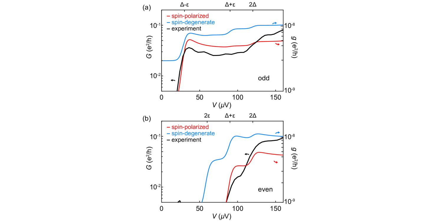
Calculated Coulomb spectra for a spin-degenerate () and weakly spin-split () subgap states are shown in Figs. S3(a) and S3(g). The colored ticks mark the onset of inelastic cotunneling events that excite the system into a higher-energy state, resulting in a step-like increase in conductance. The transitions in the odd and even valleys are represented separately in panels (b) and (c) for the spin-degenerate, and panels (h) and (i) for the weakly spin-split cases. Some examples of the cotunneling transport mechanisms for the two cases are illustrated in panels (d)–(f) and (j)–(l), respectively. In general, there are four cotunneling lines in both spin-degenerate and weakly spin-split cases (except for the specific instances where is fine tuned such that two transitions are degenerate in energy). In contrast, our experimental data show only two cotunneling steps (see, for example, Fig. 3 in the main text). A qualitative line-cut comparison between experimental data and spin-polarized as well as spin-degenerate cases is shown for the 400 nm island on wire 1 in Fig. S4. Aggregated line-cuts from several consecutive even and odd Coulomb valleys measured for the 400 nm island on wire 2 display two cotunneling steps, independent of lower-gate voltage and subgap-state energy, see Fig. S5.
The measured cotunneling features decrease in energy without splitting as an external magnetic field is applied, see Fig. S6(b). For comparison, we calculate conductance for a spin-polarized and two spin-degenerate cases—with and without magnetic hysteresis. As an input, we use approximated expressions for the field dependence of the superconducting gap and the subgap states. We describe the gap closing as , with critical field mT and the zero-field gap eV, see the black curves in Fig. S6(c), (e), and (g). For simplicity we assume that the subgap state depends linearly on the field, see the red and blue curves in Fig. S6(c), (e), and (g). To account for the asymmetry in the measured data, we include magnetic hysteresis of 10 mT (consistent with previous experiments Vaitiekėnas et al. (2021)) in the spin-polarized and one of the spin-degenerate cases. The magnetic field in the spin-degenerate case leads to the appearance of additional cotunneling features that are not observed experimentally, see Fig. S6(f) and (h). We therefore find that the measurements agree best with the spin-polarized spectrum shown in Fig. S6(d).
We note that the number of cotunneling steps increases in similar hybrid island devices without EuS shell (see the replotted data from Ref. Higginbotham et al. (2015) in Fig. S7) consistent with Fig. S3(a).
These observations together suggest that the investigated hybrid islands are in the strongly spin-split limit (), discussed in the main-text Fig. 2.
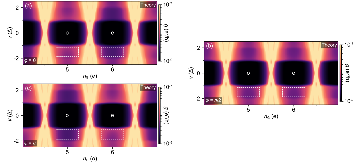
The relative height of the cotunneling steps in the even and odd Coulomb valleys depends on the relative phase, , between the Bogoliubov components of the subgap state, and , as illustrated in Fig. S9 for and . The effect can be explained by the interference between different cotunneling mechanisms that involve the same initial and final states. However, cannot be determined unambiguously in our setup, as the strong spin splitting and gate-dependent makes the global ground state unknown. This remains an open problem, relevant for distinguishing trivial and topological states.
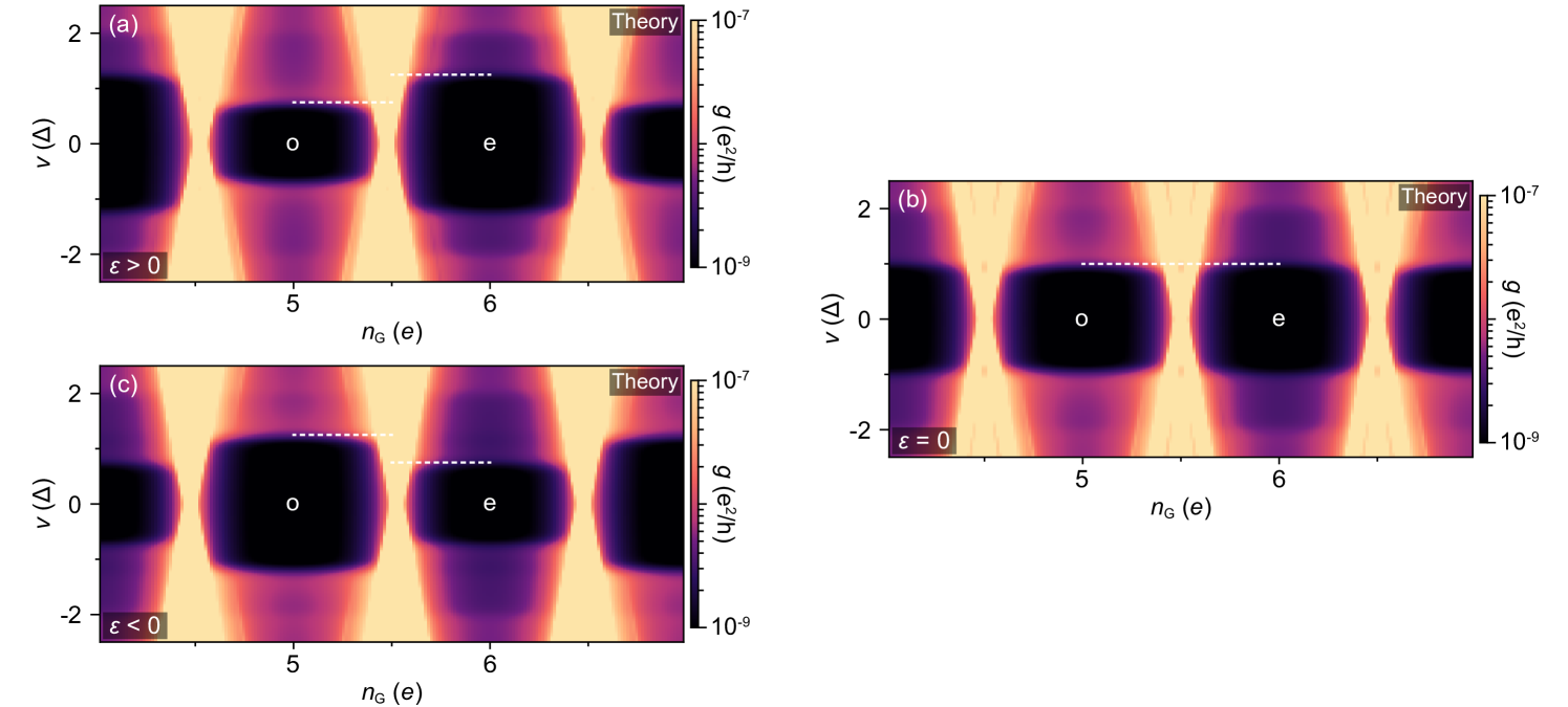
In the experiment, the magnitude and, in some cases, the sign of can be tuned using electrostatic gate electrodes (Fig. 4 in the main text). In our model, we account for this behavior by changing in Eq. (3). A change in the sign of is equivalent to exchanging the Bogoliubov components of the corresponding subgap state. In Fig. S10 we show the calculated conductance in the strongly spin-split case for greater than, equal to, and less than zero. For , the Coulomb blockade is 1-periodic—the onsets of the lowest cotunneling steps in both odd and even valleys align at . For away from zero, the spectrum is even-odd periodic with the inelastic onset at in the odd and in the even valleys. The sign of determines the relative size of odd and even Coulomb diamonds.