Field-Effect Josephson Diode
via Asymmetric Spin-Momentum-Locking States
Abstract
Recent breakthroughs in Josephson diodes dangle the possibility of extending conventional non-reciprocal electronics into the realm of superconductivity. While a strong magnetic field is recognized for enhancing diode efficiency, it concurrently poses a risk of undermining the essential superconductivity required for non-dissipative devices. To circumvent the need for magnetic-based tuning, we propose a field-effect Josephson diode based on the electrostatic gate control of finite momentum Cooper pairs in asymmetric spin-momentum-locking states. We propose two possible implementations of our gate-controlled mechanism: (i) a topological field-effect Josephson diode in time-reversal-broken quantum spin Hall insulators; and (ii) semiconductor-based field-effect Josephson diodes attainable in current experimental setups involving a Zeeman field and spin-orbit coupling. Notably, the diode efficiency is highly enhanced in the topological field-effect Josephson diode because the current carried by the asymmetric helical edge states is topologically protected and can be tuned by local gates. In the proposed Josephson diode, the combination of gates and asymmetric spin-momentum-locking nature is equivalent to that of a magnetic field, thus providing an alternative electrical operation in designing nonreciprocal superconducting devices.
I Introduction
Electronic technologies rely heavily on non-reciprocal charge-transport semiconducting devices such as diodes, alternating-to-direct current converters, and transistors [1, 2, 3, 4]. However, dissipation is inevitable in such devices due to their finite resistance [5]. Superconducting (SC) diodes [6, 7] in noncentrosymmetric superconductor [8, 9, 10, 11, 12, 13, 14, 15, 16, 17, 19, 21, 18, 20] and Josephson junctions [22, 23, 24, 26, 27, 25, 28, 29, 39, 36, 38, 32, 33, 40, 31, 30, 37, 35, 34] are promising dissipationless non-reciprocal devices that manifest in direction-selective critical supercurrents, i.e. where is the critical supercurrent in positive/negative direction. When an external applied current lies between and , the transport is dissipationless in one direction due to Cooper-pair formation, while dissipative in the opposite direction due to the destruction of Cooper pairs [Fig. 1(a)].
The extent of non-reciprocity is characterized by the diode efficiency,
| (1) |
and defines the diode polarity. Numerous theoretical findings [41, 42, 43, 44, 45, 46, 47, 48, 50, 49, 51, 52, 53, 54, 55, 68, 57, 58, 59, 60, 61, 62, 67, 63, 64, 65, 66, 68, 71, 69, 56, 73, 74, 72, 70] in topological insulators [50, 51, 67, 66, 68, 69, 70], half-metallic trilayers [54], supercurrent interferometers [61, 62] and, semiconductors subjected to the interplay with spin-orbit interactions (SOIs) and Zeeman field [71, 72] have suggested SC diodes as potential building blocks for high-performance SC circuits.
Simultaneously breaking inversion and time-reversal symmetry (TRS) is necessary for SC diode effect [75, 76, 77]. A resulting additional unidirectional supercurrent is induced causing the non-reciprocity [60, 78, 79, 80]. To break inversion symmetry, a nuanced device design is essential where the diode efficiency is sensitive to structural parameters [21], and challenging to tune once a device is fabricated. Thus, in most experiments, SC diode effects are activated and manipulated by external magnetic fields, a typical method for breaking TRS. Unfortunately, superconductivity will ultimately be impaired by sufficiently high magnetic fields, thereby fundamentally limiting their applications [81]. Attention then is drawn to magnetic-field-free SC diodes [19, 20, 21, 36, 37, 39, 38, 40], where TRS is broken by intrinsic magnetism. However, external magnetic fields are still necessary for diode-on/off and polarity-switching [39]. As such, an all-electrically-controlled SC diode is still under demand, which enhances the flexibility in operating integrated SC circuits.
This work proposes a new mechanism for an all-electrically-controlled Josephson diode, wherein supercurrents are carried by asymmetric spin-momentum-locking states (ASMLSs) characterized by electrons with opposite spins counter-propagating with different velocities (Fig. 1). Specifically, we show that the combination of asymmetry and gate voltage in the SC leads plays an equivalent role as a magnetic field to control the center-of-mass velocity of paired electrons, which leads to a unidirectional supercurrent. This enables the construction of an all-electrically controllable Josephson diode circumventing magnetic control. Hence, the proposed device can be termed as a field-effect Josephson diode (FEJD).
A proof-of-concept FEJD is proposed in a specific type of TRS-broken quantum spin Hall insulator (QSHI) with asymmetric helical edge states, which is predicted in Floquet topological insulator [82] and magnetic-doped QSHI with a small magnetic field [84, 83] such as HgTe [80, 22] and MnBi2Te4 [85, 86]. Since the supercurrents carried by the asymmetric helical edge states are topologically protected [87, 88, 89, 90, 91, 92, 93, 94], resembling the topological Josephson junction [89], the resulting device can be dubbed as topological FEJD.
The mechanism of realizing a FEJD using ASMLSs is also attainable in semiconductors which are widely investigated in recent experiments [39, 28, 29, 30, 27, 26, 40]. With the interplay between spin-orbit interaction (SOI) and in-plane Zeeman fields, electrons near the Fermi surface of the sample are described by ASMLSs. Our mechanism attributing the gate-tunable behavior to the ASMLSs provides an alternative theoretical explanation on a recent experiment [40].
The remainder of this work is organized as follows. The properties of ASMLSs and the mechanism of FEJD induced by ASMLSs are introduced in Sec. II. The mechanism is schematically demonstrated in Fig. 1, where the gate-tunable center-of-mass momentum of paired electrons and the Doppler energy shift play critical roles. The conceptual FEJD is specialized in two scenarios: topological FEJD in QSHI with asymmetric helical edge states (Sec. III) and semiconducting systems subjected to the interplay between SOIs and Zeeman fields (Sec. IV). The results are supported by the details involving scattering matrix formalism and tight-binding model simulation in the appendix A-E. Conclusions and discussions on experimental realization and the universality of ASMLS are given in Sec. V.
II General behavior of field-effect Josepshon diode
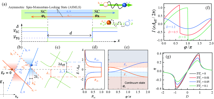
The mechanism of FEJD induced by ASMLSs is demonstrated in this section schematized in Fig. 1. The general properties of ASMLS are introduced in Sec. II.1, including its characteristics and potential implementation to the gate-tunable center-of-mass momentum of paired electrons when SC pairing is considered. The general transport properties of FEJD are demonstrated in Sec. II.2 including the asymmetric Andreev reflection probabilities, Andreev bound states (ABSs) spectra, current-phase relation (CPR) which are all-electrically controllable, The resulting gate-controlled diode efficiency is up to which is comparable to the theoretical value obtained by applying a magnetic field.
II.1 Asymmetric spin-momentum locking states
To begin with, we employ a representative 2-component ASMLS Hamiltonian , with a Zeeman field along the spin-polarized axis and electrical potential (Appendix A.1):
| (2) |
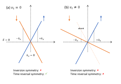
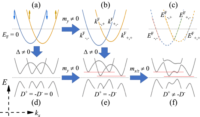
where is the Fermi velocity, and are the -Pauli matrix and identity matrix in spin space. To induce asymmetry in the spin-momentum locking, the term () tilts the dispersion [Fig. 1(b)], resulting in distinct spin-dependent counter-propagating velocities, i.e. where denotes the two opposite spins.
Systems described by Eq. (2) are suitable candidates for FEJD. The spin-momentum locking from the term breaks inversion symmetry while the asymmetry induced by breaks TRS, which is usually achieved through the Zeeman field . The simultaneous breaking of both symmetries indicates the possibility of realizing the Josephson diode without a Zeeman field (Appendix A.2).
The center-of-mass momentum of paired electrons in ASMLS is crucial to achieve FEJDs. This is modeled through the Bogoliubov-de Gennes (BdG) Hamiltonian [95] (Appendix A.3)
| (3) |
in Nambu space, where is the proximity-induced -wave SC order parameter. A non-vanishing center-of-mass momentum of paired electrons [60]
| (4) |
results from the net Fermi momentum between holes and electrons [Fig. 1(b)] with obtained by the electron and hole block dispersion in Eq. (3).
The momentum shifts the SC-gap center from to a finite energy, known as the Doppler energy shift [60] (Appendix A.4),
| (5) |
in the unit of effective SC gap . As a result, the energy of right-propagating (left-propagating) spin-up (spin-down) states increases (decreases), manifesting as spin-dependent SC gaps below [Fig. 1(c)].
II.2 Transport properties of field-effect Josephson diode
Having explained how gate-tunable center-of-mass momentum of paired electrons can be achieved, we next describe how they give rise to FEJDs with gate-controlled diode efficiency .
Our prototypical FEJD setup, based on Eq. (3), is schematically illustrated in Fig. 1(a) with super gates () applied to the left () and right () SC leads and a tunneling gate () applied to the middle non-SC region of length [40]. The SC gap and electrical potential profiles are and with macroscopic SC phases in the left/right SC leads.
Here the supercurrent is carried by ASMLSs [Fig. 1(a)]. Because of spin-momentum locking, the spin-up (spin-down) electrons are right-propagating (left-propagating), and undergo spin-flip Andreev reflections at the interfaces with the SC regions. Considering the scattering matrix at these interfaces (Appendix B), the asymmetric BdG dispersion [Fig. 1(c)] in the SC regions results in asymmetric Andreev reflection probabilities for a quasiparticle of energy , as shown in Fig. 1(d), where
| (6) |
| (7) |
In the case, identically. This asymmetry crucially arises from the nonzero Doppler energy shift and gives rise to spin-dependent Andreev bound states (ABSs) spectra, which, in the short junction limit of , (Appendix B.3) is
| (8) |
as plotted in Fig. 1(e), where is the phase difference between two SC leads. Importantly, gapless ABSs occurs when .
Through the scattering matrix formalism [96, 97], (Appendix C), we obtain the zero-temperature supercurrent,
| (9) |
where
| (10) |
with the ground-state parity , is the contribution from the ABS and
| (11) |
arise from the continuum states. Particularly, when , is solely gate-induced. For , both contributions become inseparable since disappears, and the continuous expression is .
As evident in Fig. 1(f), exhibits a sharp discontinuity at for . This has significant implications for the dissimilarity of the direction-selective critical Josephson currents, which are defined as the extrema i.e. and . In particular, for , the current reverses at and , . Intuitively, we expect the ABSs contributions to by the right-moving spin-up elections and the left-moving counterpart to be different because of the different gaps experienced, i.e. . Indeed, in the limit, the contribution is seen to enhance (suppress) the right-moving (left-moving) current, leading to .
All in all, by substituting into Eq. (1), we obtain the diode efficiency
| (12) |
which solely depends on as shown in Fig. 1(g), alongside results at nonzero temperatures . Notably, for , the diode efficiency reaches a theoretical maximum of at , which is comparable to the value obtained by applying a magnetic field [60, 67]. However, it gradually vanishes as gets larger, since in the limit, the extrema of the current becomes symmetric, as shown in Fig. 1(f).
The exclusive functional dependence of the diode efficiency on the Doppler energy shift [Eq. (5)] implies that the gate control voltage plays, in the presence of asymmetry , an indistinguishable role from that of the Zeeman field [60]. Hence, the diode efficiency can be completely gate-controlled; for instance, in the and limit, (Appendix C.2).
III Topological Feild-effect Josephson diode
The proposed FEJD might be realized in a specific type of QSHI with asymmetric helical edge states serving as the ASMLS in FEJDs. The possibility of realizing asymmetric helical edge states in QSHI is demonstrated in Sec. III.1. The helical edge states are protected by a spin-up-down parity symmetry , rather than the time-reversal symmetry [98, 99, 100]. As a result, when the spin-Chern number of the system is well-defined and non-zero, the asymmetric helical edge states [82] are expected in Floquet topological insulator [82] or magnetic-doped QSHI [84, 83].
QSHIs are ideal superconducting quantum interference devices that are proposed as a Josephson diode [61, 62]. By combining the effect of supercurrent interference and ASMLSs, the diode efficiency is greatly enhanced to , which is discussed in Sec. III.2. When considering a finite-length junction, the effect of the tunneling gate () becomes measurable, which affects the diode efficiency by tuning the interference current as illustrated in Sec. III.3.
III.1 Asymmetric helical edge states in quantum spin Hall insulator
Before diving into the field-effect behavior of the Josephson diode, we first illustrate the existence of asymmetric helical edge states in QSHI without TRS. A general ansatz of QSHI Hamiltonian is [82, 84, 83, 101, 84, 83]
| (17) | |||||
| (22) |
where , , , and . This Hamiltonian is written in the basis , where () denotes the sublattice/orbital component and () denotes the spin component of the bulk states which are distinct from the spin alignments of the edge states. The first term of Eq. (17) is the Bernevig-Hughes-Zhang Hamiltonian [101] of a QSHI with TRS which is broken by the second term induced by high-frequency circularly polarized light [82] or magnetic doping [84, 83].
It is possible to maintain the gapless edge states in a TRS-broken QSHI if the system is invariant under the up-down parity symmetry , i.e. . With this symmetry, the Hamiltonian Eq. (17) transferred into a block-diagonalized form corresponding to bispinors with only two upper or lower nonzero components that describe a quantum anomalous Hall insulator whose topology is determined by the Chern number of each block as . The spin-Chern number of the TRS-broken QSHI is thus well-defined as . The gapless edge perseveres even when TRS is broken. With a non-zero , the asymmetric helical edge states [82] is described by
| (23) |
where represents the spin orientation of the edge state, st (sb) represents the top (bottom)-edge, and is the SG applied locally on each edge.
III.2 Supercurrent interference between two edges
By specifying in Eq. (3) as Eq. (23), it is expected that the top (t) and bottom (b) edges of a QSHI each constitute an individual FEJD, with gates and Zeeman fields [82]. It is straightforward to apply Eqs. (9-12) to calculate each edge current and the diode efficiency (Appendix D.2).
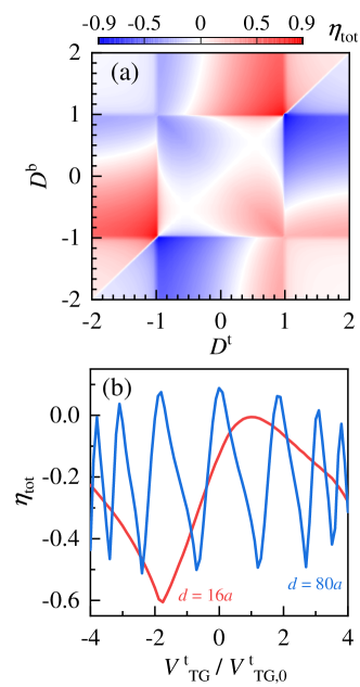
A QSHI is an ideal SC quantum interference device where the supercurrent through a device results from the interference between two ASMLS currents. As a result, the advantage of this topological implementation is to enhance through interference [61] between two topological edge currents. The combined efficiency is (Appendix D.3)
| (24) |
with and shows that when and , the diode efficiency is enhanced up to , much higher than the one in individual edge [Fig. 2(a)]. Notably, this enhancement is unattainable through a magnetic field [87, 88, 89], which cancels [89] continuum-state currents with , thereby leading to a vanishing diode effect.
III.3 Finite-length junction and numerical simulations
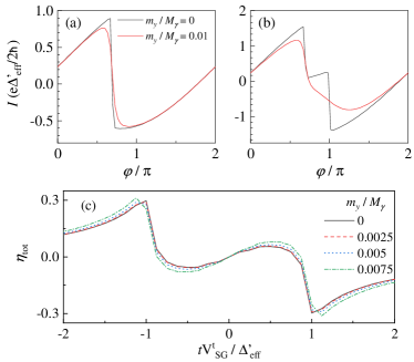
In a finite-length junction, , a phase difference between two interfering ASMLS is accumulated [82], which gives rise to with and . As a result, the phase difference between two interfering currents is controlled by the TGs and the critical current is the consequence of constructive or destructive interference leading to a TG-controlled oscillating diode efficiency [Fig. 2(b)].
The result in a finite-length junction is numerically obtained through the lattice Green’s function technique [102, 103, 82]. We set (). The width of the junction is ( is the lattice constant) which is much larger than the characteristic lengths of the edge states (), to avoid the interactions between opposite edges. In the TRS-broken term, to keep the system supporting ASMLSs with while is set for simplification. In the SC regions, the SC gap is , where is the critical temperature and is the zero-temperature SC gap. The N-SC interfaces are assumed to be transparent. SGs and TGs are applied within the areas of a width comparable to the characteristic lengths of the edge states (Appendix D.4). When manipulating the gates, the Fermi levels are restricted within the bulk gap to ensure that the supercurrent is solely contributed by the edge states. A unit gate is defined as corresponding to the phase with . Only the cases with the gate at the top edge are studied while the gate at the bottom edge is turned off ().
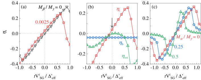
Apart from the asymmetry in helical edge states, the TRS-broken term in Eq. (17) also includes (i) the term, which is not related to the band topology but induces a spin-dependent shifting to the energy spectrum like a Zeeman field [104], and (ii) the term, which modifies the bulk band gaps and can finally, drive the system to be in a QAHI phase when . Since only the case with helical edge state is concerned here, the effect of the QAHI phase is beyond our discussion, and is set.
Our numerical results exhibit that effect (i) leads to a gate-free diode effect on each edge [Fig. 3(a)], while in the whole system, the diode effect vanishes because of the compensation between two edges [Fig. 3(b)]. The reason is the Doppler energy shift depends on via s. As a result, when , we obtain , and thus and . Effect (ii) is dual. First, the Josephson diode vanishes when the system is driven to be a QAHI, which is beyond this work due to the destruction of helical edge states. Besides, we observe that edge-state SC gap depends on both the bulk-state SC gap as expected and bulk-state band gap controlled by which is reported in Ref. [92]. Since an increasing reduces , a lower gate voltage is required to obtain the maximum value of the diode efficiency on each edge as shown in Fig. 3(c).
It is possible to induce a gap in the edge spectrum when the TRS is broken. This couples the left- and right-mover in the edge leading to a back-scattering that smoothens the skewed CPR and thus reduces the diode efficiency in each edge. However, because of the interference, the total diode efficiency can be enhanced (Appendix D.4).
IV Field-effect Josephson diodes in semiconductors
The mechanism of realizing a FEJD using ASMLSs is also attainable in semiconductors. The ASMLSs occur in semiconductors due to the interplay between the Zeeman field and the SOIs. The general Hamiltonian in the basis is [105, 106]
| (25) |
where describes the Rashba-SOI (RSOI) and Dresselhaus-SOI (DSOI) with denoting the proportion of these two components. is the in-plane Zeeman field.
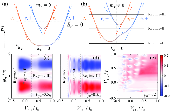
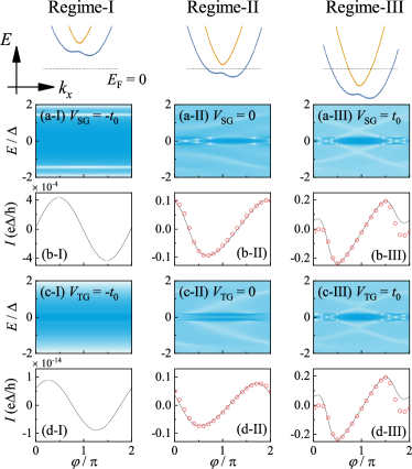
Two pairs of ASMLSs occur near [Fig. 4(a) and (b)] (Appendix E.1), resembling two edges in TRS-broken QSHIs. This is because, for example, when and (), dispersion of is shifted in direction. For the cases with other or , the shift of dispersion in momentum space is induced by different . Thus, a gate-tunable center-of-mass momentum of paired electrons is expected in a semiconductor-based FEJD.
Diode efficiencies of FEJD in the -direction exhibit three operating regimes (Appendix E.2) depending on the gate-controlled Fermi level [Fig. 4(c-e)]. In Regimes I/II/III, none/one/two ballistic SC channels across the Fermi level [Fig. 4(b)]. is absent in Regime I and oscillates with in Regime II due to the Fabry-Pérot interference between one ballistic and one tunneling channel [Fig. 4(d)] resembling the topological implementation in Fig. 2(b).
Although the mechanism of FEJD is shared with the topological FEJD due to the ASMLSs, the gate-operating performance exhibited in Fig. 4(c-e) is not as good as the topological implementation, because of the inevitable back-scattering between and due to the parallel spin-orientation component, which is forbidden in QSHI where spin orientation is tightly locked to the momentum [107, 108].
The formation of ASMLSs also accounts for the dependence of the diode efficiency on the direction of the in-plane Zeeman field. With pure RSOC (), the diode efficiency vanishes when , because of the symmetric dispersion [Fig. 4(a)]. But when the in-plane Zeeman field is parallel to , diode efficiency is maximized since the center-of-mass momentum of paired electrons is pronounced due to the maximum shift of the dispersion.
V Discussions and conclusions
As for experimental realization, semiconductor-based Josephson diodes are widely investigated in InAs [28, 29, 30] and InSb [26, 40] nanostructures. In these systems, ASMLSs are expected because of the interaction between the SOI and the in-plane magnetic field and FEJD is expected as we illustrated above. In particular, in a proximity-magnetized Pt layer by ferrimagnetic insulating Y3Fe5O12, where the ferromagnetic proximity achieves the Zeeman effect [39], a purely free-field FEJD is expected by some modifications in the current experiment setup.
Candidates of the topological FEJD are magnetic-doped QSHIs such as HgTe [110, 109], MnBi2Te4 [85, 86], and WTe2 [111, 112]. The asymmetric helical edge state may be induced by a small fixed magnetic field polarizing the magnetic atoms along a specific crystallographic -direction. The typical SC proximate gaps are in the order from meV in HgTe [80, 22] and MnBi2Te4 [85, 86] to meV in WTe2 [111, 112]. To achieve the optimized diode efficiency with , electrical potential around meV [113, 114] is required for , which guarantees the edge-state supercurrent by pining Fermi level within band gap ( meV). Corresponding critical currents ( nA) are experimentally detectable [28, 29]. Although the existence of asymmetric helical edge states is under exploration, we believe a topological FEJD could be realized shortly thanks to the development of material science.
From the two implementations of QSHI and semiconductor, we expect that the mechanism of FEJD induced by ASMLSs is universal. Although only the one-dimensional ASMLSs are studied here, similar mechanisms are also valid in systems supporting 2D/3D tilted Direc/Weyl cones such as the topological surface states in a 3D topological insulator [115, 116] and bulk states of type-I and type-II Dirac/Weyl semimetals [25]. The occurrence of ASMLSs in semiconducting systems is not restricted to the one with DSOC and RSOC that are linearly dependent on the wave vector. It is also possible to realize FEJD in more advanced systems such as semiconductors with cubic spin-orbit coupling [72].
The mechanism and the proposed FEJD are valid even if the effect of charge redistribution [117, 118, 119] is taken into account. The charge redistribution occurs at the interface between the SC leads and the central non-SC section when the Fermi levels in these regions are mismatched because of different and . With the charge redistributed, the resulting bend-bending and even band inversion effects are possible to obstacle the supercurrent non-reciprocity. The realistic gate-controlled behaviors of EFJD involving these effects are beyond this work and deserve further studies based on the solutions of the self-consistent Schrödinger–Poisson equations [119]. However, the main results of the current work are valid. The reasons are as follows. (i) FEJD can be achieved by solely controlling and keeping . As a result, no charge redistribution occurs due to the identical Fermi level between the SC and non-SC regions. In particular, in the short-junction limit, the effect of TGs in modulating the anomalous Josephson phase is negligible. (ii) In the topological FEJDs, the supercurrent carried by the asymmetric helical edge states is robust against non-magnetic potential at the interface. The effect of the charge redistribution is thus negligible, although it might be pronounced when the bulk states are involved [119]. (iii) In the semiconductor-based FEJD, the effect of the charge redistribution may become measurable and reduce the diode efficiency, but the gate-controlled behaviors of EFJD still exist [40].
In conclusion, we proposed a new mechanism to achieve FEJD, which originates from the gate-tunable center-of-mass momentum of paired electrons in ASMLS. The mechanism is schematically illustrated in Fig. 1. Based on this mechanism, we proposed a topological FEJD in a specific type of TRS-broken with asymmetric helical edge states. The diode efficiency is enhanced to due to the supercurrent interference effect between two edges. To the best of our knowledge, this is the highest theoretically predicted value in two-terminal Josephson junctions. We further demonstrate that The mechanism of realizing FEJDs via ASMLSs is also attainable in semiconductors subjected to the interplay between the Zeeman field and the SOI. Our mechanism results provide an alternative explanation to the recent experiment [40] and we expected that FEJD could be realized by some modifications in the current experiment setup. Based on these aspects, we believe our mechanism and FEJD can be achieved in future experiments and have potential applications in topological superconducting computation and cryogenic electronics.
Acknowledgements.
P.-H. F. thanks Weiping Xu, Shi-Han Zheng, Shuai Li, Jiayu Li, and Jin-Xin Hu for inspiring discussions. P.-H. F. & Y. S. A. are supported by the Singapore Ministry of Education (MOE) Academic Research Fund (AcRF) Tier 2 Grant (MOE-T2EP50221-0019). C.H.L. acknowledges support from Singapore’s NRF Quantum engineering grant NRF2021-QEP2-02-P09 and Singapore’s MOE Tier-II grant award No: MOE-T2EP50222-0003. J.-F. L. is supported by the National Natural Science Foundation of China (Grants No. 12174077), the Bureau of Education of Guangzhou Municipality (Grant No. 202255464), and the Natural Science Foundation of Guangdong Province (Grant No. 2021A1515012363).Appendix A Features of the asymmetric spin-momentum-locked Hamiltonian
In this appendix, we demonstrate the properties of the ASMLSs Hamiltonian including (i) the asymmetric spin-momentum-locking natures revealed in the group velocity of the electrons, (ii) the general requirements for the Josephson diode effect satisfied by the Hamiltonian, (iii) the gate-tunable a non-zero center-of-mass velocity and (iv) Doppler energy shift.
A.1 Hamiltonian, dispersion and asymmetric group velocity
As exhibited in Fig. 5, the dispersion of Eq. (2),
| (26) |
is tilted by , resulting in an asymmetric group velocity of the electrons
| (27) |
where the term indicates the spin-momentum-locking feature, namely, electrons propagating in spin-selective directions, and the term indicates the asymmetry – electrons with different spins counter-propagating with distinct velocities.
A.2 General requirements for Josephson diode effect
The breaking of time-reversal and inversion symmetries is the general requirement for the observation of the Josephson diode effect. The dispersion Eq. (26) with is shown in Fig. 5. When [Fig. 5(a)], the inversion symmetry is broken because states transform from to without a spin-flipping is prohibited, but the time-reversal symmetry is is preserved because it is allowed to transform from to with a spin-flipping to . When [Fig. 5(b)], both and are broken because when flipping the spin from to the state is absent because of .
Therefore, the requirement for the observation of the Josephson diode effect is met in our proposal because (i) the spin-momentum-locking nature requires a breaking of inversion symmetry, and (ii) the asymmetry breaks the time-reversal symmetry. Thus, the Josephson diode effect is expected in an ASMLS.
A.3 The non-zero center-of-mass momentum
When considering the superconducting proximity effect, the one-dimensional BdG Hamiltonian [Eq. (3)] can be written in Nambu space as
| (28) |
where
| (29) | |||||
is the Hamiltonian of the paired spin- holes with . From Eq. (26) and (29), the Fermi momentum of the electrons and holes are determined by , which are
| (30) |
The non-zero center-of-mass momentum is defined by the net Fermi momentum between the paired electrons and holes as shown in Eq. (4).
A.4 The Doppler energy shift
The dispersion of Eq. (28) is
| (31) | |||||
which is shown in Fig. 1(c) with the band edges of the upper()/lower() spin- are
| (32) |
where
| (33) |
determines the extreme value of the dispersion curve satisfying . Two modifications are induced by the asymmetry:
(i) The superconducting band gap. Defined by the difference between the upper and lower band, the superconducting band gap is
| (34) |
which is modified from to . T he effective band gap is defined for simplification.
(ii) The Doppler energy shift. The band gap center is shifted from to
which is known as the so-called Doppler energy shift induced by . Rewritten in the unit of , the Doppler energy shift [Eq. (5)] is obtained. Thus the SC gap of the occupied states () are spin-dependent, which is
| (36) |
as shown in Fig. 1(c).
Appendix B Scattering matrix and Andreev bound states
In this section, the calculation details of Andreev reflection (AR) coefficients and energy level of Andreev bound states (ABSs) are given in the framework of the scattering matrix [96, 97, 60], corresponding to Fig. 1(d) and (e) in the main text.
B.1 The wavefunctions
In a basis , the Hamiltonian describes a Josephson junction with a length supporting nonreciprocal current is
| (37) |
with
| (38) |
where the gate-voltage and SC order parameter are spatially dependent, and . Here, () is super (tunneling) gates applied in the SC lead (normal) region and () is the macroscopic phases of the left (right) SC lead. We define as the phase difference between two SC leads.
The block diagonalized BdG Hamiltonian Eq. (38) allows us to solve the scattering problem in each block separately. The electron wave function in the N region is
| (39) |
while its hole counterpart is
| (40) |
with
| (41) |
where , and () for the electron (hole) block. In the SC region, the wave function is
| (42) |
where
| (43) |
and
| (44) |
where , () for electron-like (hole-like) quasiparticles.
B.2 The scattering matrix
The propagating matrix in N region is
| (45) |
which is defined by connecting the incident wave to the the reflected/transmitted wave in the N region, . Note that, because of the spin-momentum locking (helicity), backscattering is prohibited, so we have and in Eq. (45).
Similarly, the scattering matrix connecting the wavefunctions in the AR process at the N-SC interfaces is
| (46) |
which satisfies . Note that at , we have
| (47) | |||||
| (48) |
while at , we have
| (49) | |||||
| (50) |
where and
| (51) |
with for and for . Thus Eq. (46) can be simplified as
with
| (52) |
B.3 Andreev bound states
Appendix C The current phase relations and diode efficiency
In this section, the general form of current phase relations (CPRs) using the free energy are given, corresponding to the CPR and the diode efficiency in finite and zero temperatures exhibited in Fig. 1(f) and (g). In particular, the analytical formulas of both the CPR and the diode efficiency are obtained at zero temperature by distinguishing the contributions from ABSs and continuum states.
C.1 General form
The Josephson current flowing in the sample can be determined by the free energy [60, 88, 96, 97] which is
| (55) |
where, without parity constraints [91, 87, 88], the free energy is
| (56) | |||||
By neglecting the phase-independent terms in the second line, we obtain
| (57) | |||||
where the density of states is
| (58) |
with the notion denoting the phase-independent term. Here ( is the Boltzmann constant) and the sum over energy contains both the contributions of ABSs and continuum states.
C.2 Contributions from ABSs and continuum states
When , the zero-temperature current can be decoupled as
| (62) |
where
| (63) |
and
| (64) |
are the contributions from ABS and continuum states to the current respectively. By substituting Eq. (8) into Eq. (63), we have Eq. (10) After some calculations, we obtain the current from continuum states Eq. (11), which is phase-independent and directly induced by the Doppler energy shift.
C.3 The Diode Efficiency
In the CPR [Eq. (9)], when , two critical currents are
| (66) | |||||
| (67) |
where
| (68) | |||||
| (69) |
Thus, by definition, the diode efficiency is
| (70) |
where is used.
When , two critical currents are
| (71) | |||||
| (72) |
where
| (73) | |||||
| (74) |
Then the JDE efficiency
| (75) |
Since the cosinoidal CPR in Eq. (65), the diode effect vanishes at , i.e.
| (76) |
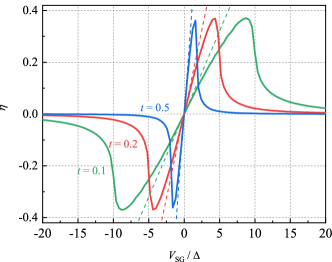
The dependence of diode efficiency with respect to the Doppler energy shift is exhibited in Fig. 1(g). Besides, the strength of asymmetry in a system can be estimated through the function diode efficiency with respect to the super gate as shown in Fig. 6, where the s linearly increase for small gate voltage with a slope relating to the strength of asymmetry.
Appendix D Topological Josephson diode
In this appendix and the following, we discuss two types of systems supporting the FEJD. One is the topological Josephson diode first proposed in this work and the others are based on semiconductors extensively operated in current experiments.
Let’s begin with the first case, including (i) a single-edge Josephson diode, (ii) a double-edge-interference Josephson diode, and (iii) the field-effect Josephson diode in a finite-length junction. The results are exhibited in Fig. 2(a) and (b).
D.1 The model
In a topological Josephson diode, the nonreciprocal current is carried by the anisotropic helical edge states, whose Hamiltonian of the spin- mode at the s edge is [82]
| (77) |
where the basis is , and
| (78) |
where is the Hamiltonian of AHES and are edge-dependent.
It is worth noting that can be induced by an in-plane Zeeman field aligned with the edge-state spin quantization axis [89] or by an (orbital) out-off plane magnetic flux inducing gauge invariant shift of momentum [87]. However, the effect of the magnetic field is global and always opposite in two edges, , canceling the diode effect in the whole junction, even though the diode efficiency is measurable in an individual edge [89]. Thus, we neglect the effect of the magnetic field by setting and the Doppler energy shift is solely controlled by the on each edge.
D.2 A single-edge Junction
The CPR, as well as the diode efficiency in a single edge, can be easily obtained by replacing the Doppler energy shift in the above sections as , which are edge-dependent. The results are listed as follows:
The CPR of a single edge is
| (79) |
and the corresponding diode efficiency is
| (80) |
D.3 Interference effect between two edge currents
A QSHI-based Josephson junction is a natural platform for a superconducting quantum interference device, where the total CPR at zero temperature is
| (81) |
whose concrete form depends on the Doppler energy shift in each edge allowing local manipulation on two currents.
We first focus on the situation with and . When , Eq. (81) is
| (82) |
where the critical currents occur near the topologically protected zero-energy crossings in ABS spectra, which are
| (83) |
and
| (84) |
The resulting diode efficiency is shown as the first line of Eq. 24. Similarly, in the case of , Eq. (81) is
| (85) |
where the critical currents are
| (86) | |||||
| (87) |
and the resulting diode efficiency is the second line of Eq. 24.
Additionally, when , since the top-edge current is negligible [Eq. (65)], the total current is dominated by the bottom-edge one and thus the diode efficiency tends to be . Therefore when and , the diode efficiency of the total Josephson current is shown as Eq. (24), which takes an analogous form for arbitrary and .
The Josephson diode efficiencies via and the CPRs are exhibited in Fig. 7. The behaviors of and are fit with Eq. (80), where the latter keeps zero due to . As increases, the low diode efficiency of when suddenly inverts and becomes relatively measurable when , while the efficiency in each edge remains low.
These phenomena are attributed to the interference between two currents and can be understood via the CPRs as shown in Fig. 7. When and , the CPRs of the two edge current are shown in Fig. 7(b). Both the positive and opposite critical currents result from the constructive interference between two edge currents, which is approximate to be in which . Thus, the resulting diode efficiency is suppressed since .
When , the CPRs are shown in Fig. 7(c). Because of the nearly cosinoidal behavior of the top-edge current [Eq. (79)], the positive (negative) critical current of occurs as , causing a destructive (constructive) interference between two currents, i.e. []. Thus, the resulting diode efficiency is , which is measurable even through the diode effects of the edge current nearly vanish.
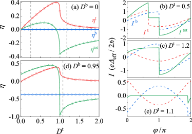
Now, by combining the effect of the interferometer and Doppler energy shift in the bottom edge, the diode efficiency is highly optimized in the region of , reaching up to when as shown in Fig. 7(c).
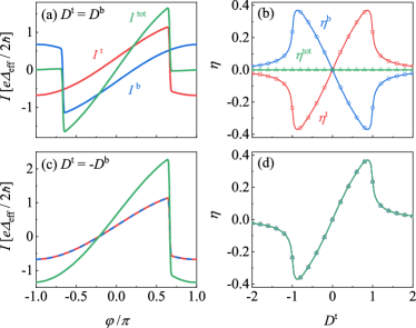
Generally, a fully polarized diode with is impossible. This is restricted by the relation , which indicates that when the critical current in one direction is zero, its opposite-direction counterpart must vanish. As shown in Fig. 7(d), even though the positive critical current is nearly zero in a wide range of , the negative critical current only survives in a tiny range of .
Note that when , the corresponding current vanished, and the diode reduces to . Thus, in this situation, the current in a double junction is always larger than the one in a single junction.
It is worth noting that two special cases where the Doppler energy shift in each edge is identical and opposite to each other, as shown in Fig. (8). In the former, no diode effect is expected, even though the supercurrent is asymmetric on each edge. This is the reason why no Josephson diode effect is achieved by applying a magnetic field [87, 89]. On the other hand, in the latter case, the total diode effect behavior with the same tendency as the ones in each edge. This suggests that a topological FEJD can be realized in a time-reversal broken QSHI tunning a transverse electrical field [82]
D.4 Numerical simulations for field-effect topological Josephson diode
So far, only the super-gate-controlled topological Josephson diode is discussed due to the negligible effect of the tunneling gate with the assumption of . For a junction of finite length, a field-effect topological Josephson diode is expected in the numerical simulations, where the tunneling gate can switch the diode on and off and even reverse the diode polarity.
D.4.1 Tight-binding model and lattice Green’s function
By substituting and with and and using Fourier transformation, Eq. (17) can be rewritten in a square lattice. The Hamiltonian of the Josephson junction is
| (88) |
where
| (89) |
and
| (90) |
are the Hamiltonian in the N region and left/right SC leads, respectively. And
| (91) |
couples the left/right SC to the central region. Here, with and () is the annihilation (creation) operator of / orbit electron at site with spin / and the notion represents spin up and down.
The components are
| (92) | |||||
| (93) | |||||
| (94) | |||||
| (95) |
where () is the unit (the third Pauli) matrix in Nambu space, and
| (96) | |||||
| (97) | |||||
| (98) | |||||
| (99) | |||||
| (100) |
In the numerical calculations we choose for simplification and the Fermi level is controlled by , which is spatially dependent,
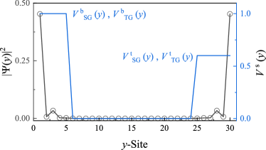
The distribution of along -direction is shown in Fig. 9 compared with the wave function of the edge states.
With the discussion above, using lattice Green’s function method, the Josephson current through column in the N region is [103, 102]
| (102) |
where is the charge matrix. In equilibrium, the lesser-than-Green’s function is calculated by where is the Fermi-Dirac distribution function. The retarded Green’s function is
| (103) |
and , where is the Hamiltonian of an individual column and the retarded self-energy representing the coupling with left/right SC lead can be calculated numerically by the recursive method.
To understand the behavior of Josephson current, one can calculate ABS spectra through Green’s function technique numerically. The energies of ABS levels can be located by searching the peaks of particle density within the SC gap at column
| (104) |
at a given phase difference .
D.4.2 Remarks on the numerical results
As is observed in Eq. (17), the effects of TRS-breaking term on the QSHI include:
(i) the asymmetry to the helical edge states through the terms proportional to ,
(ii) the term, which is not related to the band topology but induces a spin-dependent shifting to the energy spectrum like a Zeeman field, and
(iii) the term, which modifies the bulk band gaps and can finally, drive the system to be in a QAHI phase when .
Based on the observation of the numerical results, the three effects on the Josephson diode are concluded below.
Effect (i) leads to the gate-controlled Josephson diode which is the main claim of this work.
Effect (ii) leads to a gate-free diode effect on each edge [Fig. 3(a)], while in the whole system, the diode effect vanishes because of the compensation between two edges [Fig. 3(b)]. The reason is the Doppler energy shift depends on via s. As a result, when , we obtain , and thus and . One of the motivations of this work is the complementary effect between the electrical potential and the Zeeman field .
Effect (iii) is dual. First, the Josephson diode vanishes when the system is driven to be a QAHI, which is beyond this work due to the destruction of helical edge states. Besides, we observe that edge-state superconducting gap depends on both the bulk-state superconducting gap as expected and bulk-state band gap controlled by which is reported in Ref. [92]. Since an increasing reduces , a lower gate voltage is required to obtain the maximum value of the diode efficiency on each edge as shown in Fig. 3.
On the other hand, it is possible to induce a gap in the edge spectrum by when the TRS is broken. This couples the left- and right-mover in the edge leading to a back-scattering that smoothens the skewed CPR and thus reduces the diode efficiency in one edge as shown in Fig. 10(a). However, because of the interference, the total diode efficiency is enhanced [Fig. 10(b) and (c)].
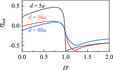
When the junction length increases, as shown in Fig. 11, even though the short-junction condition preserves (), the behavior of via deviates from the Eq. (24), but a relatively high-efficiency diode keeps when the gate is finely tuned. Such a deviation may be attributed to the additional phase accumulated by the non-zero center-of-mass velocity, which reduces the interference effect and thus suppresses the diode efficiency.
However, the phase difference between two interfering currents can be controlled by the TG, resulting in a field-effect Josephson diode transistor. This manifests in oscillating diode efficiency with respect to the gate at the top edge as shown in Fig. 2(b), with an oscillating frequency increasing as the junction length grows. In the diode transistor, the diode effect can be switched on with an efficiency up to when , and the polarity can be rapidly reversed when .
Appendix E Semiconductor-based Josephson diode
In this appendix, we demonstrate that the framework of the ASMLSs can explain the gate-tunability of the semiconductors Josephson diode investigated in recent experiments [40].
We first exhibit that ASMLSs occur, when the Zeeman field is aligned with the spin-orbit field that couples to the momentum parallel to the current as illustrated in Fig. 12. Then, the gate-tunability of the Josephson diode is numerically studied in the systems including a theoretical model of 1D limit and the experimentally concerned 2D nanoflakes.
The mechanism of the gate-tunability is explained by investigating the ABS and CPR exhibited in Fig. 13. The diode efficiency is controlled by the gate through the electron density. In low (here is negative) gate voltage (Regime-I in Fig. 13), the system is an insulator and low electron density around the Fermi level fails to support the formation of Cooper pairs. Thus there is no Josephson current as well as the diode effect. For a medium gate voltage (Regime-II in Fig. 13), the system is a half metal, where one of the two channels is activated with high transmission probability, while the other channel keeps in the tunneling regime. The interference between two currents causes a tunneling-gate-control oscillating diode efficiency [Fig. (4)] resembling double-junction interference in topological FEJD. Finally, two ballistic Josephson channels are activated by the high gate voltage (Regime-III in Fig. 13), and the diode oscillation is suppressed due to the constructive interference between the currents.
E.1 Asymmetric spin-momentum-locking states around Fermi surface
We consider a 2D electron gas (EG) with a strong spin-orbit interaction (SOI) and subjected to a Zeeman splitting. The Hamiltonian is shown as Eq. (25). Similarly, when taking the SC proximity effect into account, the BdG Hamiltonian of Eq. (25) is
| (105) |
For the 1D limit of with , pure RSOI (), and , the Hamiltonian Eq. (25) is reduced as
| (106) |
whose dispersion is
| (107) |
As shown in Fig. 12, with the magnetic field aligned with the spin-orbit field direction, the band-touching nodes shift accompanied by a band tilting resulting in an ASML.
To illustrate within the framework of ASML, we rotate the spin polarization axis along the spin-orbit field and the Eq. (106) can be rewritten as
| (108) | |||||
where
| (109) |
Assuming that the Fermi energy is zero, the Fermi wavenumbers are
| (110) |
with and as shown in Fig. 12(b). The Hamiltonian around Fermi surface can be written in the basis as
| (111) |
with
| (112) |
where () describe the states with a larger (smaller) magnitude of Fermi wavenumber and
| (113) |
is obtained by expanding Eq. (107) around . A comparative plot in Fig. 12(c) verifies this effectiveness.
After a further rearrangement, Eq. (112) has the same form as Eq. (23) supporting ASMLSs, which is
| (114) |
where and
| (115) | |||||
| (116) | |||||
| (117) | |||||
| (118) |
However, when considering the SC proximity effect in Eq. (105), the effect of the Doppler energy shift in two subbands always cancels each other, because
| (119) |
as shown in Fig. 12(e) and no diode effect is expected.
This degeneracy is destroyed by the magnetic field component perpendicular to the spin-orbit field shown in Fig. 12(f). Thus, both the Zeeman-field components parallel to and perpendicular to the spin-orbit field are necessary for the Josephson diode, which is verified in Fig. 4 through the numerical calculations below.
E.2 Results and discussions
E.2.1 The tight-binding model
The tight-binding version of Eq. (105) is
| (120) |
where is the site index, in the unit vector and is the hopping matrix along three directions. The components in Eq. (120) are
| (121) | |||||
| (122) | |||||
| (123) |
combined with the lattice Green’s function, the Josephson current and the ABS can be obtained. The junction width is , the Landé -factors are isotropic and both RSOI and DSOI are considered.
| Fig.13 | ||||||
|---|---|---|---|---|---|---|
| (b-II) | ||||||
| (b-III) | ||||||
| (d-II) | ||||||
| (d-III) |
E.2.2 Results and explanations
Phenomenologically, there are two subband contributions to the total current, which can be expressed as and
where , , , and are the critical current, ground-state phase difference and the averaged transmission probability and the contribution from Doppler energy shift in the subband, respectively. The parameters satisfying the fit with numerical results are shown in Table 1. In Regime I of Fig. 13 with , , the system is an insulator and the low electron density fails to support Cooper-pair formation in the SC Region and propagating electron-hole pairs in the N Region, respectively. Thus, no Josephson current and diode effect is allowed due to the low transmission probability and contribution from non-zero center-of-mass velocity (, ) as shown in Fig. 13(b-I) and (d-I). No numerical fit is considered because this case is not important to our results.
When , are in Regime II, the system is half metal, where only one of the subbands is occupied resulting in one Josephson ballistic channel () with measurable contribution from non-zero center-of-mass velocity () while the other channel from the unoccupied subbands keeps in tunneling regime () and . In both channels, there is a ground-state phase difference accumulated in the finite-length N region. This is justified in Fig. 13(b-II) and (d-II), where the numerical results can be fit by choosing suitable parameters in Eq. (E.2.2).
Finally, when , are in Regime III, both ballistic channels are activated. Since the interference between two channels is always constructive, and the ground-state phase differences are opposite, the diode efficiency oscillation is suppressed as shown in Fig. 13(b-III) and (d-III).
E.2.3 Potential relation to the experiments
Numerically, the current can be obtained through
| (125) |
where can be calculated using the Green’s function technique as in the 1D case with additional parameters relevant to ( is an integer). The diode efficiency is obtained in the CPR.
The dependence of diode efficiency on both the in-plane direction of the magnetic field and the gate voltage is exhibited in Fig. 4, where the three regimes regarding zero-, one- and two-channel contributions controlled by the gates are expected, consistent with the discussions in 1D case. Besides, the diode efficiency oscillates as the TG varies.
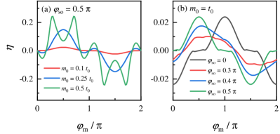
Another feature of diode efficiency with respect to the magnetic field is with as shown in Fig. 14(a). For a weak field intensity, the dependence of diode efficiency on is not a simple sinusoidal function [] as observed in Ref. [40], but contains more higher-order terms with , and only the first several orders dominate the contribution as the field intensity slightly increases. Furthermore, with a stronger field, the function of is intricate with a tendency as and .
Besides, in the weak-field situation, it is expected that the diode efficiency maximum occurs when as a signature of the alignment between the direction of the external magnetic field and the internal spin-orbit field. However, in our results, such a statement is only valid for a system with pure RSOI () or pure DSOI () as exhibited in Fig. 14(b). In the system with max SOI, the maximum of do not occur at and their behavior can not capture by a simple expression as well.
References
- [1] M. Fruchart, R. Hanai, P. B. Littlewood, and V. Vitelli, Non-Reciprocal Phase Transitions, Nature 592, 363 (2021).
- [2] H. Zhang, T. Chen, L. Li, C. H. Lee, and X. Zhang, Electrical Circuit Realization of Topological Switching for the Non-Hermitian Skin Effect, Phys. Rev. B 107, 085426 (2023).
- [3] X. Zhao, Y. Xing, J. Cao, S. Liu, W.-X. Cui, and H.-F. Wang, Engineering Quantum Diode in One-Dimensional Time-Varying Superconducting Circuits, Npj Quantum Inf. 9, 59 (2023).
- [4] A. Stegmaier et al., Realizing Efficient Topological Temporal Pumping in Electrical Circuits, arXiv: 2306.15434 (2023).
- [5] S. M. Sze, & M.-K. Lee, Semiconductor Devices: Physics and Technology 3rd edn (Wiley, 2012).
- [6] M. Nadeem, M. S. Fuhrer, and X. Wang, The Superconducting Diode Effect, Nat. Rev. Phys. 5, 558 (2023).
- [7] R. Wakatsuki, Y. Saito, S. Hoshino, Y. M. Itahashi, T. Ideue, M. Ezawa, Y. Iwasa, and N. Nagaosa, Nonreciprocal Charge Transport in Noncentrosymmetric Superconductors, Sci. Adv. 3, e1602390 (2017).
- [8] E. Zhang, X. Xu, Y.-C. Zou, L. Ai, X. Dong, C. Huang, P. Leng, S. Liu, Y. Zhang, Z. Jia, X. Peng, M. Zhao, Y. Yang, Z. Li, H. Guo, S. J. Haigh, N. Nagaosa, J. Shen, and F. Xiu, Nonreciprocal Superconducting NbSe2 Antenna, Nat. Commun. 11, 5634 (2020).
- [9] F. Ando, Y. Miyasaka, T. Li, J. Ishizuka, T. Arakawa, Y. Shiota, T. Moriyama, Y. Yanase, and T. Ono, Observation of Superconducting Diode Effect, Nature 584, 373 (2020).
- [10] T. Schumann, L. Galletti, H. Jeong, K. Ahadi, W. M. Strickland, S. Salmani-Rezaie, and S. Stemmer, Possible Signatures of Mixed-Parity Superconductivity in Doped Polar SrTiO3 Films, Phys. Rev. B 101, 100503(R) (2020).
- [11] L. Bauriedl, C. Bäuml, L. Fuchs, C. Baumgartner, N. Paulik, J. M. Bauer, K.-Q. Lin, J. M. Lupton, T. Taniguchi, K. Watanabe, C. Strunk, and N. Paradiso, Supercurrent Diode Effect and Magnetochiral Anisotropy in Few-Layer NbSe2, Nat. Commun. 13, 4266 (2022).
- [12] Y. M. Itahashi, T. Ideue, Y. Saito, S. Shimizu, T. Ouchi, T. Nojima, and Y. Iwasa, Nonreciprocal Transport in Gate-Induced Polar Superconductor SrTiO3, Sci. Adv. 6, eaay9120 (2020).
- [13] J. Yun, S. Son, J. Shin, G. Park, K. Zhang, Y. J. Shin, J.-G. Park, and D. Kim, Magnetic Proximity-Induced Superconducting Diode Effect and Infinite Magnetoresistance in a van Der Waals Heterostructure, Phys. Rev. Res. 5, L022064 (2023).
- [14] Y.-Y. Lyu, J. Jiang, Y.-L. Wang, Z.-L. Xiao, S. Dong, Q.-H. Chen, M. V. Milošević, H. Wang, R. Divan, J. E. Pearson, P. Wu, F. M. Peeters, and W.-K. Kwok, Superconducting Diode Effect via Conformal-Mapped Nanoholes, Nat. Commun. 12, 2703 (2021).
- [15] K. Yasuda, H. Yasuda, T. Liang, R. Yoshimi, A. Tsukazaki, K. S. Takahashi, N. Nagaosa, M. Kawasaki, and Y. Tokura, Nonreciprocal Charge Transport at Topological Insulator/Superconductor Interface, Nat. Commun. 10, 2734 (2019).
- [16] Y. Wu, Q. Wang, X. Zhou, J. Wang, P. Dong, J. He, Y. Ding, B. Teng, Y. Zhang, Y. Li, C. Zhao, H. Zhang, J. Liu, Y. Qi, K. Watanabe, T. Taniguchi, and J. Li, Nonreciprocal Charge Transport in Topological Kagome Superconductor CsV3Sb5, arXiv: 2210.10437 (2022).
- [17] M. Masuko, M. Kawamura, R. Yoshimi, M. Hirayama, Y. Ikeda, R. Watanabe, J. J. He, D. Maryenko, A. Tsukazaki, K. S. Takahashi, M. Kawasaki, N. Nagaosa, and Y. Tokura, Nonreciprocal Charge Transport in Topological Superconductor Candidate Bi2Te3/PdTe2 Heterostructure, Npj Quantum Mater. 7, 104 (2022).
- [18] Y. Hou, F. Nichele, H. Chi, A. Lodesani, Y. Wu, M. F. Ritter, D. Z. Haxell, M. Davydova, S. Ilić, O. Glezakou-Elbert, A. Varambally, F. S. Bergeret, A. Kamra, L. Fu, P. A. Lee, and J. S. Moodera, Ubiquitous Superconducting Diode Effect in Superconductor Thin Films, Phys. Rev. Lett. 131, 027001 (2023).
- [19] J.-X. Lin, P. Siriviboon, H. D. Scammell, S. Liu, D. Rhodes, K. Watanabe, T. Taniguchi, J. Hone, M. S. Scheurer, and J. I. A. Li, Zero-Field Superconducting Diode Effect in Small-Twist-Angle Trilayer Graphene, Nat. Phys. 18, 1221 (2022).
- [20] J. Jiang, M. V. Milošević, Y.-L. Wang, Z.-L. Xiao, F. M. Peeters, and Q.-H. Chen, Field-Free Superconducting Diode in a Magnetically Nanostructured Superconductor, Phys. Rev. Appl. 18, 034064 (2022).
- [21] H. Narita, J. Ishizuka, R. Kawarazaki, D. Kan, Y. Shiota, T. Moriyama, Y. Shimakawa, A. V. Ognev, A. S. Samardak, Y. Yanase, and T. Ono, Field-Free Superconducting Diode Effect in Noncentrosymmetric Superconductor/Ferromagnet Multilayers, Nat. Nanotechnol. 17, 823 (2022).
- [22] E. Bocquillon, R. S. Deacon, J. Wiedenmann, P. Leubner, T. M. Klapwijk, C. Brüne, K. Ishibashi, H. Buhmann, and L. W. Molenkamp, Gapless Andreev Bound States in the Quantum Spin Hall Insulator HgTe, Nat. Nanotechnol. 12, 137 (2017).
- [23] J. Diez-Merida, A. Diez-Carlon, S. Y. Yang, Y.-M. Xie, X.-J. Gao, K. Watanabe, T. Taniguchi, X. Lu, K. T. Law, and D. K. Efetov, Magnetic Josephson Junctions and Superconducting Diodes in Magic Angle Twisted Bilayer Graphene, arXiv: 2110.01067 (2021).
- [24] E. Portolés, S. Iwakiri, G. Zheng, P. Rickhaus, T. Taniguchi, K. Watanabe, T. Ihn, K. Ensslin, and F. K. de Vries, A Tunable Monolithic SQUID in Twisted Bilayer Graphene, Nat. Nanotechnol. 17, 1159 (2022).
- [25] B. Pal, A. Chakraborty, P. K. Sivakumar, M. Davydova, A. K. Gopi, A. K. Pandeya, J. A. Krieger, Y. Zhang, M. Date, S. Ju, N. Yuan, N. B. M. Schröter, L. Fu, and S. S. P. Parkin, Josephson Diode Effect from Cooper Pair Momentum in a Topological Semimetal, Nat. Phys. 18, 1228 (2022).
- [26] B. Turini, S. Salimian, M. Carrega, A. Iorio, E. Strambini, F. Giazotto, V. Zannier, L. Sorba, and S. Heun, Josephson Diode Effect in High Mobility InSb Nanoflags, Nano Lett. 22, 8502 (2022).
- [27] M. Gupta, G. V. Graziano, M. Pendharkar, J. T. Dong, C. P. Dempsey, C. Palmstrøm, and V. S. Pribiag, Gate-Tunable Superconducting Diode Effect in a Three-Terminal Josephson Device, Nat. Commun. 14, 3078 (2023).
- [28] C. Baumgartner, L. Fuchs, A. Costa, S. Reinhardt, S. Gronin, G. C. Gardner, T. Lindemann, M. J. Manfra, P. E. Faria Junior, D. Kochan, J. Fabian, N. Paradiso, and C. Strunk, Supercurrent Rectification and Magnetochiral Effects in Symmetric Josephson Junctions, Nat. Nanotechnol. 17, 39 (2022).
- [29] C. Baumgartner, L. Fuchs, A. Costa, J. Picó-Cortés, S. Reinhardt, S. Gronin, G. C. Gardner, T. Lindemann, M. J. Manfra, P. E. Faria Junior, D. Kochan, J. Fabian, N. Paradiso, and C. Strunk, Effect of Rashba and Dresselhaus Spin-Orbit Coupling on Supercurrent Rectification and Magnetochiral Anisotropy of Ballistic Josephson Junctions, J. Phys. Condens. Matter 34, 154005 (2022).
- [30] A. Costa, C. Baumgartner, S. Reinhardt, J. Berger, S. Gronin, G. C. Gardner, T. Lindemann, M. J. Manfra, D. Kochan, J. Fabian, N. Paradiso, and C. Strunk, Sign Reversal of the Josephson Inductance Magnetochiral Anisotropy and --like Transitions in Supercurrent Diodes Nat. Nanotechnol. 18, 1266 (2023).
- [31] M. S. Anwar, T. Nakamura, R. Ishiguro, S. Arif, J. W. A. Robinson, S. Yonezawa, M. Sigrist, and Y. Maeno, Spontaneous Superconducting Diode Effect in Non-Magnetic Nb/Ru/Sr2RuO4 Topological Junctions, Commun. Phys. 6, 290 (2023).
- [32] S. Ghosh, V. Patil, A. Basu, Kuldeep, D. A. Jangade, R. Kulkarni, A. Thamizhavel, and M. M. Deshmukh, High-Temperature Superconducting Diode, arXiv: 2210.11256 (2022).
- [33] J. Chiles, E. G. Arnault, C.-C. Chen, T. F. Q. Larson, L. Zhao, K. Watanabe, T. Taniguchi, F. Amet, and G. Finkelstein, Nonreciprocal Supercurrents in a Field-Free Graphene Josephson Triode, Nano Lett. 23, 5257 (2023).
- [34] M. Trahms, L. Melischek, J. F. Steiner, B. Mahendru, I. Tamir, N. Bogdanoff, O. Peters, G. Reecht, C. B. Winkelmann, F. von Oppen, and K. J. Franke, Diode Effect in Josephson Junctions with a Single Magnetic Atom, Nature 615, 628 (2023).
- [35] X. Song, S. Suresh-Babu, Y. Bai, D. Golubev, I. Burkova, A. Romanov, E. Ilin, J. N. Eckstein, and A. Bezryadin, Interference, Diffraction, and Diode Effects in Superconducting Array Based on Bismuth Antimony Telluride Topological Insulator, Commun. Phys. 6, 177 (2023).
- [36] T. Golod and V. M. Krasnov, Demonstration of a Superconducting Diode-with-Memory, Operational at Zero Magnetic Field with Switchable Nonreciprocity, Nat. Commun. 13, 3658 (2022).
- [37] F. Zhang, M. T. Ahari, A. S. Rashid, G. J. de Coster, T. Taniguchi, K. Watanabe, M. J. Gilbert, N. Samarth, and M. Kayyalha, Reconfigurable Magnetic-Field-Free Superconducting Diode Effect in Multi-Terminal Josephson Junctions, arXiv: 2301.05081 (2023).
- [38] H. Wu, Y. Wang, Y. Xu, P. K. Sivakumar, C. Pasco, U. Filippozzi, S. S. P. Parkin, Y.-J. Zeng, T. McQueen, and M. N. Ali, The Field-Free Josephson Diode in a van Der Waals Heterostructure, Nature 604, 653 (2022).
- [39] K.-R. Jeon, J.-K. Kim, J. Yoon, J.-C. Jeon, H. Han, A. Cottet, T. Kontos, and S. S. P. Parkin, Zero-Field Polarity-Reversible Josephson Supercurrent Diodes Enabled by a Proximity-Magnetized Pt Barrier, Nat. Mater. 21, 1008 (2022).
- [40] G. P. Mazur, N. van Loo, D. van Driel, J.-Y. Wang, G. Badawy, S. Gazibegovic, E. P. A. M. Bakkers, and L. P. Kouwenhoven, The Gate-Tunable Josephson Diode, arXiv: 2211.14283 (2022).
- [41] S. Hoshino, R. Wakatsuki, K. Hamamoto, and N. Nagaosa, Nonreciprocal Charge Transport in Two-Dimensional Noncentrosymmetric Superconductors, Phys. Rev. B 98, 054510 (2018).
- [42] R. Wakatsuki and N. Nagaosa, Nonreciprocal Current in Noncentrosymmetric Rashba Superconductors, Phys. Rev. Lett. 121, 026601 (2018).
- [43] B. Zhai, B. Li, Y. Wen, F. Wu, and J. He, Prediction of Ferroelectric Superconductors with Reversible Superconducting Diode Effect, Phys. Rev. B 106, L140505 (2022).
- [44] J. J. He, Y. Tanaka, and N. Nagaosa, A Phenomenological Theory of Superconductor Diodes, New J. Phys. 24, 053014 (2022).
- [45] H. D. Scammell, J. I. A. Li, and M. S. Scheurer, Theory of Zero-Field Superconducting Diode Effect in Twisted Trilayer Graphene, 2D Mater. 9, 025027 (2022).
- [46] S. Ilić and F. S. Bergeret, Theory of the Supercurrent Diode Effect in Rashba Superconductors with Arbitrary Disorder, Phys. Rev. Lett. 128, 177001 (2022).
- [47] N. F. Q. Yuan and L. Fu, Supercurrent diode effect and finite-momentum superconductors, Proc. Natl. Acad. Sci. USA 119, e2119548119 (2022).
- [48] A. Daido, Y. Ikeda, and Y. Yanase, Intrinsic Superconducting Diode Effect, Phys. Rev. Lett. 128, 037001 (2022).
- [49] A. Daido and Y. Yanase, Superconducting Diode Effect and Nonreciprocal Transition Lines, Phys. Rev. B 106, 205206 (2022).
- [50] H. F. Legg, D. Loss, and J. Klinovaja, Superconducting Diode Effect Due to Magnetochiral Anisotropy in Topological Insulators and Rashba Nanowires, Phys. Rev. B 106, 104501 (2022).
- [51] C.-Z. Chen, J. J. He, M. N. Ali, G.-H. Lee, K. C. Fong, and K. T. Law, Asymmetric Josephson Effect in Inversion Symmetry Breaking Topological Materials, Phys. Rev. B 98, 075430 (2018).
- [52] A. A. Kopasov, A. G. Kutlin, and A. S. Mel’nikov, Geometry Controlled Superconducting Diode and Anomalous Josephson Effect Triggered by the Topological Phase Transition in Curved Proximitized Nanowires, Phys. Rev. B 103, 144520 (2021).
- [53] K. Misaki and N. Nagaosa, Theory of the Nonreciprocal Josephson Effect, Phys. Rev. B 103, 245302 (2021).
- [54] K. Halterman, M. Alidoust, R. Smith, and S. Starr, Supercurrent Diode Effect, Spin Torques, and Robust Zero-Energy Peak in Planar Half-Metallic Trilayers, Phys. Rev. B 105, 104508 (2022).
- [55] Y. Wei, H.-L. Liu, J. Wang, and J.-F. Liu, Supercurrent Rectification Effect in Graphene-Based Josephson Junctions, Phys. Rev. B 106, 165419 (2022).
- [56] Y.-M. Xie, D. K. Efetov, and K. T. Law, -Josephson Junction in Twisted Bilayer Graphene Induced by a Valley-Polarized State, Phys. Rev. Res. 5, 023029 (2023).
- [57] Y. Zhang, Y. Gu, P. Li, J. Hu, and K. Jiang, General Theory of Josephson Diodes, Phys. Rev. X 12, 041013 (2022).
- [58] A. Soori, Nonequilibrium Josephson Diode Effect in Periodically Driven SNS Junctions, Phys. Scr. 98, 065917 (2023).
- [59] A. Soori, Anomalous Josephson Effect and Rectification in Junctions between Floquet Topological Superconductors, Phys. E Low-Dimensional Syst. Nanostructures 146, 115545 (2023).
- [60] M. Davydova, S. Prembabu, and L. Fu, Universal Josephson Diode Effect, Sci. Adv. 8, eabo0309 (2022).
- [61] R. S. Souto, M. Leijnse, and C. Schrade, Josephson Diode Effect in Supercurrent Interferometers, Phys. Rev. Lett. 129, 267702 (2022).
- [62] Y. V. Fominov and D. S. Mikhailov, Asymmetric Higher-Harmonic SQUID as a Josephson Diode, Phys. Rev. B 106, 134514 (2022).
- [63] J.-X. Hu, Z.-T. Sun, Y.-M. Xie, and K. T. Law, Josephson Diode Effect Induced by Valley Polarization in Twisted Bilayer Graphene, Phys. Rev. Lett. 130, 266003 (2023).
- [64] R. Haenel and O. Can, Superconducting Diode from Flux Biased Josephson Junction Arrays, arXiv: 2212.02657 (2022).
- [65] J. F. Steiner, L. Melischek, M. Trahms, K. J. Franke, and F. von Oppen, Diode Effects in Current-Biased Josephson Junctions, Phys. Rev. Lett. 130, 177002 (2023).
- [66] T. H. Kokkeler, A. A. Golubov, and F. S. Bergeret, Field-Free Anomalous Junction and Superconducting Diode Effect in Spin-Split Superconductor/Topological Insulator Junctions, Phys. Rev. B 106, 214504 (2022).
- [67] B. Lu, S. Ikegaya, P. Burset, Y. Tanaka, and N. Nagaosa, Tunable Josephson Diode Effect on the Surface of Topological Insulators, Phys. Rev. Lett. 131, 096001 (2023).
- [68] Y. Tanaka, B. Lu, and N. Nagaosa, Theory of Giant Diode Effect in -Wave Superconductor Junctions on the Surface of a Topological Insulator, Phys. Rev. B 106, 214524 (2022).
- [69] H. F. Legg, K. Laubscher, D. Loss, and J. Klinovaja, Parity-Protected Superconducting Diode Effect in Topological Josephson Junctions, Phys. Rev. B 108, 214520 (2023).
- [70] T. Karabassov, I. V. Bobkova, V. M. Silkin, B. G. Lvov, A. A. Golubov, and A. S. Vasenko, Phase Diagrams of the Diode Effect in Superconducting Heterostructures, Phys. Scr. 99, 015010 (2024).
- [71] A. Maiani, K. Flensberg, M. Leijnse, C. Schrade, S. Vaitiekėnas, and R. S. Souto, Nonsinusoidal Current-Phase Relations in Semiconductor-Superconductor-Ferromagnetic Insulator Devices, Phys. Rev. B 107, 245415 (2023).
- [72] M. Alidoust, C. Shen, and I. Žutić, Cubic Spin-Orbit Coupling and Anomalous Josephson Effect in Planar Junctions, Phys. Rev. B 103, L060503 (2021).
- [73] P. Ding, C. H. Lee, X. Wu, and R. Thomale, Diagnosis of pairing symmetry by vortex and edge spectra in kagome superconductors, Phys. Rev. B 105, 174518 (2022).
- [74] P. Ding, T. Schwemmer, C. H. Lee, X. Wu, and R. Thomale, Hyperbolic Fringe Signal for Twin Impurity Quasiparticle Interference, Phys. Rev. Lett. 130, 256001 (2023)
- [75] B. Zinkl, K. Hamamoto, and M. Sigrist, Symmetry Conditions for the Superconducting Diode Effect in Chiral Superconductors, Phys. Rev. Res. 4, 033167 (2022).
- [76] J. Hu, C. Wu, and X. Dai, Proposed Design of a Josephson Diode, Phys. Rev. Lett. 99, 067004 (2007).
- [77] D. Wang, Q.-H. Wang, and C. Wu, Symmetry Constraints on Direct-Current Josephson Diodes, arXiv: 2209.12646 (2022).
- [78] N. F. Q. Yuan and L. Fu, Zeeman-Induced Gapless Superconductivity with a Partial Fermi Surface, Phys. Rev. B 97, 115139 (2018).
- [79] N. F. Q. Yuan and L. Fu, Topological Metals and Finite-Momentum Superconductors, Proc. Natl. Acad. Sci. 118 (3) e2019063118 (2021).
- [80] S. Hart, H. Ren, M. Kosowsky, G. Ben-Shach, P. Leubner, C. Brüne, H. Buhmann, L. W. Molenkamp, B. I. Halperin, and A. Yacoby, Controlled Finite Momentum Pairing and Spatially Varying Order Parameter in Proximitized HgTe Quantum Wells, Nat. Phys. 13, 87 (2017).
- [81] R. S. Muller, T. I. Kamins, & M. Chan, Device Electronics for Integrated Circuits 3rd edn (John Wiley & Sons, Inc., 2003).
- [82] P.-H. Fu, Y. Xu, X.-L. Yu, J.-F. Liu, and J. Wu, Electrically Modulated Josephson Junction of Light-Dressed Topological Insulators, Phys. Rev. B 105, 064503 (2022).
- [83] D. Zhang, M. Shi, T. Zhu, D. Xing, H. Zhang, and J. Wang, Topological Axion States in the Magnetic Insulator MnBi2Te4 with the Quantized Magnetoelectric Effect, Phys. Rev. Lett. 122, 206401 (2019).
- [84] C.-Z. Chen, J. Qi, D.-H. Xu, and X. Xie, Evolution of Berry Curvature and Reentrant Quantum Anomalous Hall Effect in an Intrinsic Magnetic Topological Insulator, Sci. China Physics, Mech. Astron. 64, 127211 (2021).
- [85] J. Chen, W. Xu, Z. Tan, Z. Pan, P. Zhu, Z.-M. Liao, and D. Yu, Superconducting Proximity in Intrinsic Magnetic Topological Insulator MnBi2Te4-NbN Hybrid Device Modulated by Coulomb Blockade Effect, Nano Lett. 22, 6484 (2022).
- [86] W.-Z. Xu, C.-G. Chu, Z.-C. Pan, J.-J. Chen, A.-Q. Wang, Z.-B. Tan, P.-F. Zhu, X.-G. Ye, D.-P. Yu, and Z.-M. Liao, Proximity-Induced Superconducting Gap in the Intrinsic Magnetic Topological Insulator MnBi2 Te4, Phys. Rev. B 105, 184515 (2022).
- [87] G. Tkachov, P. Burset, B. Trauzettel, and E. M. Hankiewicz, Quantum interference of edge supercurrents in a two-dimensional topological insulator, Phys. Rev. B 92, 045408 (2015).
- [88] B. Scharf, A. Braggio, E. Strambini, F. Giazotto, and E. M. Hankiewicz, Thermodynamics in Topological Josephson Junctions, Phys. Rev. Res. 3, 033062 (2021).
- [89] F. Dolcini, M. Houzet, and J. S. Meyer, Topological Josephson junctions, Phys. Rev. B 92,035428 (2015).
- [90] M. Alidoust and H. Hamzehpour, Spontaneous Supercurrent and Phase Shift Parallel to Magnetized Topological Insulator Interfaces, Phys. Rev. B 96, 165422 (2017).
- [91] C. W. J. J. Beenakker, D. I. Pikulin, T. Hyart, H. Schomerus, and J. P. Dahlhaus, Fermion-Parity Anomaly of the Critical Supercurrent in the Quantum Spin-Hall Effect, Phys. Rev. Lett. 110, 017003 (2013).
- [92] G. Tkachov, Soliton Defects and Topological-Periodic Superconductivity from an Orbital Magnetic Field Effect in Edge Josephson Junctions, J. Phys. Condens. Matter 31, 175301 (2019).
- [93] G. Tkachov, Chiral Current-Phase Relation of Topological Josephson Junctions: A Signature of the -Periodic Josephson Effect, Phys. Rev. B 100, 035403 (2019).
- [94] L. Vigliotti, F. Cavaliere, G. Passetti, M. Sassetti, and N. Traverso Ziani, Reconstruction-Induced Josephson Effect in Quantum Spin Hall Constrictions, Nanomaterials 13, 1497 (2023).
- [95] P. G. De Gennes, Superconductivity of Metals and Alloys (Benjamin, New York, 1966).
- [96] C. W. J. Beenakker, Universal limit of critical-current fluctuations in mesoscopic Josephson junctions. Phys. Rev. Lett. 67, 3836 (1991).
- [97] C. Beenakker, Three “universal” mesoscopic Josephson effects, in Transport Phenomena in Mesoscopic Systems Eds. Hidetoshi Fukuyama, Tsuneya Ando (Springer, 1992) pp. 235–253.
- [98] L. Sheng, D. N. Sheng, C. S. Ting, and F. D. M. Haldane, Nondissipative Spin Hall Effect via Quantized Edge Transport, Phys. Rev. Lett. 95, 136602 (2005).
- [99] H. Li, L. Sheng, and D. Y. Xing, Connection of Edge States to Bulk Topological Invariance in a Quantum Spin Hall State, Phys. Rev. Lett. 108, 196806 (2012).
- [100] H. Li, L. Sheng, R. Shen, L. B. Shao, B. Wang, D. N. Sheng, and D. Y. Xing, Stabilization of the Quantum Spin Hall Effect by Designed Removal of Time-Reversal Symmetry of Edge States, Phys. Rev. Lett. 110, 266802 (2013).
- [101] B. A. Bernevig, T. L. Hughes, and S.-C. Zhang, Quantum Spin Hall Effect and Topological Phase Transition in HgTe Quantum Wells, Science 314, 1757 (2006).
- [102] Y. Xu, S. Uddin, J. Wang, Z. Ma, and J.-F. Liu, Electrically Modulated SQUID with a Single Josephson Junction Coupled by a Time Reversal Breaking Weyl Semimetal Thin Film, Phys. Rev. B 97, 035427 (2018).
- [103] P.-H. Fu, J. Wang, J.-F. Liu, and R.-Q. Wang, Josephson Signatures of Weyl Node Creation and Annihilation in Irradiated Dirac Semimetals, Phys. Rev. B 100, 115414 (2019).
- [104] J. Zou and G. Jin, Exchange-Field-Modulated - Transition and Chiral Edge Supercurrents in a Superconductor/Ferromagnetic Topological Insulator/Superconductor Junction, Phys. Rev. B 85, 134528 (2012).
- [105] A. Rasmussen, J. Danon, H. Suominen, F. Nichele, M. Kjaergaard, and K. Flensberg, Effects of Spin-Orbit Coupling and Spatial Symmetries on the Josephson Current in SNS Junctions, Phys. Rev. B 93, 155406 (2016).
- [106] J.-F. Liu and K. S. Chan, Relation between Symmetry Breaking and the Anomalous Josephson Effect, Phys. Rev. B 82, 125305 (2010).
- [107] T. Yokoyama, M. Eto, and Y. V. Nazarov, Josephson Current through Semiconductor Nanowire with Spin–Orbit Interaction in Magnetic Field, J. Phys. Soc. Japan 82, 054703 (2013).
- [108] T. Yokoyama, M. Eto, and Y. V. Nazarov, Anomalous Josephson Effect Induced by Spin-Orbit Interaction and Zeeman Effect in Semiconductor Nanowires, Phys. Rev. B 89, 195407 (2014).
- [109] C.-X. Liu, X.-L. Qi, X. Dai, Z. Fang, and S.-C. Zhang, Quantum Anomalous Hall Effect in Hg1-yMnyTe Quantum Wells, Phys. Rev. Lett. 101, 146802 (2008).
- [110] S. Hart, H. Ren, T. Wagner, P. Leubner, M. Mühlbauer, C. Brüne, H. Buhmann, L.W. Molenkamp, and A. Yacoby, Induced superconductivity in the quantum spin Hall edge, Nat. Phys. 10, 638 (2014).
- [111] C. Huang, A. Narayan, E. Zhang, X. Xie, L. Ai, S. Liu, C. Yi, Y. Shi, S. Sanvito, and F. Xiu, Edge Superconductivity in Multilayer WTe2 Josephson Junction, Natl. Sci. Rev. 7, 1468 (2020).
- [112] F. Lüpke, D. Waters, S. C. de la Barrera, M. Widom, D. G. Mandrus, J. Yan, R. M. Feenstra, and B. M. Hunt, Proximity-Induced Superconducting Gap in the Quantum Spin Hall Edge State of Monolayer WTe2, Nat. Phys. 16, 526 (2020).
- [113] G. De Simoni, F. Paolucci, C. Puglia, and F. Giazotto, Josephson Field-Effect Transistors Based on All-Metallic Al/Cu/Al Proximity Nanojunctions, ACS Nano 13, 7871 (2019).
- [114] Z. Xu, W. Chen, J. Huang, W. Tian, S. Chen, W. Yue, T. Chi, Y.-Y. Lyu, H. Sun, Y.-L. Wang, G. Sun, J. Chen, B. Jin, S.-L. Li, H. Yuan, J. Li, D. Koelle, R. Kleiner, H. Wang, and P. Wu, Vertical Josephson Field-Effect Transistors Based on Black Phosphorus, Appl. Phys. Lett. 119, 072601 (2021).
- [115] S.-H. Zheng, H.-J. Duan, J.-K. Wang, J.-Y. Li, M.-X. Deng, and R.-Q. Wang, Origin of Planar Hall Effect on the Surface of Topological Insulators: Tilt of Dirac Cone by an in-Plane Magnetic Field, Phys. Rev. B 101, 041408(R) (2020).
- [116] S.-B. Zhang, C.-A. Li, F. Peña-Benitez, P. Surówka, R. Moessner, L. W. Molenkamp, and B. Trauzettel, Super-Resonant Transport of Topological Surface States Subjected to In-Plane Magnetic Fields, Phys. Rev. Lett. 127, 076601 (2021).
- [117] C. Chen et al., Robustness of Topological Order and Formation of Quantum Well States in Topological Insulators Exposed to Ambient Environment, Proc. Natl. Acad. Sci. 109, 3694 (2012).
- [118] M. S. Bahramy et al., Emergent Quantum Confinement at Topological Insulator Surfaces, Nat. Commun. 3, 1159 (2012).
- [119] M. P. Stehno, P. Ngabonziza, H. Myoren, and A. Brinkman, Josephson Effect and Charge Distribution in Thin Bi 2 Te 3 Topological Insulators, Adv. Mater. 32, e1908351 (2020).