Giant plateau in the THz Faraday angle in gated Bi2Se3
Abstract
We report gated terahertz Faraday angle measurements on epitaxial Bi2Se3 thin films capped with In2Se3. A plateau is observed in the real part of the Faraday angle at an onset gate voltage corresponding to no band bending at the surface which persists into accumulation. The plateau is two orders of magnitude flatter than the step size expected from a single Landau Level in the low frequency limit, quantized in units of the fine structure constant. At T, the plateau extends over a range of gate voltage that spans an electron density greater than 14 times the quantum flux density. Both the imaginary part of the Faraday angle and transmission measurements indicate dissipative off-axis and longitudinal conductivity channels associated with the plateau.
pacs:
78.20.Ls,73.43.Lp,73.50.-h,73.20.-rIn two-dimensional quantum Hall systems, one-dimensional edge states are topologically protected quantum states characterized by integer Chern numbers. Three dimensional topological insulators are characterized by a quantized magneto-electric term appearing in the effective Lagrangian, quantized in units of the fine structure constant .Volkov and Mikhailov (1985); Hasan and Kane (2010); Qi and Zhang (2011); Maciejko et al. (2010); Tse and MacDonald (2010) The quantization condition of this magneto-electric term stems from a Chern-Simons form of the Berry phase, known as the axion angle in particle physics.Wilczek (1987); Qi et al. (2008) In the non-trivial case, the axion angle attains odd-multiple values of resulting in two dimensional topologically protected surface states that are spin polarized. By breaking time reversal symmetry, these singly-occupied two dimensional Dirac states are predicted to exhibit a -quantized Hall step near the Dirac point, a smoking gun signature of the topological origin of the surface state.Qi et al. (2008) Kerr or Faraday terahertz (THz) measurements offer a method to cleanly measure this quantized step since no contacts to the sample are required alleviating complications that can occur from gating a sample with no edges.Jenkins et al. (2012); Jenkins et al. (2010a)
Bi2Se3 has a single surface-state Dirac cone whose Dirac point is well above the valence band. The material has one of the largest bulk band gaps of all known topological insulators allowing access to the Dirac cone over a large range of Fermi energies. However, Bi2Se3 is susceptible to n-type bulk doping from defects as well as environmental surface doping.Butch et al. (2010); Jenkins et al. (2010a); Kong et al. (2011); Checkelsky et al. (2011); Analytis et al. (2010); Steinberg et al. (2010); Kim et al. (2012) High quality epitaxially grown thin films of Bi2Se3 have relatively low n-type bulk doping,Bansal et al. (2011a) and subsequent capping with In2Se3 further lowers the Fermi level of the surface states allowing conventional gating to reach the Dirac point.Jenkins et al. (2012)
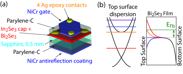
No previous optical probe has been reported that attempts to measure the quantized Hall effect on a topological insulator as a function of gate voltage.Jenkins et al. (2012); Jenkins et al. (2010a); Sushkov et al. (2010); Brune et al. (2011); Hancock et al. (2011); Kvon et al. (2012); Schafgans et al. (2012); Valdes Aguilar et al. (2012) We report Faraday angle and transmission measurements performed at a fixed laser frequency of THz as a function of gate voltage at discrete magnetic fields up to T on two topological insulating films. These Bi2Se3 thin films, and quintuple layers thick (1 QL 1 nm), were grown epitaxially onto mm thick sapphire substrates and capped with nm thick In2Se3 layers without breaking vacuum.Bansal et al. (2011a, b) As depicted in Figure 1(a), the dielectric Parylene-C was deposited encasing the sample to a thickness of nm ( nm) for the 60 (40) QL film. A NiCr top gate and a NiCr antireflection coating were evaporated onto the Parylene-C. For the 60 QL device, the gate moves a charge density of per volt on or off the Bi2Se3 film.
The Faraday angle is related to the off-axis conductivity of a thin film by where , and is the substrate index of refraction, is the impedance of free space, and is the longitudinal conductivity.Jenkins et al. (2010b); Jenkins et al. (2012) Considering the case where the cyclotron frequency is large compared to the scattering rate and radiation frequency , and is small compared with , crossing a Landau level results in . Under very specific geometric conditions, the substrate properties can be ignored and is quantized exactly in units of .O’Connell and Wallace (1982); Volkov and Mikhailov (1985); Maciejko et al. (2010); Tse and MacDonald (2010) More generally, the quantization of from step-to-step is scaled by the material properties of the substrate and any longitudinal conductivity contributions (like a conducting gate or other dissipation channels), as well as corrections from non-zero and .Morimoto et al. (2009); Stier et al. (2011)
The complex Faraday angle measurement at THz frequencies utilizes polarization-modulated fixed-frequency laser radiation, a technique detailed elsewhere.Jenkins et al. (2010b) The beam is normally incident on the film held at K that is maintained in a normally applied magnetic field. The transmission through the film is measured concurrently. The differential Faraday angle and the differential transmission are differences between the optical signals measured at a fixed gate voltage V and the signals measured at a variable gate voltage .
The differential Faraday angle and differential transmission as a function of gate voltage at fixed fields for the two devices are reported in Figure 2. Measurements performed at THz frequencies on the same 60 quintuple layer (QL) device, but as a function of magnetic field, are reported in reference 8. The gate sweeps at fixed magnetic field presented here offer better signal-to-noise than previous measurements. is measured to within a standard deviation of the mean of rad without systematic drift effects associated with changing the magnetic field. With this additional sensitivity, of the QL film shows an extraordinarily flat response over a tremendous span of gate voltages, from V to V.
The previous THz measurements on the 60 QL film provide an overview of the characteristics of the film. The salient features of the THz data are captured utilizing two gate dependent Drude terms in the conductivity: the first term is primarily associated with the bulk carriers of the gate-modulated screened region near the top surface (MTB), and the second term is the top topological surface state (TSS). The conception of the model is based upon the Thomas-Fermi band bending in the film, depicted in Figure 1(b). All carrier contributions in the film were measured to be n-type. Based on the small measured cyclotron mass at high negative gate voltages, the Dirac point is estimated to be in the vicinity of V. The conduction band edge (CBE) voltage location is V deduced from a sudden increase in the measured surface state scattering rate, interpreted as the optical signature where surface state carriers begin scattering into bulk channels, and is demarcated by the green vertical dashed lines in Figure 2.Jenkins et al. (2012) This corresponds to a CBE that is 80 meV above the Dirac point, whereas the vacuum/Bi2Se3 interface CBE characterized by surface probes is at 190 meVXia et al. (2009); Zhu et al. (2011); Bahramy et al. (2012) implying a shift in the Dirac point due to the In2Se3/Bi2Se3 interface properties.Jenkins et al. (2012) With regard to the plateau region, this is a minor point since top surface bulk carriers are degenerate with the surface state carriers over the full range of the plateau whether the CBE location is 80 or 190 meV above the Dirac point (as discussed in more detail in the Appendix).
There are a number of important observations associated with the plateau in the shown in Figure 2(a) and (g). The first is the degree of flatness. Such an extremely flat response is very difficult to reproduce invoking non-quantized behavior. In the simplest view, a gate moves electrons to the film with increasingly positive gate voltage, predictably lowering the transmission as reported in Figure 2(c), yet the real part of the Faraday angle remains constant over a large range of voltages.
A slightly more sophisticated approach using the same multi-fluid Drude model that reproduced the features of all the data reported in reference 8 does not reproduce the extremely flat behavior of the gate sweeps in fixed magnetic field, as shown in Figure 2(i). The gate dependent scattering rates of the TSS and MTB Drude terms give rise to an extremum in the modelled response of Figure 2(i). The observation in Figure 2(g) of such a flat response over such a large range of gate voltages is irreconcilable with two gate-dependent n-type Drude terms while maintaining consistency with previous optical data. The data suggests the existence of localized states associated with which absorb the transferred charge from the gate but give no additional contribution to .
The formation of Landau levels is one way that can provide localized states. Although we currently do not have a complete explanation for the observed plateau, recent dc Hall measurements on highly doped cm-3 Bi2Se3 bulk crystals, performed on many different samples spanning four orders of magnitude in thickness, appear to support the scenario that an extraordinary bulk quantum Hall effect (QHE) occurs in which each pair of QLs contribute a distinct Landau Level to the Hall response.Cao et al. (2012) These Landau levels appear to act in unison such that the step-to-step height . However, oscillates but does not go to zero, remaining comparable with even within plateaus, indicating appreciable dissipation. Within this context, we discuss the character of the observed plateau in the shown in Figure 2(g).
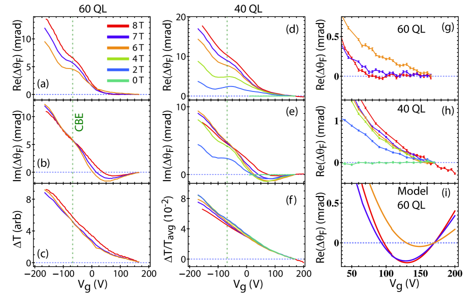
For small longitudinal conductivity ( and large cyclotron frequency , the finite-frequency off-axis conductivity reduces to since the spectral weight and the cyclotron frequency . The electron density changes by when the Fermi level sweeps through a single Landau Level at fixed magnetic field , so . Since sapphire has an index of refraction of , for the NiCr gate, and , the change in the real part of the Faraday angle upon stepping through a Landau Level is expected to be mrad in the low frequency limit. In this limit, the at T is flat over a range of at least V to within 1/80 of the expected step size from a single Landau level. The expected step size for a 2DEG has been predicted to increase from this estimate due to the finite probe frequency ( THz) and scattering rate ( THz) in comparison to the cyclotron frequency ( THz at T).Morimoto et al. (2009)
The plateau at positive gate voltage decreases in width with decreasing magnetic field qualitatively consistent with Landau level behavior. The surface state is degenerate with surface accumulated bulk carriers over the full range of the plateau. The step-like feature at V at the CBE location is a result of the changing surface state scattering rate.Jenkins et al. (2012) This feature does not display the expected behavoir by a quantized Hall step upon changing the magnetic field.
The width of the positive-voltage plateau is much larger than expected from a single Landau level. The gate moves /cm2 over V, and each Landau level is occupied by an electron density of cm-2 in T. At least Landau levels are traversed over the span of the plateau.
Given that no Landau level steps are discernable in the data at negative gate voltages, and the topological surface state is singly occupied contributing at most 1 Landau level of charge, the conclusion is that the plateau must primarily be a bulk effect.
Figure 2(d-f) and (h) show gated THz measurements performed on a 40 QL Bi2Se3 film. Although the qualitative behavior is very similar to the 60 QL film, there are no plateaus in the response. The Thomas-Fermi screening length is estimated to be about nm based upon dc measurements of bulk densities of similarly prepared films performed over a wide range of thicknesses (see Appendix). Gating the top surface of the nm film will affect the accumulated bottom surface layer much more than the thicker nm film. An additional gate dependent conductivity channel associated with the bottom surface accumulation layer can give rise to a different behavior. Study of thicker films is necessary to verify this thickness effect.
The gate dependence of and Im() of the 60 QL film over the same voltage range where the plateau exists indicates dissipation in the and channels. In this regard, the similarities between the reported dc measured bulk QHECao et al. (2012) and the gated THz measurements are striking. These dc data show plateaus in the Hall conductivity, consistent with the sum of many Landau level contributions, in the presence of significant dissipative channels.
However, even the highest positive applied gate voltage of V, which causes the conduction band to bend downward at the surface as depicted in Figure 1(b), only results in a Fermi level of meV above the conduction band edge at the surface (see Appendix). This Fermi level translates into a bulk density of cm-3, about an order of magnitude less than the dc measurements on bulk crystals reporting bulk QHE.Cao et al. (2012)
More important, the most significant difference between the THz and dc experiments is associated with the gradient of the potential from band bending effects in the film produced by the applied gate. In the case of the dc measurements, identical independent two-dimensional layers exhibiting the QHE are known to summate in the expected way, corresponding to a single Landau level but with a degeneracy corresponding to the number of layers.Haavasoja et al. (1984) However, if the potential varies appreciably from layer to layer, the Landau levels would not remain degenerate nor give well defined large steps. In our case, screening effects are expected to cause such a misalignment of Landau levels. At V, the bands are bent downward by meV over QL (the screening length), producing meV change in potential energy from QL to QL. The Landau level spacing (cyclotron frequency) in T is only meV, so one might expect the variation of potential would wipe out any additive effect from independent Landau levels that could produce a wide Hall plateau.
This may indicate that the contributing Landau levels are not independent, but interact in a way that tends to lock the levels together. For the dc measured bulk QHE of reference 31, the scenario put forth was that the quintuple layers of Bi2Se3 decouple, forming independent 2-DEGs. Many questions remain about the nature of this decoupling since Shubnikov-de Haas measurements show a 3-D Fermi surface.Kohler (1973); Eto et al. (2010) It is also puzzling how the QHE survives the large measured in the Hall plateaus.Cao et al. (2012) Similarly in this paper we report the phenomenology of an extremely flat Hall response observed at sub-THz frequencies, manifesting in the real part of the Faraday angle that is flat to within 1/80 of the expected low-frequency quantized step size for a single Landau level. This plateau extends over a large range of gate induced carrier density change of , occurring above the conduction band edge, corresponding to more than occupied Landau levels. A full understanding of this plateau is likely tied to understanding the bulk QHE, which currently remains elusive.
The authors thank M. S. Fuhrer, T. D. Stanescu, and S. Das Sarma for helpful conversations. The work at the University of Maryland is supported by NSF (DMR-1104343) and CNAM. The Rutgers work is supported by IAMDN of Rutgers University, National Science Foundation (NSF DMR-0845464,) and Office of Naval Research (ONR N000140910749).
Appendix
The following is a summary of characterization results of the 60 nm film stated in the main text. This particular 60 nm film has been extensively characterized spectroscopically in reference 8. Results directly obtained from raw optical data in reference 8 and dc transport measurements on similarly grown films in reference 16, used in conjunction with Thomas-Fermi screening, provide important information of the carriers involved in the gated Faraday angle response in the plateau region.
DC transport measurements on uncapped films, grown in exactly the same manner as our film but without a capping layer, show a carrier density cm-2 over a wide range of film thicknesses. The thickness independence of the carrier density indicates the bulk contribution is small compared to the two accumulated surfaces (topological surface states and bulk accumulation layers). The bulk carrier density is measured to be cm-3.Bansal et al. (2011a) The cyclotron mass is m0 (taken directly from the THz Faraday and cyclotron resonance data).Jenkins et al. (2012) The screening length depends weakly on bulk density, so it is nm. The bulk density corresponds to a bulk Fermi level of meV.
For comparison, this bulk carrier density distributed uniformly over a nm film results in a 2-D carrier density of only cm-2. A single-fluid fit to zero-gate FTIR data and Faraday angle give the total carrier density in the film, cm-2.Jenkins et al. (2012)
A very small cyclotron mass measured in the gate-modulated THz cyclotron resonance (-CR) data at high negative gate voltage is obtained directly from the raw data in Figure 2(a) of reference 8. Such a small mass is direct evidence of the topological surface state. An immediate consequence is that the Fermi level in the surface state is very near the Dirac point at V. At this voltage, a depletion region necessarily exists at the top surface as indicated by the red curve in Figure 1(b) of the main text.
A bulk density of cm-3 is consistent with dc characterizationsBansal et al. (2011a) and optical characterizations.Jenkins et al. (2012) At V, the Dirac cone is empty and there is a depletion layer of charge in the film. The gate is capable of moving carriers for a change in gate voltage . The conduction band is reached when the gate supplies enough charge to fill both the surface state () up to the conduction band edge as well as the depletion charge, or . This condition is depicted by the orange curve in Figure 1.
The depletion charge is calculated by solving the Thomas-Fermi screening model, giving , where is the energy of the conduction band edge above the Dirac point. From the ARPES measured surface state, is given by the average dispersion .Jenkins et al. (2012)
For a conduction band edge that is 190 meV above the Dirac point, cm-2 and cm-2. The surface Fermi level will equal the conduction band edge, therefore, when V. If the gate changes another 100 V to V, the top surface becomes accumulated, as depicted in purple in Figure 1.
Optical characterizations of the 60 nm film show evidence that the conduction band edge is at -70 V, as mentioned in the main text. Since the Dirac point is at -170 V, the number of carriers transferred by the gate is cm-2. Solving gives meV where cm-2 and cm-2. To then change the gate to V will transfer an additional cm-2 carriers to the film. Over the entire voltage range in which the plateau is gated, the top surface bulk is accumulated. The resulting surface Fermi level at V is meV above the conduction band edge, found from solving the Thomas-Fermi screening model (a method that is derived in detail in reference 8 in the Supplemental Materials, Section II).
In either case, whether the conduction band edge is located at 190 meV or 80 meV above the Dirac point, there are bulk carriers that are degenerate with surface state carriers over the full range of the observed plateau.
Also, a bottom surface accumulation layer exists in both these cases. From V to , cm-2 carriers are added to the film filling the depletion layer and transferring carriers into the surface state and bulk. Therefore, the net carrier density at the top surface is . In both cases, the net carrier density at the top surface is cm-2. The remaining cm-2 carriers optically characterized by zero-gate measurementsJenkins et al. (2012) are in the bottom surface and bulk. The bulk is a small contribution, implying that the bottom surface is accumulated.
References
- Volkov and Mikhailov (1985) V. A. Volkov and S. A. Mikhailov, JETP Letters 41, 389 (1985).
- Hasan and Kane (2010) M. Z. Hasan and C. L. Kane, Reviews of Modern Physics 82, 3045 (2010).
- Qi and Zhang (2011) X.-L. Qi and S.-C. Zhang, Reviews of Modern Physics 83, 1057 (2011).
- Maciejko et al. (2010) J. Maciejko, X.-L. Qi, H. D. Drew, and S.-C. Zhang, Physical Review Letters 105, 166803 (2010).
- Tse and MacDonald (2010) W.-K. Tse and A. H. MacDonald, Physical Review Letters 105, 057401 (2010).
- Wilczek (1987) F. Wilczek, Physical Review Letters 58, 1799 (1987), URL http://link.aps.org/doi/10.1103/PhysRevLett.58.1799.
- Qi et al. (2008) X.-L. Qi, T. L. Hughes, and S.-C. Zhang, Physical Review B 78, 195424 (2008).
- Jenkins et al. (2012) G. S. Jenkins, A. B. Sushkov, D. C. Schmadel, M. Bichler, G. Koblmueller, M. Brahlek, N. Bansal, S. Oh, and H. D. Drew, arXiv:1208.3881 (2012), URL http://arxiv.org/abs/1208.3881.
- Jenkins et al. (2010a) G. S. Jenkins, A. B. Sushkov, D. C. Schmadel, N. P. Butch, P. Syers, J. Paglione, and H. D. Drew, Physical Review B 82, 125120 (2010a).
- Butch et al. (2010) N. P. Butch, K. Kirshenbaum, P. Syers, A. B. Sushkov, G. S. Jenkins, H. D. Drew, and J. Paglione, Physical Review B 81, 241301 (2010).
- Kong et al. (2011) D. Kong, J. J. Cha, K. Lai, H. Peng, J. G. Analytis, S. Meister, Y. Chen, H.-J. Zhang, I. R. Fisher, Z.-X. Shen, et al., ACS Nano 5, 4698 (2011).
- Checkelsky et al. (2011) J. G. Checkelsky, Y. S. Hor, R. J. Cava, and N. P. Ong, Physical Review Letters 106, 196801 (2011).
- Analytis et al. (2010) J. G. Analytis, R. D. McDonald, S. C. Riggs, J.-H. Chu, G. S. Boebinger, and I. R. Fisher, Nature Physics 6, 960 (2010).
- Steinberg et al. (2010) H. Steinberg, D. R. Gardner, Y. S. Lee, and P. Jarillo-Herrero, Nano Letters 10, 5032 (2010).
- Kim et al. (2012) D. Kim, S. Cho, N. P. Butch, P. Syers, K. Kirshenbaum, S. Adam, J. Paglione, and M. S. Fuhrer, Nature Physics 8, 460 (2012).
- Bansal et al. (2011a) N. Bansal, Y. S. Kim, M. Brahlek, E. Edrey, and S. Oh, arXiv:1104.5709 (2011a).
- Sushkov et al. (2010) A. B. Sushkov, G. S. Jenkins, D. C. Schmadel, N. P. Butch, J. Paglione, and H. D. Drew, Physical Review B 82, 125110 (2010).
- Brune et al. (2011) C. Brune, C. X. Liu, E. G. Novik, E. M. Hankiewicz, H. Buhmann, Y. L. Chen, X. L. Qi, Z. X. Shen, S. C. Zhang, and L. W. Molenkamp, Physical Review Letters 106, 126803 (2011).
- Hancock et al. (2011) J. N. Hancock, J. L. M. van Mechelen, A. B. Kuzmenko, D. van der Marel, C. Brüne, E. G. Novik, G. V. Astakhov, H. Buhmann, and L. Molenkamp, 1105.0884 (2011), URL http://arxiv.org/abs/1105.0884.
- Kvon et al. (2012) Z. Kvon, S. Danilov, D. Kozlov, C. Zoth, N. Mikhailov, S. Dvoretskii, and S. Ganichev, JETP Letters 94, 816–819 (2012).
- Schafgans et al. (2012) A. A. Schafgans, K. W. Post, A. A. Taskin, Y. Ando, X.-L. Qi, B. C. Chapler, and D. N. Basov, Physical Review B 85, 195440 (2012).
- Valdes Aguilar et al. (2012) R. Valdes Aguilar, A. V. Stier, W. Liu, L. S. Bilbro, D. K. George, N. Bansal, L. Wu, J. Cerne, A. G. Markelz, S. Oh, et al., Physical Review Letters 108, 087403 (2012).
- Bansal et al. (2011b) N. Bansal, Y. S. Kim, E. Edrey, M. Brahlek, Y. Horibe, K. Iida, M. Tanimura, G.-H. Li, T. Feng, H.-D. Lee, et al., Thin Solid Films 520, 224 (2011b).
- Jenkins et al. (2010b) G. S. Jenkins, D. C. Schmadel, and H. D. Drew, Review of Scientific Instruments 81, 083903 (2010b).
- O’Connell and Wallace (1982) R. F. O’Connell and G. Wallace, Physical Review B 26, 2231 (1982).
- Morimoto et al. (2009) T. Morimoto, Y. Hatsugai, and H. Aoki, Physical Review Letters 103, 116803 (2009).
- Stier et al. (2011) A. V. Stier, H. Zhang, C. T. Ellis, D. Eason, G. Strasser, T. Morimoto, B. D. McCombe, H. Aoki, and J. Cerne, arXiv:1201.0182 (2011), URL http://arxiv.org/abs/1201.0182.
- Xia et al. (2009) Y. Xia, D. Qian, D. Hsieh, L. Wray, A. Pal, H. Lin, A. Bansil, D. Grauer, Y. S. Hor, R. J. Cava, et al., Nature Physics 5, 398 (2009).
- Zhu et al. (2011) Z.-H. Zhu, G. Levy, B. Ludbrook, C. N. Veenstra, J. A. Rosen, R. Comin, D. Wong, P. Dosanjh, A. Ubaldini, P. Syers, et al., Physical Review Letters 107, 186405 (2011).
- Bahramy et al. (2012) M. S. Bahramy, P. D. C. King, A. de la Torre, J. Chang, M. Shi, L. Patthey, G. Balakrishnan, P. Hofmann, R. Arita, N. Nagaosa, et al., arXiv:1206.0564 (2012), URL http://arxiv.org/abs/1206.0564.
- Cao et al. (2012) H. Cao, J. Tian, I. Miotkowski, T. Shen, J. Hu, S. Qiao, and Y. P. Chen, Physical Review Letters 108, 216803 (2012).
- Haavasoja et al. (1984) T. Haavasoja, H. Stormer, D. Bishop, V. Narayanamurti, A. Gossard, and W. Wiegmann, Surface Science 142, 294–297 (1984).
- Kohler (1973) H. Kohler, physica status solidi (b) 58, 91–100 (1973).
- Eto et al. (2010) K. Eto, Z. Ren, A. A. Taskin, K. Segawa, and Y. Ando, Physical Review B 81, 195309 (2010).