Hard superconducting gap in PbTe nanowires
Abstract
Semiconductor nanowires coupled to a superconductor provide a powerful testbed for quantum device physics such as Majorana zero modes and gate-tunable hybrid qubits. The performance of these quantum devices heavily relies on the quality of the induced superconducting gap. A hard gap, evident as vanishing subgap conductance in tunneling spectroscopy, is both necessary and desired. Previously, a hard gap has been achieved and extensively studied in III-V semiconductor nanowires (InAs and InSb). In this study, we present the observation of a hard superconducting gap in PbTe nanowires coupled to a superconductor Pb. The gap size () is 1 meV (maximally 1.3 meV in one device). Additionally, subgap Andreev bound states can also be created and controlled through gate tuning. Tuning a device into the open regime can reveal Andreev enhancement of the subgap conductance, suggesting a remarkable transparent superconductor-semiconductor interface, with a transparency of 0.96. These results pave the way for diverse superconducting quantum devices based on PbTe nanowires.
A superconductor can induce superconductivity in a semiconductor through proximity coupling. This coupling was spatially non-uniform in early devices due to disorder at the semiconductor-superconductor interface [1]. While supercurrent can still be clearly resolved in Josephson devices [2], the induced superconducting gap was soft with many quasi-particle states inside the gap. The soft gap can significantly degrade the quality of the corresponding device [3], through mechanisms such as dissipation smearing or quasi-particle poisoning. Semiconductor nanowires provide a natural platform to study the induced superconducting gap, where an electrostatic gate can readily define a point contact for tunneling spectroscopy. The tunneling conductance reflects the density of states and can thus be associated with the quality of the induced superconducting gap. The issue of a soft gap in semiconductor nanowires can be addressed by suppressing interface disorder [4, 5]. Furthermore, epitaxial growth of superconductors can yield atomically sharp interfaces and hard gaps [6, 7, 8, 9]. These material improvements enable high quality quantum devices, e.g. on Majorana experiments [10, 11, 12, 13, 14, 15, 16, 17, 18] and hybrid qubits [19, 20, 21, 22, 23, 24]. So far, most of the hard gap studies are based on III-V semiconductors such as InAs or InSb. The Majorana theory [25, 26] requires a clean semiconductor nanowire while the current experiments are disorder-limited [27, 28, 29, 30, 31].
PbTe nanowires have been recently proposed [32] to overcome the disorder issue, owing to their large dielectric constant ( 1350). Meanwhile, these nanowires have been grown using selective area epitaxy [33, 34] and subjected to quantum transport characterization [35, 36, 37]. The superconducting proximity effect has also been demonstrated in PbTe-Pb Josephson junctions [38]. While a superconducting gap with a size of 0.4 meV can be inferred, it is essential to note that tunneling spectroscopy in a Josephson device does not directly unveil the quasi-particle density of states (DOS) but rather a convolution of them. Moreover, the subgap conductance may have other contributions from the supercurrent and multiple Andreev reflections. Therefore, to directly probe the induced gap, N-NW-S devices are needed (where N stands for normal metal, NW for nanowire and S for superconductor). We have recently improved the material quality and here demonstrate the hard superconducting gap in PbTe nanowires in N-NW-S devices. We used Pb as the superconductor and measured a superconducting gap of 1 meV. This value is comparable to those observed in InAs-Pb devices [39] and significantly larger than those reported in our early devices [38]. The transparency, estimated based on the Andreev enehancement in the open regime, can reach 0.96, also significantly higher than before ( 0.8) [38]. Andreev bound states (ABSs) can be generated and controlled by gate voltages, providing an additional material platform for investigating Andreev physics. These results are a pivotal advancement in utilizing PbTe nanowires for advanced quantum devices.
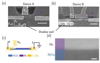
Figures 1(a) and 1(b) depict scanning electron micrographs (SEMs) of two devices (A and B). The PbTe nanowires were grown on a CdTe(001)/Pb1-xEuxTe substrate, and subsequently covered epitaxially with a thin Pb film (thickness 10 nm) and a CdTe capping layer. The value of is estimated to be 0.01. The substrate was cooled using liquid nitrogen during the Pb growth process. The Pb film on the substrate of device B is discontinuous, likely due to the relatively high temperature during that particular growth. Nonetheless, the Pb films on the PbTe nanowires in both devices are uniform and continuous. The barrier region of the nanowire is defined by pre-patterned Hydrogen SilsesQuioxane (HSQ) shadow wall. The barrier transmission can be tuned by applying a voltage () to the side gate. The source and drain contacts, along with the side gates, were fabricated using evaporated Ti/Au (7/60 nm). Details of device fabrication can be found in the method section. Standard two-terminal measurement was performed in a dilution fridge at its base temperature (below 50 mK). Figure 1(c) shows a simplified circuit and the schematic of the N-NW-S device. The scanning transmission electron microscopy (STEM) image in Fig. 1(d) displays a PbTe-Pb interface that was grown under identical conditions. An atomically sharp interface is crucial for the observation of a hard induced gap.
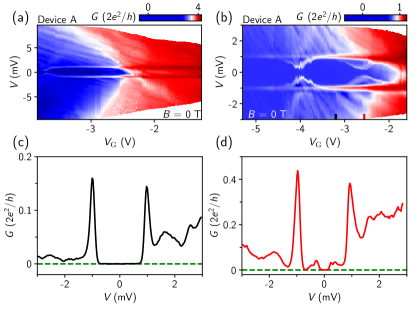
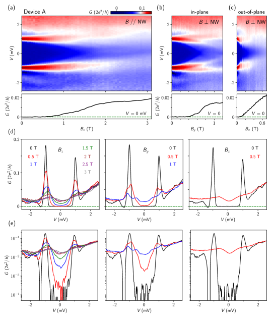
Figure 2(a) illustrates the conductance spectroscopy of device A over a large bias () range. The magnetic field () was kept at zero. The differential conductance, , was acquired using the standard lock-in technique. Note that the line resistance, mainly contributed by the fridge filters, has been subtracted from . Additionally, has also been corrected by subtracting the bias drop over the line resistance. The two horizontal lines near mV are the coherence peaks that feature the edges of the superconducting gap. To better resolve the gap, Fig. 2(b) shows a fine scan over a smaller range. More negative depletes the barrier region and pinches off the device. Near the pinch-off regime, the tunneling conductance is proportional to the DOS of the proximitized PbTe. The line cut (Fig. 2(c)) shows sharp coherence peaks and vanishing sub-gap conductance, indicating a hard superconducting gap. The suppression of conductance (outside-gap vs sub-gap) can reach two orders of magnitude, see Fig. S1 for the log-scale plot in the Supplemental Material. The bias values of the coherence peaks suggest a gap size 1 meV, significantly larger than that of Al ( 0.20.3 meV). A large superconducting gap is favorable for Majorana research as it sets an upper limit for the size of the topological gap. Larger gap can “tolerate” stronger disorder. Compared to the previous work on InAs-Pb nanowires [39], the gap size is similar but the coherence peaks here seem more sharply defined. Sharper coherence peaks suggest less dissipation smearing arising from undesirable quasi-particles [40].
Besides the hard gap, another notable feature is the discrete sub-gap levels at particular gate voltages. These gate-tunable levels are ABSs, revealed as sub-gap conductance peaks (see Fig. 2(d) for a line cut). ABSs are widely present in hybrid devices [41, 42, 43, 44, 45] and can mimic Majorana signatures, causing the decade-long debate [46, 47, 48, 49, 50, 51, 52]. ABSs usually originate in quantum dots coupled to superconductors. Figures 2(a-b) show no obvious Coulomb blockades except for single resonant levels near = -4 V and = -2.5 V. The white boundaries demarcating the red and blue regions in the color map suggest diamond like shapes, see the dashed lines in Fig. S1(a). These diamonds are unlikely to be Coulomb blockades, considering that the charging energy in PbTe should be two orders of magnitude smaller [36]. The diamond slopes likely correspond to the subband bottoms of a quantum point contact [37]. In Fig. S1 we show possible indication of quasi-ballistic transport after moderate smoothing on Fig. 2(a). In the absence of quantum dots, the observed ABSs are likely formed due to the smooth potential variation [46, 47].
The outside-gap conductance exhibits Fabry-Perot-like oscillations over , possibly caused by the scattering between the barrier region and the drain contact. These oscillations can affect the estimation of the normal state conductance (). In Fig. S1, we present the extracted plotted against , i.e. . We also compare it with the BTK-Beenakker formula [53, 54] for illustrative purposes. Deviation between the formula and experiment exist and may arise from various factors. Firstly, the aforementioned oscillations make the estimation of inaccurate. Secondly, the gap size of 1 meV is a significant fraction of the subband spacing in PbTe [37]. Unlike the scenario of Al with a much smaller gap, the outside-gap (large-bias) conductance in PbTe-Pb may not accurately reflect the barrier transmission (normal state conductance) at zero bias. Lastly, a crucial factor is that the BTK-Beenakker formula assumes a single channel in the barrier, which may not always hold. Moreover, even for the single channel case, the formula only holds for high chemical potentials [55], thus has limited implications.
We next study the dependence of the hard gap (for the dependence of ABSs, see Fig. S2 in the Supplemental Material). Figures 3(a-c) show the scans along three coordinate axes, see Fig. 1(a) for the labeling. is roughly parallel to the nanowire (with an accuracy within 10∘). The gap becomes soft for approaching 1 T, see the lower panel for the zero-bias line cut. The gap closes as approaches 2 T. The other two directions, (in-plane) and (out-of-plane), are both perpendicular to the nanowire. In the scan, the gap closes at a lower field ( 1 T) than the case, while in the scan, an even lower field ( 0.5 T) is sufficient to close the gap. We attribute the gap closing in the scan to the orbital effect, given that is perpendicular to the Pb film. As for and , the orbital effect is smaller, as both directions are in-plane (parallel to the Pb film). We ascribe the anisotropy between and to spin-orbit interaction. aligns with the nanowire, therefore is perpendicular to the spin-orbit direction (). Spin-orbit interaction protects the gap from closing when is perpendicular to , thus a higher critical field is observed for . is parallel to . Hence the gap closes without the protection and a lower critical field is observed. This spin-orbit-induced anisotropy has been previously demonstrated in InSb nanowires coupled to a superconductor NbTiN [56].
Figures 3(d) and 3(e) illustrate line cuts at different fields in linear and logarithmic scales for these three directions to further illustrate this anisotropy. At zero field, the gap shows a conductance suppression over two orders of magnitude. At 0.5 T (the red curves), the gap still remains hard in the scan while the sub-gap conductance has already been increased by an order of magnitude in the scan and by two orders of magnitude in the scan. In Fig. S3 in the Supplemental Material, we present a similar anisotropy observed in another device. Note that in the InAs-Pb work [39], the hard gap can persist to a considerable higher ( 8.5 T). Further increasing the critical field for PbTe nanowires should be achievable and can be a topic for our forthcoming optimization efforts.
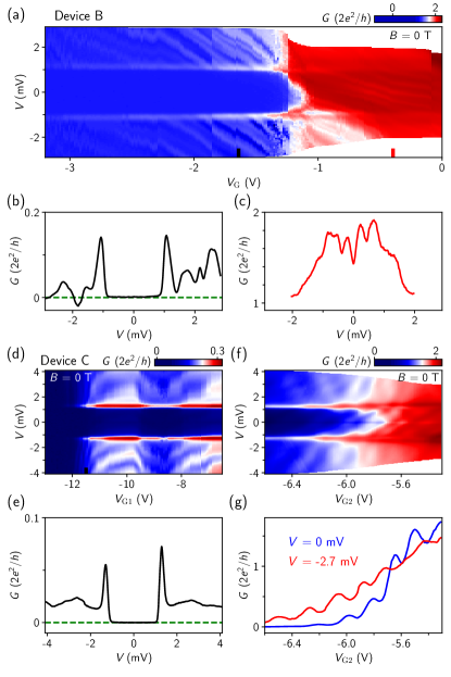
For reproducibility purpose, we present two additional devices (B and C) in Fig. 4 demonstrating hard gaps. One more device (device D) can also be found in Fig. S3. Figure 4(a) shows the conductance map of device B. In the tunneling regime, a gap of 1.05 meV is observed, see Fig. 4(b) for a line cut. The negative differential conductance outside the gap (near the coherence peak) is typical in nanowire hybrids with discrete energy levels [4]. In the open regime where the outside-gap conductance is close to , the subgap conductance is enhanced relative to the outside-gap conductance, as shown Fig. 4(c). This enhancement is due to Andreev reflection. The enhancement factor is 1.7. Using the BTK-Beenakker formula [53, 54], we can estimate the interface transparency 0.96.
Device C is an island device [57] but operated as a tunneling spectroscopy device by setting one barrier region to be open (conductance much larger than ). A hard gap with sharp coherence peaks can be observed in Figs. 4(d-e). The gap size is 1.3 meV. For all devices (A, B, C and D), Fabry-Perot-like oscillations outside the gap are present. The oscillations for subgap conductance becomes noticeable in a more opened regime as shown in Figs. 4(f-g) for device C. The quasi-periodic oscillations suggest two well-defined scattering points, likely the two barrier regions of the island device. Note that even if one barrier is tuned to be considerably open, it can still act as a scattering point in Fabry-Perot oscillations.
In summary, we have observed a hard superconducting gap with sharp coherence peaks in PbTe nanowires coupled to a superconductor Pb. The gap size is 1 meV, several times larger than that of Al. Our result may enable the search for high quality Majorana signatures in PbTe nanowires, as well as other PbTe-based hybrid superconducting quantum devices.
Acknowledgment This work is supported by Tsinghua University Initiative Scientific Research Program, National Natural Science Foundation of China (92065206) and the Innovation Program for Quantum Science and Technology (2021ZD0302400). Raw data and processing codes within this paper are available at https://doi.org/10.5281/zenodo.8313595.
References
- Takei et al. [2013] S. Takei, B. M. Fregoso, H.-Y. Hui, A. M. Lobos, and S. D. Sarma, Soft superconducting gap in semiconductor Majorana nanowires, Physical Review Letters 110, 186803 (2013).
- Doh et al. [2005] Y.-J. Doh, J. A. van Dam, A. L. Roest, E. P. A. M. Bakkers, L. P. Kouwenhoven, and S. D. Franceschi, Tunable supercurrent through semiconductor nanowires, Science 309, 272 (2005).
- Mourik et al. [2012] V. Mourik, K. Zuo, S. M. Frolov, S. Plissard, E. P. Bakkers, and L. P. Kouwenhoven, Signatures of Majorana fermions in hybrid superconductor-semiconductor nanowire devices, Science 336, 1003 (2012).
- Gül et al. [2017] Ö. Gül, H. Zhang, F. K. de Vries, J. van Veen, K. Zuo, V. Mourik, S. Conesa-Boj, M. P. Nowak, D. J. van Woerkom, M. Quintero-Pérez, et al., Hard superconducting gap in InSb nanowires, Nano Letters 17, 2690 (2017).
- Zhang et al. [2017] H. Zhang, Ö. Gül, S. Conesa-Boj, M. P. Nowak, M. Wimmer, F. K. De Vries, J. Van Veen, M. W. De Moor, et al., Ballistic superconductivity in semiconductor nanowires, Nature Communications 8, 16025 (2017).
- Chang et al. [2015] W. Chang, S. Albrecht, T. Jespersen, F. Kuemmeth, P. Krogstrup, J. Nygård, and C. M. Marcus, Hard gap in epitaxial semiconductor–superconductor nanowires, Nature Nanotechnology 10, 232 (2015).
- Krogstrup et al. [2015] P. Krogstrup, N. Ziino, W. Chang, S. Albrecht, M. Madsen, E. Johnson, J. Nygård, C. Marcus, and T. Jespersen, Epitaxy of semiconductor–superconductor nanowires, Nature Materials 14, 400 (2015).
- Zellekens et al. [2020] P. Zellekens, R. Deacon, P. Perla, H. A. Fonseka, T. Mörstedt, S. A. Hindmarsh, B. Bennemann, F. Lentz, M. I. Lepsa, A. M. Sanchez, et al., Hard-gap spectroscopy in a self-defined mesoscopic / nanowire josephson junction, Phys. Rev. Appl. 14, 054019 (2020).
- Pan et al. [2022] D. Pan, H. Song, S. Zhang, L. Liu, L. Wen, D. Liao, R. Zhuo, Z. Wang, Z. Zhang, S. Yang, J. Ying, W. Miao, R. Shang, H. Zhang, and J. Zhao, In situ epitaxy of pure phase ultra-thin InAs-Al nanowires for quantum devices, Chinese Physics Letters 39, 058101 (2022).
- Deng et al. [2016] M. Deng, S. Vaitiekėnas, E. B. Hansen, J. Danon, M. Leijnse, K. Flensberg, J. Nygård, P. Krogstrup, and C. M. Marcus, Majorana bound state in a coupled quantum-dot hybrid-nanowire system, Science 354, 1557 (2016).
- Gül et al. [2018] Ö. Gül, H. Zhang, J. D. Bommer, M. W. de Moor, D. Car, S. R. Plissard, E. P. Bakkers, A. Geresdi, K. Watanabe, T. Taniguchi, et al., Ballistic Majorana nanowire devices, Nature Nanotechnology 13, 192 (2018).
- Song et al. [2022] H. Song, Z. Zhang, D. Pan, D. Liu, Z. Wang, Z. Cao, L. Liu, L. Wen, D. Liao, R. Zhuo, D. E. Liu, R. Shang, J. Zhao, and H. Zhang, Large zero bias peaks and dips in a four-terminal thin InAs-Al nanowire device, Phys. Rev. Research 4, 033235 (2022).
- Wang et al. [2022a] Z. Wang, H. Song, D. Pan, Z. Zhang, W. Miao, R. Li, Z. Cao, G. Zhang, L. Liu, L. Wen, R. Zhuo, D. E. Liu, K. He, R. Shang, J. Zhao, and H. Zhang, Plateau regions for zero-bias peaks within 5 of the quantized conductance value , Phys. Rev. Lett. 129, 167702 (2022a).
- Dvir et al. [2023] T. Dvir, G. Wang, N. Loo, C.-X. Liu, G. Mazur, A. Bordin, S. Haaf, J.-Y. Wang, D. Driel, F. Zatelli, et al., Realization of a minimal Kitaev chain in coupled quantum dots, Nature 614, 445 (2023).
- Aghaee et al. [2023] M. Aghaee, A. Akkala, Z. Alam, R. Ali, A. Alcaraz Ramirez, M. Andrzejczuk, A. E. Antipov, P. Aseev, M. Astafev, B. Bauer, et al. (Microsoft Quantum), Inas-al hybrid devices passing the topological gap protocol, Phys. Rev. B 107, 245423 (2023).
- Zhang et al. [2019] H. Zhang, D. E. Liu, M. Wimmer, and L. P. Kouwenhoven, Next steps of quantum transport in Majorana nanowire devices, Nature Communications 10, 5128 (2019).
- Prada et al. [2020] E. Prada, P. San-Jose, M. W. de Moor, A. Geresdi, E. J. Lee, J. Klinovaja, D. Loss, J. Nygård, R. Aguado, and L. P. Kouwenhoven, From Andreev to Majorana bound states in hybrid superconductor–semiconductor nanowires, Nature Reviews Physics 2, 575 (2020).
- Cao et al. [2023] Z. Cao, S. Chen, G. Zhang, and D. E. Liu, Recent progress on Majorana in semiconductor-superconductor heterostructures–engineering and detection, Sci. China-Phys. Mech. Astron. 66, 267003 (2023).
- Larsen et al. [2015] T. W. Larsen, K. D. Petersson, F. Kuemmeth, T. S. Jespersen, P. Krogstrup, J. Nygård, and C. M. Marcus, Semiconductor-nanowire-based superconducting qubit, Phys. Rev. Lett. 115, 127001 (2015).
- de Lange et al. [2015] G. de Lange, B. van Heck, A. Bruno, D. J. van Woerkom, A. Geresdi, S. R. Plissard, E. P. A. M. Bakkers, A. R. Akhmerov, and L. DiCarlo, Realization of microwave quantum circuits using hybrid superconducting-semiconducting nanowire Josephson elements, Phys. Rev. Lett. 115, 127002 (2015).
- Tosi et al. [2019] L. Tosi, C. Metzger, M. F. Goffman, C. Urbina, H. Pothier, S. Park, A. L. Yeyati, J. Nygård, and P. Krogstrup, Spin-orbit splitting of Andreev states revealed by microwave spectroscopy, Phys. Rev. X 9, 011010 (2019).
- Hays et al. [2021] M. Hays, V. Fatemi, D. Bouman, J. Cerrillo, S. Diamond, K. Serniak, T. Connolly, P. Krogstrup, J. Nygård, A. L. Yeyati, A. Geresdi, and M. H. Devoret, Coherent manipulation of an Andreev spin qubit, Science 373, 430 (2021).
- Huo et al. [2023] J. Huo, Z. Xia, Z. Li, S. Zhang, Y. Wang, D. Pan, Q. Liu, Y. Liu, Z. Wang, Y. Gao, J. Zhao, T. Li, J. Ying, R. Shang, and H. Zhang, Gatemon qubit based on a thin InAs-Al hybrid nanowire, Chinese Physics Letters 40, 047302 (2023).
- Pita-Vidal et al. [2023] M. Pita-Vidal, A. Bargerbos, R. Žitko, L. Splitthoff, L. Grünhaupt, J. Wesdorp, Y. Liu, L. Kouwenhoven, R. Aguado, B. Heck, et al., Direct manipulation of a superconducting spin qubit strongly coupled to a transmon qubit, Nature Physics 19, 1110 (2023).
- Lutchyn et al. [2010] R. M. Lutchyn, J. D. Sau, and S. Das Sarma, Majorana fermions and a topological phase transition in semiconductor-superconductor heterostructures, Phys. Rev. Lett. 105, 077001 (2010).
- Oreg et al. [2010] Y. Oreg, G. Refael, and F. von Oppen, Helical liquids and Majorana bound states in quantum wires, Phys. Rev. Lett. 105, 177002 (2010).
- Liu et al. [2012] J. Liu, A. C. Potter, K. T. Law, and P. A. Lee, Zero-bias peaks in the tunneling conductance of spin-orbit-coupled superconducting wires with and without Majorana end-states, Phys. Rev. Lett. 109, 267002 (2012).
- Rainis et al. [2013] D. Rainis, L. Trifunovic, J. Klinovaja, and D. Loss, Towards a realistic transport modeling in a superconducting nanowire with Majorana fermions, Physical Review B 87, 024515 (2013).
- Pan and Das Sarma [2020] H. Pan and S. Das Sarma, Physical mechanisms for zero-bias conductance peaks in Majorana nanowires, Phys. Rev. Research 2, 013377 (2020).
- Das Sarma and Pan [2021] S. Das Sarma and H. Pan, Disorder-induced zero-bias peaks in Majorana nanowires, Phys. Rev. B 103, 195158 (2021).
- Zeng et al. [2022] C. Zeng, G. Sharma, S. Tewari, and T. Stanescu, Partially separated Majorana modes in a disordered medium, Phys. Rev. B 105, 205122 (2022).
- Cao et al. [2022] Z. Cao, D. E. Liu, W.-X. He, X. Liu, K. He, and H. Zhang, Numerical study of PbTe-Pb hybrid nanowires for engineering Majorana zero modes, Phys. Rev. B 105, 085424 (2022).
- Jiang et al. [2022] Y. Jiang, S. Yang, L. Li, W. Song, W. Miao, B. Tong, Z. Geng, Y. Gao, R. Li, F. Chen, Q. Zhang, F. Meng, L. Gu, K. Zhu, Y. Zang, R. Shang, Z. Cao, X. Feng, Q.-K. Xue, D. E. Liu, H. Zhang, and K. He, Selective area epitaxy of PbTe-Pb hybrid nanowires on a lattice-matched substrate, Phys. Rev. Materials 6, 034205 (2022).
- Jung et al. [2022] J. Jung, S. G. Schellingerhout, M. F. Ritter, S. C. ten Kate, O. A. van der Molen, S. de Loijer, M. A. Verheijen, H. Riel, F. Nichele, and E. P. Bakkers, Selective area growth of PbTe nanowire networks on InP, Advanced Functional Materials 32, 2208974 (2022).
- Geng et al. [2022] Z. Geng, Z. Zhang, F. Chen, S. Yang, Y. Jiang, Y. Gao, B. Tong, W. Song, W. Miao, R. Li, Y. Wang, Q. Zhang, F. Meng, L. Gu, K. Zhu, Y. Zang, L. Li, R. Shang, X. Feng, Q.-K. Xue, K. He, and H. Zhang, Observation of Aharonov-Bohm effect in PbTe nanowire networks, Phys. Rev. B 105, L241112 (2022).
- ten Kate et al. [2022] S. C. ten Kate, M. F. Ritter, A. Fuhrer, J. Jung, S. G. Schellingerhout, E. P. A. M. Bakkers, H. Riel, and F. Nichele, Small charging energies and g-factor anisotropy in PbTe quantum dots, Nano Letters 22, 7049 (2022).
- Song et al. [2023] W. Song, Y. Wang, W. Miao, Z. Yu, Y. Gao, R. Li, S. Yang, F. Chen, Z. Geng, Z. Zhang, S. Zhang, Y. Zang, Z. Cao, D. E. Liu, R. Shang, X. Feng, L. Li, Q.-K. Xue, K. He, and H. Zhang, Conductance quantization in PbTe nanowires, Phys. Rev. B 108, 045426 (2023).
- Zhang et al. [2023] Z. Zhang, W. Song, Y. Gao, Y. Wang, Z. Yu, S. Yang, Y. Jiang, W. Miao, R. Li, F. Chen, Z. Geng, Q. Zhang, F. Meng, T. Lin, L. Gu, K. Zhu, Y. Zang, L. Li, R. Shang, X. Feng, Q.-K. Xue, K. He, and H. Zhang, Proximity effect in PbTe-Pb hybrid nanowire Josephson junctions, Phys. Rev. Mater. 7, 086201 (2023).
- Kanne et al. [2021] T. Kanne, M. Marnauza, D. Olsteins, D. Carrad, J. E. Sestoft, J. Bruijckere, L. Zeng, E. Johnson, E. Olsson, K. Grove-Rasmussen, and J. Nygård, Epitaxial Pb on InAs nanowires for quantum devices, Nature Nanotechnology 16, 1 (2021).
- Dynes et al. [1978] R. C. Dynes, V. Narayanamurti, and J. P. Garno, Direct measurement of quasiparticle-lifetime broadening in a strong-coupled superconductor, Phys. Rev. Lett. 41, 1509 (1978).
- Pillet et al. [2010] J. Pillet, C. Quay, P. Morfin, C. Bena, A. L. Yeyati, and P. Joyez, Andreev bound states in supercurrent-carrying carbon nanotubes revealed, Nature Physics 6, 965 (2010).
- Dirks et al. [2011] T. Dirks, T. L. Hughes, S. Lal, B. Uchoa, Y.-F. Chen, C. Chialvo, P. M. Goldbart, and N. Mason, Transport through Andreev bound states in a graphene quantum dot, Nature Physics 7, 386 (2011).
- Lee et al. [2014] E. J. Lee, X. Jiang, M. Houzet, R. Aguado, C. M. Lieber, and S. De Franceschi, Spin-resolved Andreev levels and parity crossings in hybrid superconductor–semiconductor nanostructures, Nature Nanotechnology 9, 79 (2014).
- Zhang et al. [2022] S. Zhang, Z. Wang, D. Pan, H. Li, S. Lu, Z. Li, G. Zhang, D. Liu, Z. Cao, L. Liu, L. Wen, D. Liao, R. Zhuo, R. Shang, D. E. Liu, J. Zhao, and H. Zhang, Suppressing andreev bound state zero bias peaks using a strongly dissipative lead, Phys. Rev. Lett. 128, 076803 (2022).
- Wang et al. [2022b] Z. Wang, S. Zhang, D. Pan, G. Zhang, Z. Xia, Z. Li, D. Liu, Z. Cao, L. Liu, L. Wen, D. Liao, R. Zhuo, Y. Li, D. E. Liu, R. Shang, J. Zhao, and H. Zhang, Large Andreev bound state zero-bias peaks in a weakly dissipative environment, Phys. Rev. B 106, 205421 (2022b).
- Prada et al. [2012] E. Prada, P. San-Jose, and R. Aguado, Transport spectroscopy of NS nanowire junctions with Majorana fermions, Physical Review B 86, 180503 (2012).
- Kells et al. [2012] G. Kells, D. Meidan, and P. Brouwer, Near-zero-energy end states in topologically trivial spin-orbit coupled superconducting nanowires with a smooth confinement, Physical Review B 86, 100503 (2012).
- Liu et al. [2017a] C.-X. Liu, J. D. Sau, T. D. Stanescu, and S. D. Sarma, Andreev bound states versus Majorana bound states in quantum dot-nanowire-superconductor hybrid structures: Trivial versus topological zero-bias conductance peaks, Physical Review B 96, 075161 (2017a).
- Reeg et al. [2018] C. Reeg, O. Dmytruk, D. Chevallier, D. Loss, and J. Klinovaja, Zero-energy Andreev bound states from quantum dots in proximitized rashba nanowires, Physical Review B 98, 245407 (2018).
- Moore et al. [2018] C. Moore, C. Zeng, T. D. Stanescu, and S. Tewari, Quantized zero-bias conductance plateau in semiconductor-superconductor heterostructures without topological Majorana zero modes, Physical Review B 98, 155314 (2018).
- Vuik et al. [2019] A. Vuik, B. Nijholt, A. Akhmerov, and M. Wimmer, Reproducing topological properties with quasi-Majorana states, SciPost Physics 7, 061 (2019).
- Cao et al. [2019] Z. Cao, H. Zhang, H.-F. Lü, W.-X. He, H.-Z. Lu, and X. C. Xie, Decays of Majorana or Andreev oscillations induced by steplike spin-orbit coupling, Phys. Rev. Lett. 122, 147701 (2019).
- Blonder et al. [1982] G. Blonder, m. M. Tinkham, and k. T. Klapwijk, Transition from metallic to tunneling regimes in superconducting microconstrictions: Excess current, charge imbalance, and supercurrent conversion, Physical Review B 25, 4515 (1982).
- Beenakker [1992] C. W. J. Beenakker, Quantum transport in semiconductor-superconductor microjunctions, Phys. Rev. B 46, 12841 (1992).
- Liu et al. [2017b] C.-X. Liu, F. Setiawan, J. D. Sau, and S. Das Sarma, Phenomenology of the soft gap, zero-bias peak, and zero-mode splitting in ideal Majorana nanowires, Phys. Rev. B 96, 054520 (2017b).
- Bommer et al. [2019] J. D. Bommer, H. Zhang, Ö. Gül, B. Nijholt, M. Wimmer, F. N. Rybakov, J. Garaud, D. Rodic, E. Babaev, M. Troyer, et al., Spin-orbit protection of induced superconductivity in Majorana nanowires, Physical Review Letters 122, 187702 (2019).
- Albrecht et al. [2016] S. Albrecht, A. Higginbotham, M. Madsen, F. Kuemmeth, T. Jespersen, J. Nygård, P. Krogstrup, and C. Marcus, Exponential protection of zero modes in Majorana islands, Nature 531, 206 (2016).
See pages 1 of PbTe_Hard_Gap_SM.pdf See pages 2 of PbTe_Hard_Gap_SM.pdf See pages 3 of PbTe_Hard_Gap_SM.pdf