Hardware Security for and beyond CMOS Technology
Abstract.
As with most aspects of electronic systems and integrated circuits, hardware security has traditionally evolved around the dominant CMOS technology. However, with the rise of various emerging technologies, whose main purpose is to overcome the fundamental limitations for scaling and power consumption of CMOS technology, unique opportunities arise to advance the notion of hardware security. In this paper, I first provide an overview on hardware security in general. Next, I review selected emerging technologies, namely (i) spintronics, (ii) memristors, (iii) carbon nanotubes and related transistors, (iv) nanowires and related transistors, and (v) 3D and 2.5D integration. I then discuss their application to advance hardware security and also outline related challenges.
1. Introduction
In our modern age of omnipresent and highly interconnected information technology, (cyber)security becomes ever more challenged. Among many other prominent incidents, e.g., in April 2019, more than 885 million records from First American Corporation, including bank account details, Social Security digits, etc., were leaked publicly on the internet (krebs19, ). Within the realm of cybersecurity in general, hardware security in particular is concerned about achieving security and trust directly within the underlying electronics. Therefore, hardware security seeks to build up, e.g., so-called root of trust (RoT) schemes for isolation and attestation of computation (maene18, ; nabeel20_ROT_TC, ), or other hardware primitives and protection schemes.
As with most aspects of modern electronic systems and integrated circuits (ICs), hardware security has traditionally evolved around the dominant complementary metal-oxide-semiconductor (CMOS) technology. However, with the rise of various emerging technologies, whose main purpose is to overcome the fundamental limitations for scaling and power consumption of CMOS technology, unique opportunities arise also to advance the notion of hardware security. For example, the use of memristive technology is promising for the secure management of secret keys (jiang18, ), which is rather challenging for CMOS memory technologies.
In this paper, I review initially the fundamentals of hardware security and prior art for CMOS technology, for both the key domains of (i) data security at runtime and (ii) confidentiality and integrity of hardware itself (Sec. 2). Then, I cover the fundamentals of selected, prominent emerging technologies, namely (i) spintronics, (ii) memristors, (iii) carbon nanotubes and related transistors, (iv) nanowires and related transistors, and (v) 3D and 2.5D integration (Sec. 3). Based on this review, promising matches of emerging technologies and their properties toward the needs for hardware security are revealed (Sec. 4). Selected researched and (at least partially) demonstrated security schemes which are based on emerging technologies are also discussed in Sec. 4. In Sec. 5, I uncover challenges—and resulting chances—for future advancements, essentially advocating for further interdisciplinary efforts, where the physical design community would want to become more involved as well. Finally, I conclude in Sec. 6.
2. Fundamentals of Hardware Security and Prior Art for CMOS
Here, I review the fundamentals and prior art of hardware security in general. While it should be understood that this paper can provide only an overview on this vast and fast-growing field, I strive to cover the most important aspects and seminal protection schemes.
2.1. Data Security at Runtime
The confidentiality, integrity, and available of data processing within electronics is subject to various threat scenarios, like unauthorized access or modification of data, side-channel and fault-injection attacks, and physical read-out and probing attacks. Next, I provide an overview on these threats and related countermeasures.
2.1.1. Unauthorized Access or Modification of Data
Such “bread-and-butter” attacks are conducted mainly at the software level. Cryptography represents the most commonly applied protection scheme, while many hardware security features have been proposed and implemented as well, e.g., RoT architectures (maene18, ; nabeel20_ROT_TC, ) or hardware crypto modules and true random number generators (TRNGs) to support the latter. However, if not designed and implemented carefully, such security features become prone to hardware-centric attacks, e.g., see (brier04, ; bayon16, ; qiu19, ); such attacks are discussed below.
2.1.2. Side-Channel and Fault-Injection Attacks
Side-channel attacks infer information from physical channels which are leaky due to sensitivities of electronics (zhou05, ). For example, it is well-known that the advanced encryption standard (AES) is vulnerable to power side-channel attacks when the hardware implementation is unprotected (brier04, ). For another example, modern processors leak information through caches and other buffers, related to timing behaviour, speculative execution, et cetera (osvik05, ; Schwarz2019ZombieLoad, ).
Most countermeasures apply some kind of “hiding” or masking, i.e., diffusion of the information leaked through side-channels, by various means taken from the system level (GMK:16, ) down to gates (bellizia18, ).
Fault-injection attacks induce faults to aid deducing sensitive information. Therefore, fault injection can also support or advance side-channels attacks. Fault-injection attacks cover direct, invasive fault injection, e.g., by laser light (selmke16, ) or electromagnetic waves (bayon16, ; dehbaoui12, ), as well as indirect fault injection, e.g., by repetitive writing to particular memory locations (vanderVeen16, ) or by deliberate “misuse” of dynamic voltage and frequency scaling (DVFS) features (qiu19, ).
Countermeasures include detection of faults at runtime, e.g., see (NVKA:19, ), and hardening against fault injection at design and manufacturing time, e.g., see (KGKP:18, ; DBC+:18, ). Note that distinguishing between natural and malicious faults is non-trivial (KGKP:18b, ), which imposes practical challenges for recovery at runtime.
2.1.3. Physical Read-Out and Probing Attacks
An adversary with access to equipment used traditionally for failure analysis or inspection, like electro-optical probing or focused-ion beam milling tools (principe17, ), can mount quite powerful read-out attacks. Among others, these attacks are: probing of transistors and wires (wang17_probing, ; helfmeier13, ), either through the metal layers or the substrate backside; monitoring of the photon emission induced by CMOS transistor switching (tajik17_CCS, ; krachenfels20_t-probing, ); or monitoring of electrical charges in memories (courbon16, ). When applied carefully, these attacks can reveal all internal signals.
Countermeasures seek to prevent and/or detect the physical access. Solutions include, e.g., shielding structures in the BEOL (lee19_shield, ; yi16, ), deflection or scrambling structures in the substrate (shen18_ISTFA, ), and detector circuitry (weiner18, ). Earlier studies such as (ishai03, ) also considered formally secure techniques. However, such schemes are subject to limitations assumed for the attackers, which can become obsolete and would then render the formal guarantees void (krachenfels20_t-probing, ).
2.2. Confidentiality and Integrity of Hardware
Besides the severe threats on data security at runtime, as outlined above, other threats such as reverse engineering (RE), piracy of chip-design intellectual property (IP), illegal overproduction, counterfeiting, or insertion of hardware Trojans represent further challenges for hardware security. These threats arise mainly due to the globalized and distributed nature of modern supply chains for electronics, which span across many entities and countries nowadays (rostami14, ).
A multitude of protection schemes have been proposed, which can be broadly classified into IP protection, Trojan defense, and physically-unclonable functions (PUFs). All these schemes seek to protect the hardware from different attackers, which include untrusted foundries, untrusted testing facilities, untrusted end-users, or a combination thereof. Next, I provide an overview on these schemes; more details can also be found in, e.g., (knechtel19_IP_COINS, ; rostami14, ).
2.2.1. IP Protection
This subject can be further classified, namely into logic locking, camouflaging, and split manufacturing. Camouflaging and split manufacturing alter the manufacturing process to protect against malicious end-users and untrusted foundries, respectively, whereas logic locking works at the design level and seeks to protect against both, the foundries and the end-users.
Logic locking protects the IP by inserting dedicated locks, which are operated by a secret key (YRS20, ). Without the secret key, logic locking ensures that the details of the design IP cannot be fully recovered and the IC remains non-functional. The locks are commonly realized by additional logic, e.g., XOR/XNOR gates. Only after manufacturing (preferably even only after testing (yasin16_test, )) is the IC to be activated, namely by loading the secret key into a dedicated, tamper-proof on-chip memory.
Early works on logic locking considered various heuristics for insertion of locks (roy10, ; yasin16_locking_TCAD, ). Upon dissemination of a powerful oracle-guided, 111That is, a functional IC is required to obtain valid I/O observations. Boolean satisfiability (SAT)-based attack (subramanyan15, ), however, the community had to develop advanced schemes as in (xie16_SAT, ; yasin17_CCS, ) and others. In turn, these schemes stimulated the further development of other attacks and defense, e.g., (shen17, ; shamsi17, ), with some further considering also an oracle-less model, e.g., (alrahis21_UNSAIL_TIFS, ; li19, ).
Camouflaging serves to mitigate RE attacks conducted by malicious end-users. Thus, camouflaging means to alter the layout-level appearance of an IC in order to protect the design IP. This can be achieved by dedicated front-end-of-line (FEOL) processing steps, like manipulation of dopant regions, gate structures, and/or gate contacts (rajendran13_camouflage, ; erbagci16, ; li16_camouflaging, ), but also by obfuscation of the back-end-of-line (BEOL) interconnects (patnaik20_Camo_BEOL_TCAD, ). Camouflaging has been made available for commercial application, e.g., see the SypherMedia Library (sypher, ). Note that obfuscation is also known in the context of design-time protection, e.g., by obfuscating finite state machines (lao15, )—such techniques are orthogonal to camouflaging.
As with logic locking, camouflaging is prone to analytical attacks (rajendran13_camouflage, ; yu17, ). In addition, camouflaging may be undermined by physical read-out and probing attacks outlined above. See also (knechtel19_IP_COINS, ; vijayakumar16, ) for a more detailed overview on camouflaging.
Split manufacturing seeks to protect the design IP from untrustworthy foundries (rajendran13_split, ; sengupta17_SM_ICCAD, ; sengupta19_LL_SM_DATE, ; patnaik18_SM_ASPDAC, ; patnaik18_SM_DAC, ; mccants16, ). As indicated by the term, the idea is to split up the manufacturing flow, most commonly into an untrusted FEOL process and a subsequent, trusted BEOL process. Such splitting into FEOL and BEOL is practical for multiple reasons: (i) outsourcing the FEOL is desired, as it requires some high-end and costly facilities, (ii) BEOL fabrication on top of the FEOL is significantly less complex than FEOL fabrication itself, (iii) some in-house or trusted third-party facility can be engaged for BEOL fabrication, and (iv) the sole difference for the supply chain is the preparation and shipping of FEOL wafers to that facility for BEOL fabrication. Note that split manufacturing has been demonstrated successfully; (vaidyanathan14_2, ) describes promising results for a 130nm process split between IBM and GlobalFoundries, and (mccants16, ) reports on a 28nm split process run by Samsung across Austin and South Korea.
For the FEOL facility, a split layout appears as a “sea of gates,” making it difficult for related adversaries to infer the entire netlist and its design IP. Still, given that regular, security-agnostic design tools work holistically on both the FEOL and BEOL, hints on the omitted wiring can well remain in the FEOL (wang16_sm, ; li19_SM_ML_DAC, ; li20_SM_ML_TCAD, ).
2.2.2. Trojan Defense
The notion of Trojans is wide-ranging and requires multiple dimensions for classification (BT18, )—it relates to malicious hardware modifications that are (i) working at the system level, register-transfer level (RTL), gate/transistor level, or the physical level; (ii) seeking to leak information from an IC, reduce the IC’s performance, or disrupt an IC’s working altogether; (iii) are always on, triggered internally, or triggered externally; etc. Trojans are likely introduced by untrustworthy third-party IP, adversarial designers, or through “hacking” of design tools (basu19, ), or, arguably even more likely, during distribution and deployment of ICs (Swierczynski2017, ).222Although it has been projected traditionally as the main scenario, I argue that the likelihood of Trojans being introduced at fabrication time is rather low. That is because any such endeavour, once detected, would fatally disrupt the business of the affected foundry. Therefore, foundries can be expected to employ all technical and organizational means available to them to hinder modifications by malign employees.
Defense schemes can be classified into (i) Trojan detection during design and manufacturing time and (ii) Trojan mitigation at runtime. The former relies on testing, verification, et cetera (JM:08, ; LJM:12, ; guo19_QIFV, ; sugawara14, ; vashistha18, ; chandrasekharan15, ), whereas the latter relies on dedicated security features for testability and self-authentication (xiao14, ), monitoring and detection of malicious activities (kim11_trojan, ; bhunia13, ; basak17, ; wu16, ; wahby16, ), etc. Besides, logic locking and split manufacturing can hinder Trojan insertion at manufacturing time, at least to some degree. That is because an adversary without full understanding of the layout and its IP cannot easily insert some specific, targeted Trojans (imeson13, ).
2.2.3. Physically-Unclonable Functions (PUFs)
When applied some input stimulus, a PUF should provide a fully de-correlated output response. This response should be reproducible for the very same PUF, even under varying environmental conditions, but it must differ across different PUF instances, even for the same PUF design. PUFs are used for (i) “fingerprinting” or authentication of hardware, using so-called “weak PUFs” which provide capabilities for processing only one/few fixed inputs, or (ii) challenge-response-based security schemes, using so-called “strong PUFs” which provide capabilities for processing a large number of inputs (herder14, ; maes10, ; chang17_PUF, ). Desired properties for PUFs are uniqueness, unclonability, unpredictability, reproducibility, and tamper resilience.
Electronic PUFs represent the dominant class of PUFs, with prominent types of electronic PUFs using ring oscillators, arbiters, bistable rings, and memories (maes10, ; herder14, ; ganji17_thesis, ; chang17_PUF, ). Such PUFs are relatively simple to implement and integrate, even for advanced processing nodes. The core principle for such PUFs is to leverage the process variations inherent to (CMOS) fabrication, through various dedicated circuitry. However, the resulting randomness is limited for most PUF implementations; it may be machine-learned and, thus, cloned (chang17_PUF, ; ruehrmair13, ; liu17, ; ganji17_thesis, ).
Optical PUFs represent another interesting class (pappu02, ; ruehrmair13_IACR, ; tuyls07, ; maes10, ; grubel17, ; knechtel19_peo-PUF_JLT, ). Here the idea is to manufacture an “optical token” which, in addition to structural variations inherently present in selected optical media, may contain randomly included materials, e.g., nanoparticles. Depending on the materials used for the token and the inclusions as well as the design of the token itself, these phenomena can be highly chaotic and nonlinear by nature (knechtel19_peo-PUF_JLT, ; grubel17, ). Hence, optical PUFs are considered more powerful than electronic PUFs.
3. Fundamentals of Selected Emerging Technologies
It should be understood that I can provide only an overview on selected emerging technologies; there are further technologies, like negative capacitance field-effect transistors (NCFETs) (amrouch19, ; knechtel20_PSC_Micro, ) or photonics (perez17, ; orcutt12, ). Aside from 3D and 2.5D integration, note that all selected technologies are realized at the device level; therefore, these technologies can also be referred to as emerging devices.
The selected technologies are all compatible with CMOS manufacturing, at least to some degree. Thus, these technologies appear promising and practical for the near future, as they can also realize some hybrid CMOS-emerging electronics. In general, emerging technologies seek to overcome fundamental limitations for CMOS regarding scalability and power consumption, among other aspects. In practice, various technologies are also applied in conjunction, e.g., the N3XT approach by Stanford University researchers and others leverages carbon nanotubes and spintronics within 3D ICs (aly19, ), and Wang and Chen studied spintronic memristor devices (wang10_mr, ).
3.1. Emerging Devices
3.1.1. Spintronics
Also known as spin electronics, spintronics differ from CMOS technology in various aspects (baek18, ; manipatruni18, ; nikonov13, ; makarov16, ; fong16, ; rangarajan19_GSHE_DT, ). First and foremost, in addition to an electronic charge, the spin of electrons is leveraged for both computation and storage/memory. Second, the switching process is non-volatile, magnetoelectric, and subject to other related phenomena like spin-transfer torque (STT). Third, spintronics are implemented typically as stack of heavy metals, ferromagnets, and/or oxide structures (baek18, ; manipatruni18, ; nikonov13, ; makarov16, ; fong16, ; rangarajan19_GSHE_DT, ), but the use of other materials has been proposed as well, e.g., graphene (Han2014, ), superconducting materials (Linder2015, ), or even organic materials (Rocha2005, ). Still, manufacturing of spintronics can be made compatible with CMOS processing (makarov16, ; manipatruni18, ). Fourth, in comparison to CMOS, spintronic devices can offer lower power consumption, built-in memory functionality, built-in reconfigurability, and better scalability (makarov16, ; fong16, ; nikonov13, ; manipatruni18, ).
Spintronics have been studied in detail for memory (makarov16, ; fong16, ; BHATTI2017530, ) and/or logic (nikonov13, ; manipatruni18, ; baek18, ; rangarajan17_TMAG, ; rangarajan19_GSHE_DT, ; makarov16, ; fong16, ) applications, and even for interconnects (naeemi14, ). For example, efforts led jointly by Intel, UC Berkeley, and Berkeley Lab promote a type of magnetoelectric spin-orbit logic that has superior switching energy (by a factor of 10 to 30), lower switching voltage (by a factor of 5), and enhanced logic density (by a factor of 5) when compared to CMOS. This magnetoelectric device is also compatible with CMOS manufacturing, as it can be implemented in the interconnect layer. Among other applications, reconfigurable logic, probabilistic computing, and in-memory computing are good matches for spintronics (makarov16, ; matsunaga08, ; rangarajan17_TMAG, ).
3.1.2. Memristors
The memristor, short for memory resistor, represents another fundamental circuit element besides the well-known resistor, capacitor, and inductor elements; its theory was studied already in 1971 (chua71, ). Memristors retain an internal resistive state according to the history of voltage or current applied. Another interesting characteristic for some but not all memristors is a nonlinear response, resulting in “pinched hysteresis loops.” That is, such memristors exhibit a current/voltage threshold, with their internal state only being switched when this threshold is exceeded.
The implementation of memristor devices remains under research and development, considering various materials and arrangements like titanium dioxide (Torrezan_2011, ), spintronics (wang10_mr, ), or carbon nanotubes (ILINA2017514, ), with most approaches remaining compatible with CMOS fabrication. Memristive systems in the broader sense, like resistive random-access memories (ReRAMs) or even phase-change memories (PCMs), are progressing towards commercial application (7049528, ; 7046994, ). Aside from memory, memristors are also interesting for in-memory computing, neuromorphic computing, and reconfigurable logic (6518267, ; tetzlaff2013memristors, ; cai19, ).
3.1.3. Carbon Nanotubes and Transistors
Carbon nanotubes (CNTs) comprise one or more rolled-up layers of graphene, the planar arrangement of single-layer carbon atoms in 2D honeycomb-like structures. In other words, CNTs form cylindrical structures with single or multiple “walls” made of carbon sheets. CNTs are typically few nanometers in diameter and few micrometers in length. CNTs can be either metallic conductors or semiconductors, depending on their structure. CNTs exhibit outstanding electrical, physical, and thermal properties (CNT_TSDM17, ; Anantram_2006, ; lienig2018mitigating, ), mainly due to the strong bonds between their carbon atoms. For example, individual metallic CNTs can, in principle, hold current densities more than 1,000 times greater than copper, which is also promising to mitigate electromigration (lienig2018mitigating, ). In practice, however, CNTs have to form interfaces with each other and with other materials (nl203701g, ; CNT_TSDM17, ; Anantram_2006, ; 8454842, ), pushing such gains somewhat out of reach. Still, one can also build up composite structures to tune CNT properties as needed, e.g., using copper to adapt the thermal expansion coefficient of CNTs toward that of silicon (C3NR05290G, ).
CNTs have been studied extensively for interconnects, e.g., see (CNT_TSDM17, ; 8454842, ; Anantram_2006, ), as well as for transistors, e.g., see (shulaker13, ; aly19, ; wu18, ; nl203701g, ). In essence, carbon nanotube field-effect transistors (CNTFETs or CNFETs) leverage multiple CNTs as transistor channels, which can be realized in different arrangements, e.g., as gate-all-around structure (4435964, ). CNTFETs are subject to the imperfection and variability of CNT manufacturing. However, these limitations can be addressed by device and chip-design methodologies (zhang12_CNT, )—chip-scale application of CNTFETs has been demonstrated successfully (shulaker13, ; wu18, ).
3.1.4. Nanowires and Transistors
Nanowire FETs (NWFETs) leverage nano-scaled and semiconductive wires as transistor channel. Various types of NWFETs have been studied, e.g., using silicon (mikolajick17, ), indium arsenide (1626445, ), germanium, or even polymers (BRISENO200838, ) for materials; homogeneous or heterogeneous wire structures (4668552, ); gate-all-around (COLINGE201133, ) or vertical gate structures (1626445, ); et cetera—an overview can also be found in (4668552, ). Conceptionally, NWFETs are somewhat similar to CNTFETs, but NWFETs allow for finer control of desired properties during manufacturing (albeit challenges for chip-scale manufacturing are there as well (4668552, )), whereas CNTFETs offer better performance (Singh2016, ). Besides, NWFETs are somewhat similar to nanosheet transistors, which are progressing already towards commercial application (HOOK20181, ).
Nanowire transistors have been proposed for sensing applications (VU2010354, ), flexible electronics (4668552, ), and reconfigurable logic (mikolajick17, ), among other applications. For (mikolajick17, ), an additional program gate enables to switch the transistor between n-channel and p-channel behavior, by selectively suppressing the injection of one type of charge carriers (e.g., electrons), while the other type (e.g., holes) is modulated via the control gate.
3.2. 3D and 2.5D Integration
Aside from the emerging devices outlined above, which are all realized at the device level, 3D and 2.5D integration targets at the system level. That is, these technologies embrace notions of “building skyscrapers” or “city clusters” of electronics (knechtel17_TSLDM, ; radojcic17, ; EF16, ; iyer15, ). Two factors drive these technologies: for one, that is the CMOS scalability bottleneck, which becomes more exacerbated for advanced nodes by issues like routability, pitch scaling, and process variations, for another, that is the need to advance heterogeneous and system-level integration. Both drivers are also known as “More Moore” and “More than Moore,” respectively.
3D integration means to vertically stack and interconnect multiple chips or active layers. This approach can be classified by the underlying technology, with the main ones being (i) through-silicon via (TSV)-based 3D ICs, where multiple chips are fabricated separately and then stacked and bonded, (ii) face-to-face (F2F) 3D ICs, where two chips are fabricated separately and then bonded directly at their BEOL metal “faces,” and (iii) monolithic 3D (M3D) ICs (knechtel17_TSLDM, ), where multiple active layers are manufactured sequentially. Various studies, prototypes, and commercial products have shown that such 3D ICs offer significant benefits over 2D ICs, e.g., see (fick13, ; iyer15, ; kim12_3dmaps, ; shilov18, ).
2.5D integration, otherwise known as interposer technology, facilitates system-level integration of 2D/3D ICs in side-by-side fashion. That is, an interposer serves as integration carrier, accommodates some system-level interconnect fabric, and may even contain active components (pavlidis17, ; manoj17, ; kim19, ; stow17, ; clermidy16, ; takaya13, ; lau11, ; vivet20, ). Building advanced electronic systems in the form of 2.5D ICs is considered less complex than 3D integration (stow17, ; pavlidis17, ; lau11, ). That is also because interposers are typically implemented using mature technology nodes, for cost savings and yield management. Finally, 2.5D ICs are already well-established in the market, e.g., see (lee16, ; shilov18, ).
4. Emerging Technologies for Hardware Security
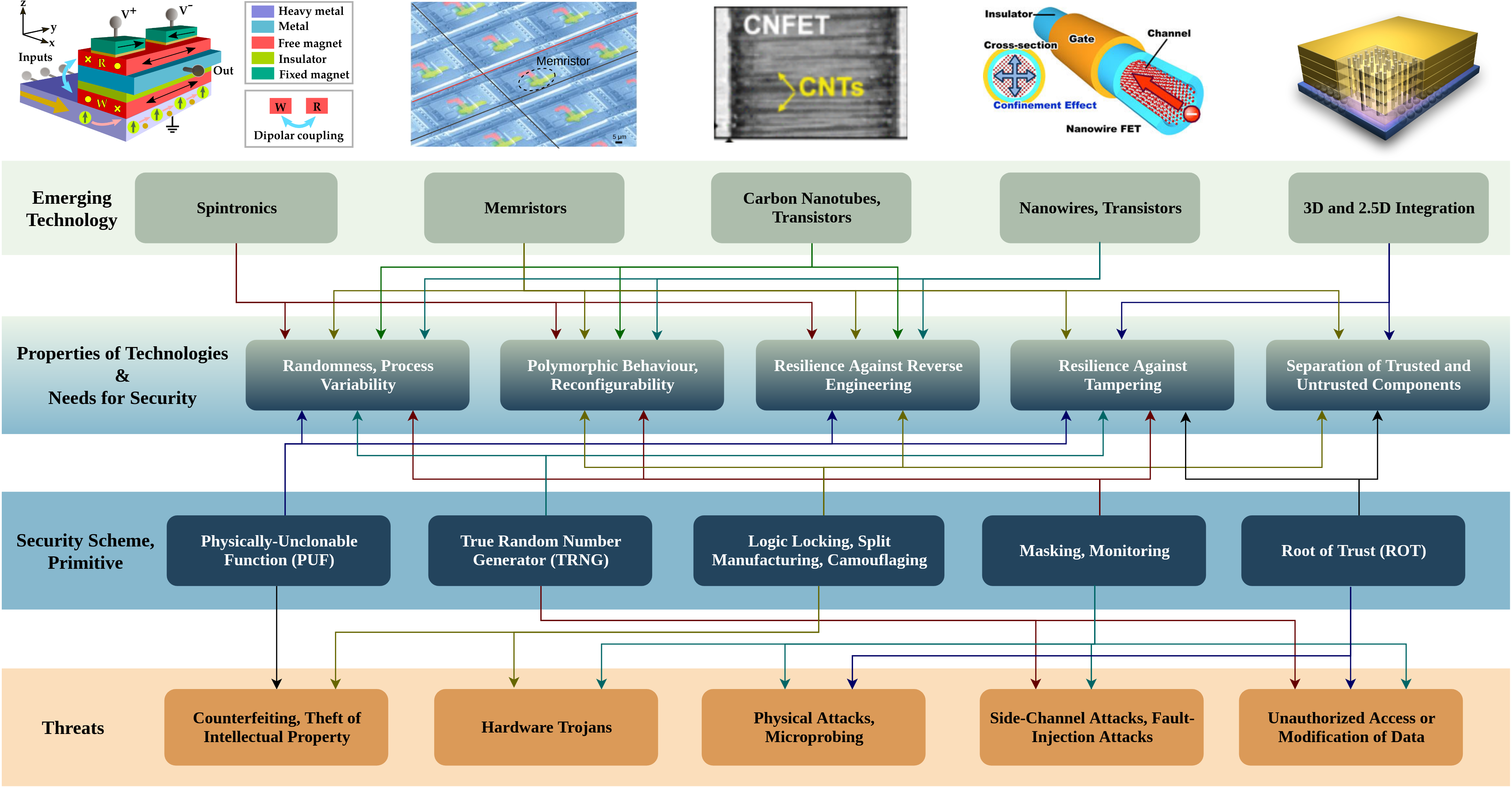
Various emerging technologies offer the potential to advance the notion of hardware security. In Fig. 1, I outline the selected emerging technologies covered in this paper, their properties relevant and beneficial for hardware security, the security schemes which are supported accordingly, and the security threats countered by such schemes. While this illustration is certainly not an overarching one, it does consider all the aspects introduced in this paper.
4.1. Emerging Devices
The reviewed emerging devices have some interesting properties in common, which are more difficult to achieve in traditional CMOS technology. More specifically, spintronics, memristors, CNTFETs, and NWFETs can all be tailored to comprise significant variability/randomness, reconfigurability or polymorphic behavior, resilience against reverse engineering, and possibly also for separation of trusted and untrusted parts (the latter by means of split manufacturing). Therefore, these devices can serve well for PUFs, TRNGs, IP protection schemes, and to mask side-channel leakage. Moreover, memristors may also offer resilience against tampering, by means of destructive data management (jiang18, ).
It should be understood that the prospects for actual implementation of such security schemes based on emerging devices depends on various aspects, ranging from circuit design and security analysis in general, down to manufacturing capabilities and device maturity, among others. Still, there is a wide range of prior art developing and promoting such schemes, of which some are reviewed next. Note that other papers have reviewed emerging devices in the context of hardware security as well, e.g., see (rajendran15_nano, ; ghosh16, ; rahman17, ).
4.1.1. Spintronics
Various studies proposed polymorphic behavior and/or reconfigurability for IP protection. For example, Alasad et al. (alasad2017leveraging, ) use all-spin logic for camouflaging. However, the layouts for some of their proposed device primitives are unique; they can be readily distinguished during imaging-based reverse engineering. Besides, their primitives suffer from relatively high energy consumption, with around 350 W consumed for ns-range delays. In (winograd2016hybrid, ; yang18, ), the authors introduced spintronics-based reconfigurable lookup tables (LUTs) for design obfuscation. However, these approaches can fall short regarding their resilience against SAT attacks (patnaik19_GSHE_TCAD, ). Also note that such approaches are conceptionally similar to design obfuscation leveraging traditional field-programmable gate arrays (FPGAs). In (parveen17, ) and (patnaik18_GSHE_DATE, ; patnaik19_GSHE_TCAD, ), polymorphic and obfuscated logic has been studied, based on domain-wall motion devices and on giant spin-Hall effect (GSHE) devices, respectively. One important benefit of the latter studies over the former is that they support all 16 possible functions per device; this renders these devices superior in terms of SAT resilience (patnaik18_GSHE_DATE, ; patnaik19_GSHE_TCAD, ).
In (rangarajan20_MESO_TETC, ), the notion of “dynamic camouflaging” based on polymorphic magnetoelectric spin-orbit (MESO) devices has been introduced. Unlike regular camouflaging, this notion can also protect against adversaries in the foundries and test facilities, as the true functionality is configured only later on within the polymorphic fabric. Thus, this notion is also conceptionally similar to logic locking; however, unlike with locking, no additional devices or gates are required to realize this kind of security.
It has been noted that spintronics can offer some resilience against side-channel attacks (patnaik19_GSHE_TCAD, ; rangarajan20_MESO_TETC, ; roohi19, ). For example, the magnetoelectric switching of these devices does not emit photons; related attacks as in (tajik17_CCS, ) can be ruled out to begin with. With spintronics used for logic, fault-injection and side-channel attacks based on magnetic fields or temperature curves may be more difficult to achieve (patnaik19_GSHE_TCAD, ; rangarajan20_MESO_TETC, ), unlike with spintronics used for memories (ghosh16, ). Moreover, in (roohi19, ) the authors used spintronics to build up polymorphic circuitry and different circuit templates for the same functionality, which are randomly switched between at runtime, in order to mask the power side-channel.
In (iyengar15S, ; ghosh16, ), the authors advocate the process variations for nanowire manufacturing in domain-wall memories for PUFs. In (rangarajan17_TRNG, ), the authors leverage the inherently stochastic spin switching mechanism in nanomagnets for TRNGs. Through device-level simulations, the authors demonstrate that their TRNG device works across large temperature ranges, is immune to process variations, and can be implemented with significantly smaller layout costs than CMOS TRNGs. In (rangarajan20_SMART_ACC, ), the authors propose an antiferromagnets-based secure memory scheme, which offers protection against tampering, side-channel, and read-out attacks, and also promises orders of lower energy-per-bit than STT-RAM or PCMs.
Most studies focus on circuit design and security analysis, but few on technology aspects. While spintronics are making fast progress toward application, it seems important to consider technology exploration also within the concerned security studies.
4.1.2. Memristors
The potential of using memristors for hardware-security schemes has been recognized already some years ago, e.g., for PUFs leveraging the process variations and the stochastic operation of memristors in 2013 (rose13, ). More recently, another PUF concept has been proposed (nili18, ), which leverages the non-linear I-V characteristics of memristors (“pinched hysteresis”) and applies analogue tuning of the memristor conductance, to increase the performance and practicality of such PUFs and to reduce the complexity of the peripheral circuitry. The authors of (nili18, ) provided an experimental demonstration and measurement results for their PUF concept.
In (jiang18, ), a memristive crossbar array is at the heart for secure management of secret keys. The authors propose to combine unique fingerprints of memristor devices with storage of key values within those devices. They construct control circuitry such that upon extraction of the fingerprints (for verification of authenticity of the chip), the key is destroyed. Therefore, the secret key remains “alive” on the chip to enable its functionality (following the notion of logic locking) until any read-out is conducted. The authors of (jiang18, ) provide an experimental demonstration and measurement results for their concept. Such a concept is an important step for the practicality of logic locking, which requires tamper-proof memories for its security promises against malicious end-users in the field.
In (rezaei19, ), the authors propose polymorphic circuitry for obfuscation also in the context of memristors. That is possible because, in principle, the functionality of memristor devices within such obfuscated logic can be reconfigured. While the authors provide a first study at the circuit and layout level—albeit without details on the technology exploration and library characterization—they do not provide any experimental demonstration. Moreover, other studies caution about delay and power consumption for memristor-based logic unless circuit structures are optimized (7811204, ), which seems to conflict with obfuscation principles.
4.1.3. CNTs and CNTFETs
In (liu18, ), the authors propose PUFs which leverage the manufacturing variability of CNTs along with the notion of Lorenz chaotic systems. The latter serves to enhance the decorrelation of inputs and outputs for such PUFs and, thus, renders them more resilient against machine-learning attacks.
In (suresh16, ), the authors conduct a simulations-based study on CNTFETS concerning Trojan detection, power side-channel leakage, and camouflaging, and they find that CNTFETs are more promising in all aspects when compared to the traditional CMOS technology.
In (rahman17, ), the authors review the use of CNTS for PUFs, TRNGs, and also propose the technology to be used for novel sensors detecting microprobing or other invasive attacks.
4.1.4. Nanowires and NWFETs
In (bi16_JETC, ), the authors propose silicon NWFETs for camouflaging. More specifically, they leverage the controllable ambipolarity in NWFETs to build up a camouflaging primitive comprising the NAND, NOR, XOR, and XNOR functionalities. The authors also build up a polymorphic NAND/NOR gate, and they present circuit-simulation results. In (patnaik19_GSHE_TCAD, ), however, it was shown that such primitives are prone to SAT attacks.
In (rai20_RFET_TETC, ), the authors first explore how transistor-level reconfigurability can be leveraged for logic locking and split manufacturing in the context of silicon NWFETS models. Second, they study how the very reconfigurability can be exploited to induce either short-circuit currents or open-circuit configurations, essentially annihilating the reliability and functional properties of the chip; the authors argue that this critical property of reconfigurable NWFETs could be either maliciously exploited as reliability-centric Trojan or intentionally leveraged as “kill switch.”
In (cui14_plasmonics, ; park16_plasmonics, ) the use of nanowires with plasmonics interaction upon optical inspection is proposed and experimentally demonstrated. This idea serves for labelling and authentication of chips (or other goods, for that matter). Loosely related, because without the need for nanowires, the authors in (knechtel19_peo-PUF_JLT, ) proposed the concept of plasmonics-enhanced optical PUFs and provide physical-simulation results and a security analysis.
4.2. 3D and 2.5D Integration
The main benefits provided by 3D and 2.5D integration to advance hardware security are (i) the physical separation of components, be it across interconnects, active devices, or both, and (ii) the physical enclosure of components, to shield them from adversarial activities in the field. In Table 1, I summarize selected works; I discuss these and others in some detail next. Note that other papers have reviewed the benefits and fallacies for hardware security arising by 3D and 2.5D integration as well, e.g., see (knechtel19_3D_IOLTS, ; xie16, ; dofe17, ).
| Reference | Style | Scope; Means | Trusted Part |
|---|---|---|---|
| (valamehr13, ) | TSV | Runtime monitoring; | Whole 3D IC |
| split manufacturing (SM) | |||
| (xie17, ) | 2.5D | IP protection; SM | Interposer |
| (imeson13, ) | 2.5D | Trojan prevention; SM | Interposer |
| (gu18, ) | F2F | IP protection; SM, camouflaging | Parts of 3D IC |
| (yan17_camo, ) | M3D | IP protection; camouflaging | Whole 3D IC |
| (patnaik19_3D_TETC, ) | F2F | IP protection, Trojan prevention; | Only BEOL |
| SM, camouflaging | |||
| (cioranesco14, ) | TSV | Probing protection; enclosure | Whole 3D IC |
| (knechtel17_TSC_DAC, ; bao17, ) | TSV | Side-channel mitigation; enclosure | Whole 3D IC |
| (nabeel20_ROT_TC, ) | 2.5D | Runtime monitoring; separation | Interposer |
4.2.1. Confidentiality and Integrity of Hardware: Logic Locking
To the best of our knowledge, 3D and 2.5D integration has not been explored yet for logic locking. In the loosely related work (sengupta19_LL_SM_DATE, ), the authors leverage locking principles to advance the notion of split manufacturing. More specifically, they lock the FEOL and delegate the unlocking to a separate, trusted BEOL facility. The authors note that their scheme can also be unlocked at the package or board level, which might well suggest an implementation as 2.5D IC.
4.2.2. Confidentiality and Integrity of Hardware: Camouflaging
The authors of (yan17_camo, ) were the first to propose camouflaging dedicatedly for 3D integration, more specifically for M3D ICs. The authors developed and characterized custom M3D camouflaged libraries, and they evaluated their scheme at the gate level and at chip scale.
The camouflaging is realized by dummy contacts, which has been proposed previously for camouflaging in classical 2D ICs. Thus, while conceptionally not new, the work in (yan17_camo, ) leverages the benefits provided by M3D ICs in an effort to advance the scalability of camouflaging. That is noteworthy because prior art for camouflaging may incur considerable layout cost. For example, the NAND-NOR-XOR primitive of (rajendran13_camouflage, ) would incur 5.5 power, 1.6 delay, and 4 area cost compared to a regular NAND gate. In practice, such cost allow for only few gates being camouflaged; in turn, limited camouflaging scales renders such schemes prone to SAT attacks (yu17, ; shamsi17, ). In contrast, the work in (yan17_camo, ) report on average only 25% power cost, 15% delay cost, and 43% area savings compared to regular 2D gates.
4.2.3. Confidentiality and Integrity of Hardware: Split Manufacturing
To advance split manufacturing via 3D and 2.5D integration seems both straightforward and promising. That is because 3D and 2.5D integration allows to split a design into multiple chips, which can maintain their FEOL and BEOL layers independently as is, whereas the overall 2.5D/3D stack can comprise further parts of the system-level interconnects. Moreover, concerns regarding the practicability of classical split manufacturing—which are still prevalent, despite proof-of-concept studies like (vaidyanathan14_2, ; mccants16, )—can be elevated due to this very fact that individual chip would not have to be split manufactured, but only the overall system.
The idea of such “3D split manufacturing” was outlined in 2008, by Tezzaron Semiconductor (tezzaron08, ). Various studies are hinting at 3D split manufacturing as well, but most have some limitations. For example, the study (dofe17, ) remains only on the conceptional level, while the studies (xie17, ; imeson13, ) utilize 2.5D integration with “only” wires being hidden from untrusted facilities. The latter is in principal equivalent to traditional split manufacturing but seems more practical; still, the studies (xie17, ; imeson13, ) report on considerable layout cost. Later on, (devale17, ; gu18, ; patnaik18_3D_ICCAD, ; patnaik19_3D_TETC, ) promoted “native 3D split manufacturing,” i.e., with logic being split across trusted and untrusted facilities.
One important finding of those later studies (devale17, ; gu18, ; patnaik18_3D_ICCAD, ; patnaik19_3D_TETC, ) is that the 3D partitioning as well as the vertical interconnect fabric both play an important role and define a cost-security trade-off as follows: the more the design is split up across multiple chips, the higher the layout cost, due to the need for more vertical interconnect links and related circuitry, but the more flexible and easier it becomes to “dissolve” the IP across the 3D stack.
Note that (gu18, ; patnaik18_3D_ICCAD, ; patnaik19_3D_TETC, ) proposed 3D split manufacturing in conjunction with camouflaging. While the study (gu18, ) applies regular, FEOL-centric camouflaging, the studies (patnaik18_3D_ICCAD, ; patnaik19_3D_TETC, ) argue that another camouflaging approach is more appropriate for 3D split manufacturing, namely the obfuscation of the vertical interconnects. Other works also suggest camouflaging at the system level. For example, (dofe16, ) proposed to obfuscate the vertical interconnect fabric of 3D ICs by rerouting within dedicated network-on-chip (NoC) chips “sandwiched” between the regular chips. This idea is conceptionally similar to the notion of randomized routing in (patnaik18_3D_ICCAD, ; patnaik19_3D_TETC, ), but more flexible, yet also more costly—it seems only warranted in case 3D NoCs are to be employed in any case.
4.2.4. Confidentiality and Integrity of Hardware: Trojan Defense
In (patnaik19_3D_TETC, ), the authors leveraged the benefits provided by 3D split manufacturing to advance the formally-secure but high-cost scheme of (imeson13, ) to mitigate Trojan insertion at manufacturing time.
Besides, 3D and 2.5D ICs seem rather more vulnerable than 2D ICs to Trojan insertion during design and manufacturing time. For example, the study in (mossa17, ) considered the negative bias temperature instability (NBTI) effect as stealthy Trojan trigger, motivated by the fact that thermal management is a well-known challenge for 3D ICs. In a more general manner, I caution that the broader landscape of suppliers and actors involved with 3D and 2.5D integration can open up new opportunities for attackers to embed Trojans. Such a concern has also been voiced recently in (bunnie_36c3, ), along with the wide-spread adoption of wafer-level chip-scale packaging (WLCSP). The hypothesized attack here is that some malicious integration facility could place a thin Trojan chip between the target chip and the package microbumps, while that Trojan chip would contain TSVs to both pass-through and tap into those external connections, gaining access to all these signals at will. To mitigate detection by visual or X-ray inspection, it was argued that aligning those TSVs with the microbump locations might suffice.
Trojan detection at runtime, however, can benefit from 3D and 2.5D integration. That is because related security features can be implemented separately using a trusted fabrication process and integrated/stacked later on with the commodity chip(s) to be monitored (wahby16, ; nabeel20_ROT_TC, ); see also the discussion on data security below.
4.2.5. Confidentiality and Integrity of Hardware: PUFs
The integration of multiple chips into 3D/2.5D stacks seems beneficial for the notion of PUFs, as the individual chips are subject to independent process variations. Thus, one can build up PUFs using multiple, independent sources of entropy. In (wang14_SuperPUF, ; wang15_TSV-PUF, ), two such schemes have been proposed, which further leverage the process variations of TSVs. While promising in principle, these studies did not consider state-of-the-art machine learning attacks like (chang17_PUF, ; ruehrmair13, ; liu17, ; ganji17_thesis, ); their actual resilience remains yet to be demonstrated.
4.2.6. Data Security at Runtime: Unauthorized Access or Modification of Data
3D and 2.5D integration enables physical separation of components and, thus, allows for trustworthy realization of security features like runtime monitors (mysore06, ; valamehr13, ; nabeel20_ROT_TC, ) or verifiers (wahby16, ).
Still, I caution that the physical implementation of such schemes may become a vulnerability by itself. In (valamehr13, ), for example, the authors propose introspective interfaces which, however, require additional logic within the commodity chip to be monitored. It is easy to see that these interfaces would fail once they are modified by some malicious actor(s) involved with the design or manufacturing of that commodity chip. Thus, an undesirable dependency arises, possibly thwarting the scheme altogether. Note that the authors themselves acknowledge this limitation in (valamehr13, ).
In (nabeel20_ROT_TC, ), a 2.5D root of trust has been proposed, which integrates untrusted commodity chips/chiplets onto an active interposer which contains security features and further forms the backbone for system-level communication between the chips/ciplets. Thus, a clear physical separation into commodity and security components exists, avoiding any security-undermining dependencies.
4.2.7. Data Security at Runtime: Side-Channel and Fault-Injection Attacks
In general, side-channel attacks seem to become more difficult for 3D and 2.5D ICs, considering the higher density of active devices and the more complex circuit structures and architectures, which can result into more noisy side-channels. For example, the authors of (dofe18_PDN, ) studied power side-channel attacks on 3D ICs, and they observed that the power noise profiles from the different chips within the 3D IC are superposed. They also propose a randomized cross-linking scheme of voltage supplies for cryptographic modules, to render attacks on such modules more difficult.
Some prior art also studied side-channel attacks targeted explicitly for 3D ICs. For example, (gu16_ICCD, ) and (knechtel17_TSC_DAC, ) demonstrate that thermal side-channel attacks on 3D ICs can be mitigated at runtime and at design time, respectively. However, the approach in (gu16_ICCD, ) seems less practical; to mitigate information leakage through thermal patterns, it leverages dynamic generation of additional dummy activities, which exacerbates the challenge of thermal management for 3D ICs even further. In contrast, the authors of (knechtel17_TSC_DAC, ) model the impact of TSVs and module placement on heat distribution as well as thermal leakage during floorplanning, thereby enabling leakage mitigation along with reduction of peak temperatures.
Besides, some studies leverage 3D and 2.5D integration to advocate for security schemes otherwise considered too costly. For example, the study in (bao15, ) leverages randomized eviction and heterogeneous latencies for a cache architecture. The authors demonstrate that such techniques incur high performance overheads in 2D ICs but can be realized even with gains in 3D ICs.
As with side-channel attacks, fault-injection attacks may become more difficult, due to the physical encapsulation of 3D/2.5D ICs. Still, in (rodriguez19, ) it was shown recently that a lateral re-arrangement of the laser setup can suffice to enable such fault-injection attacks also for backside-protected 2D ICs and possibly also for 2.5D and 3D ICs. However, with a dedicated physical design of 3D ICs, e.g., placing TSVs densely at the chip boundaries, forming a “vertical shield” structure (knechtel19_3D_IOLTS, ), along with regular shields in the BEOL and backside protection, even such attacks might remain difficult.
4.2.8. Data Security at Runtime: Physical Read-Out and Probing Attacks
Similar to fault-injection attacks, the notion of physical enclosures enabled by 3D/2.5D integration may hinder read-out and probing attacks. In (knechtel19_3D_IOLTS, ), the authors argued for “all around shields” enabled by 3D ICs. Similar protection against probing has been discussed before in (briais12, ; cioranesco14, ). While powerful in principle, such schemes are yet to be demonstrated in practice.
5. Challenges for Hardware Security Using Emerging Technologies
As with any security scheme, also those relying on emerging technologies face some challenges. I have outlined specific limitations and challenges for selected prior art already in the discussion above, but here I seek to take a broader view.
Possibly the most important and complex challenges arise from the fact that security schemes in general and those based on emerging technologies in particular rely on proper technology exploration, device characterization and modeling, circuit architectures, design strategies, etc. While security schemes tailored for CMOS technology can leverage well-defined and well-characterized technology libraries, state-of-the-art design tools,333Even in the context of classical CMOS technology, there are still a plethora of challenges to be addressed to make design tools more security-aware (knechtel20_Sec_EDA_DATE, ). etc., this is not so straightforward for most emerging technologies, as their characterization and design support is still progressing. However, the resulting challenges may—and should—be rather considered as chances, namely to incorporate security as best as possible right from the beginning, and not only as an afterthought, as we often see for security schemes using CMOS technology.
To do so, I propose that the following steps, among others and not necessarily in that particular order, are to be considered:
-
(1)
Establish closer interaction between the communities working on hardware security, physical design, and emerging technologies. I argue that a collaborative exchange between our communities is essential for any advancement.
-
(2)
(Re-)definition of security metrics and joint “translation” of those metrics. Only then can the emerging-technology communities consider hardware security in a proper, quantifiable manner during technology exploration and device design. For example, while the correlation of switching activities and power consumption (for estimation of power side-channel leakage) seems rather easy to model also for emerging technologies, the commonly promoted criteria for PUFs, like uniqueness or unpredictability, are highly device-specific and require “translation” for effective modeling.
-
(3)
Joint reconsideration of threat models. With the progression of emerging technologies, it can be expected that further fallacies, possibly yet unexplored, come into play. For example, advanced tools for failure analysis of emerging technologies can be “misused” for physical attacks in the field. For security schemes based on CMOS technology, we have seen this with the proliferation and wider availability of, e.g., electron microscopy (sugawara14, ) and electro-optical probing (tajik17_CCS, ).
-
(4)
Technology exploration, prototyping, and joint evaluation of securities schemes based on emerging technologies. That is also because process variations are expected to be more pronounced for most emerging technologies. For PUFs, e.g., stronger variations would serve well for uniqueness/entropy, but hinder reproducibility. Only once such empirical insights are available it would seem possible to devise, e.g., error correction schemes to improve the reproducibility.
-
(5)
Since most emerging technologies are being promoted for CMOS integration, it becomes important to determine the “weakest link(s) in the chain” for such hybrid implementations of security schemes. These efforts should range from device to circuit to system level, and should also revise related design strategies as needed. Somewhat related, note that the composition of security schemes remains a challenge even for CMOS-only ICs; the physical-design community should become more involved here as well (knechtel20_Sec_EDA_DATE, ).
6. Conclusion
In this paper, I have reviewed the fundamentals of hardware security in general and discussed selected prior art. I have further reviewed selected emerging technologies, namely (i) spintronics, (ii) memristors, (iii) carbon nanotubes and related transistors, (iv) nanowires and related transistors, and (v) 3D and 2.5D integration. I have discussed how these technologies are promising to advance various aspects of hardware security, and I have also reviewed related early studies and some of their limitations. Note that I made an effort to include hyperlinks for each and every reference, which should serve well for further literature study of any interested reader.
Many of the security schemes based on emerging technologies still require more collaborative efforts and practical validation—which is not to be taken as pessimistic statement, rather as call to our communities for joint action.
References
- (1) B. Krebs. (2019) First american financial corp. leaked hundreds of millions of title insurance records. https://krebsonsecurity.com/2019/05/first-american-financial-corp-leaked-hundreds-of-millions-of-title-insurance-records/
- (2) P. Maene et al., “Hardware-based trusted computing architectures for isolation and attestation,” Trans. Comp., vol. 67, no. 3, pp. 361–374, 2018. https://doi.org/10.1109/TC.2017.2647955
- (3) M. Nabeel et al., “2.5D root of trust: Secure system-level integration of untrusted chiplets,” Trans. Comp., vol. 69, pp. 1611–1625, 2020. https://doi.org/10.1109/TC.2020.3020777
- (4) H. Jiang et al., “A provable key destruction scheme based on memristive crossbar arrays,” Nature Electronics, vol. 1, no. 10, pp. 548–554, 2018. https://doi.org/10.1038/s41928-018-0146-5
- (5) E. Brier, C. Clavier, and F. Olivier, “Correlation power analysis with a leakage model,” in Proc. Cryptogr. Hardw. Embed. Sys., 2004. https://doi.org/10.1007/978-3-540-28632-5_2
- (6) P. Bayon et al., “Fault model of electromagnetic attacks targeting ring oscillator-based true random number generators,” J. Cryptogr. Eng., vol. 6, no. 1, pp. 61–74, 2016. https://doi.org/10.1007/s13389-015-0113-2
- (7) P. Qiu, D. Wang, Y. Lyu, and G. Qu, “VoltJockey: Breaching TrustZone by software-controlled voltage manipulation over multi-core frequencies,” in Proc. Comp. Comm. Sec., 2019, pp. 195–209. https://doi.org/10.1145/3319535.3354201
- (8) Y. Zhou and D. Feng, “Side-channel attacks: Ten years after its publication and the impacts on cryptographic module security testing,” in IACR Crypt. ePrint Arch., no. 388, 2005. http://eprint.iacr.org/2005/388
- (9) D. A. Osvik, A. Shamir, and E. Tromer, “Cache attacks and countermeasures: the case of AES,” in IACR Crypt. ePrint Arch., 2005. https://eprint.iacr.org/2005/271
- (10) M. Schwarz et al., “ZombieLoad: Cross-privilege-boundary data sampling,” Comp. Research Rep., 2019. https://arxiv.org/abs/1905.05726
- (11) H. Groß, S. Mangard, and T. Korak, “Domain-oriented masking: Compact masked hardware implementations with arbitrary protection order,” in Proc. Comp. Comm. Sec., 2016. https://doi.org/10.1145/2996366.2996426
- (12) D. Bellizia et al., “Secure double rate registers as an RTL countermeasure against power analysis attacks,” Trans. VLSI Syst., vol. 26, no. 7, pp. 1368–1376, 2018. https://doi.org/10.1109/TVLSI.2018.2816914
- (13) B. Selmke, J. Heyszl, and G. Sigl, “Attack on a DFA protected AES by simultaneous laser fault injections,” in Proc. Worksh. Fault Diag. Tol. Cryptogr., 2016, pp. 36–46. https://doi.org/10.1109/FDTC.2016.16
- (14) A. Dehbaoui, J. Dutertre, B. Robisson, and A. Tria, “Electromagnetic transient faults injection on a hardware and a software implementations of AES,” in Proc. Worksh. Fault Diag. Tol. Cryptogr., 2012, pp. 7–15. https://doi.org/10.1109/FDTC.2012.15
- (15) V. van der Veen et al., “Drammer: Deterministic rowhammer attacks on mobile platforms,” in Proc. Comp. Comm. Sec., 2016, pp. 1675–1689. https://doi.org/10.1145/2976749.2978406
- (16) G. D. Natale, E. I. Vatajelu, K. S. Kannan, and L. Anghel, “Hidden-delay-fault sensor for test, reliability and security,” in Proc. Des. Autom. Test Europe, 2019, pp. 316–319. https://doi.org/10.23919/DATE.2019.8714891
- (17) B. Karp, M. Gay, O. Keren, and I. Polian, “Security-oriented code-based architectures for mitigating fault attacks,” in Proc. DCIS, 2018, pp. 1–6. https://doi.org/10.1109/DCIS.2018.8681476
- (18) J. Dutertre et al., “Laser fault injection at the CMOS 28 nm technology node: an analysis of the fault model,” in Proc. Worksh. Fault Diag. Tol. Cryptogr., 2018. https://doi.org/10.1109/FDTC.2018.00009
- (19) B. Karp, M. Gay, O. Keren, and I. Polian, “Detection and correction of malicious and natural faults in cryptographic modules,” in Proc. PROOFS@CHES, 2018, pp. 68–82. https://easychair.org/publications/download/zMjh
- (20) E. L. Principe et al., “Plasma FIB deprocessing of integrated circuits from the backside,” Elec. Dev. Fail. Analysis, vol. 19, no. 4, pp. 36–44, 2017. https://www.researchgate.net/profile/Robert_Chivas/publication/322264562_Plasma_FIB_deprocessing_of_integrated_circuits_from_the_backside/links/5a54f88e45851547b1bd55f2/Plasma-FIB-deprocessing-of-integrated-circuits-from-the-backside.pdf
- (21) H. Wang, Q. Shi, D. Forte, and M. M. Tehranipoor, “Probing attacks on integrated circuits: Challenges and research opportunities,” Des. Test, vol. 34, no. 5, pp. 63–71, 2017. https://doi.org/10.1109/MDAT.2017.2729398
- (22) C. Helfmeier et al., “Breaking and entering through the silicon,” in Proc. Comp. Comm. Sec., 2013, pp. 733–744. https://doi.org/10.1145/2508859.2516717
- (23) S. Tajik, H. Lohrke, J.-P. Seifert, and C. Boit, “On the power of optical contactless probing: Attacking bitstream encryption of FPGAs,” in Proc. Comp. Comm. Sec., 2017, pp. 1661–1674. https://doi.org/10.1145/3133956.3134039
- (24) T. Krachenfels et al., “Real-world snapshots vs. theory: Questioning the t-probing security model,” 2020. https://arxiv.org/abs/2009.04263
- (25) F. Courbon, S. Skorobogatov, and C. Woods, “Direct charge measurement in floating gate transistors of flash EEPROM using scanning electron microscopy,” in Proc. Int. Symp. Test. Failure Analys., 2016, pp. 1–9. https://pdfs.semanticscholar.org/992a/20c0a8bb71642fc44fa65f053b3524113b99.pdf
- (26) Y. Lee, H. Lim, Y. Lee, and S. Kang, “Robust secure shield architecture for detection and protection against invasive attacks,” Trans. Comp.-Aided Des. Integ. Circ. Sys., 2019. https://doi.org/10.1109/TCAD.2019.2944580
- (27) K. Yi, M. Park, and S. Kim, “Practical silicon-surface-protection method using metal layer,” J. Semicond. Tech. Sci., vol. 16, no. 4, pp. 470–480, 2016. https://doi.org/10.5573/JSTS.2016.16.4.470
- (28) H. Shen, N. Asadizanjani, M. Tehranipoor, and D. Forte, “Nanopyramid: An optical scrambler against backside probing attacks,” in Proc. Int. Symp. Test. Failure Analys., 2018. https://pdfs.semanticscholar.org/453a/ce0749c374d59c4193cc26d06ac38e22c500.pdf
- (29) M. Weiner, S. Manich, R. Rodríguez-Montañés, and G. Sigl, “The low area probing detector as a countermeasure against invasive attacks,” Trans. VLSI Syst., vol. 26, no. 2, pp. 392–403, 2018. https://doi.org/10.1109/TVLSI.2017.2762630
- (30) Y. Ishai, A. Sahai, and D. Wagner, “Private circuits: Securing hardware against probing attacks,” in Advances in Cryptology, 2003, pp. 463–481. https://doi.org/10.1007/978-3-540-45146-4_27
- (31) M. Rostami, F. Koushanfar, and R. Karri, “A primer on hardware security: Models, methods, and metrics,” Proc. IEEE, vol. 102, no. 8, pp. 1283–1295, 2014. https://doi.org/10.1109/JPROC.2014.2335155
- (32) J. Knechtel, S. Patnaik, and O. Sinanoglu, “Protect your chip design intellectual property: An overview,” in Proc. Conf. Omni-Layer Intell. Sys., 2019, pp. 211–216. https://doi.org/10.1145/3312614.3312657
- (33) M. Yasin, J. J. Rajendran, and O. Sinanoglu, Trustworthy Hardware Design: Combinational Logic Locking Techniques. Springer, 2020. https://doi.org/10.1007/978-3-030-15334-2
- (34) M. Yasin, S. M. Saeed, J. Rajendran, and O. Sinanoglu, “Activation of logic encrypted chips: Pre-test or post-test?” in Proc. Des. Autom. Test Europe, 2016, pp. 139–144. https://ieeexplore.ieee.org/abstract/document/7459294
- (35) J. A. Roy, F. Koushanfar, and I. L. Markov, “Ending piracy of integrated circuits,” Computer, vol. 43, no. 10, pp. 30–38, 2010. https://doi.org/10.1109/MC.2010.284
- (36) M. Yasin, J. J. Rajendran, O. Sinanoglu, and R. Karri, “On improving the security of logic locking,” Trans. Comp.-Aided Des. Integ. Circ. Sys., vol. 35, no. 9, pp. 1411–1424, 2016. https://doi.org/10.1109/TCAD.2015.2511144
- (37) P. Subramanyan, S. Ray, and S. Malik, “Evaluating the security of logic encryption algorithms,” in Proc. Int. Symp. Hardw.-Orient. Sec. Trust, 2015, pp. 137–143. https://doi.org/10.1109/HST.2015.7140252
- (38) Y. Xie and A. Srivastava, “Mitigating SAT attack on logic locking,” in Proc. Cryptogr. Hardw. Embed. Sys., 2016, pp. 127–146. https://doi.org/10.1007/978-3-662-53140-2_7
- (39) M. Yasin et al., “Provably-secure logic locking: From theory to practice,” in Proc. Comp. Comm. Sec., 2017, pp. 1601–1618. https://doi.org/10.1145/3133956.3133985
- (40) Y. Shen and H. Zhou, “Double DIP: Re-evaluating security of logic encryption algorithms,” in Proc. Great Lakes Symp. VLSI, 2017, pp. 179–184. https://doi.org/10.1145/3060403.3060469
- (41) K. Shamsi et al., “AppSAT: Approximately deobfuscating integrated circuits,” in Proc. Int. Symp. Hardw.-Orient. Sec. Trust, 2017, pp. 95–100. https://doi.org/10.1109/HST.2017.7951805
- (42) L. Alrahis et al., “UNSAIL: Thwarting oracle-less machine learning attacks on logic locking,” Trans. Inf. Forens. Sec., vol. 16, pp. 2508–2523, 2021. https://doi.org/10.1109/TIFS.2021.3057576
- (43) L. Li and A. Orailoglu, “Piercing logic locking keys through redundancy identification,” in Proc. Des. Autom. Test Europe, 2019. https://doi.org/10.23919/DATE.2019.8714955
- (44) J. Rajendran, M. Sam, O. Sinanoglu, and R. Karri, “Security analysis of integrated circuit camouflaging,” in Proc. Comp. Comm. Sec., 2013, pp. 709–720. https://doi.org/10.1145/2508859.2516656
- (45) B. Erbagci, C. Erbagci, N. E. C. Akkaya, and K. Mai, “A secure camouflaged threshold voltage defined logic family,” in Proc. Int. Symp. Hardw.-Orient. Sec. Trust, 2016, pp. 229–235. https://doi.org/10.1109/HST.2016.7495587
- (46) M. Li et al., “Provably secure camouflaging strategy for IC protection,” in Proc. Int. Conf. Comp.-Aided Des., 2016, pp. 28:1–28:8. https://doi.org/10.1145/2966986.2967065
- (47) S. Patnaik, M. Ashraf, O. Sinanoglu, and J. Knechtel, “Obfuscating the interconnects: Low-cost and resilient full-chip layout camouflaging,” Trans. Comp.-Aided Des. Integ. Circ. Sys., vol. 39, pp. 4466–4481, 2020. https://doi.org/10.1109/TCAD.2020.2981034
- (48) (2019) Circuit camouflage technology. Rambus Inc. https://www.rambus.com/security/cryptofirewall-cores/circuit-camouflage-technology/
- (49) Y. Lao and K. K. Parhi, “Obfuscating DSP circuits via high-level transformations,” Trans. VLSI Syst., vol. 23, no. 5, pp. 819–830, 2015. https://doi.org/10.1109/TVLSI.2014.2323976
- (50) C. Yu et al., “Incremental SAT-based reverse engineering of camouflaged logic circuits,” Trans. Comp.-Aided Des. Integ. Circ. Sys., vol. 36, no. 10, pp. 1647–1659, 2017. https://doi.org/10.1109/TCAD.2017.2652220
- (51) A. Vijayakumar et al., “Physical design obfuscation of hardware: A comprehensive investigation of device- and logic-level techniques,” Trans. Inf. Forens. Sec., vol. 12, no. 1, pp. 64–77, 2017. https://doi.org/10.1109/TIFS.2016.2601067
- (52) J. Rajendran, O. Sinanoglu, and R. Karri, “Is split manufacturing secure?” in Proc. Des. Autom. Test Europe, 2013, pp. 1259–1264. https://doi.org/10.7873/DATE.2013.261
- (53) A. Sengupta et al., “Rethinking split manufacturing: An information-theoretic approach with secure layout techniques,” in Proc. Int. Conf. Comp.-Aided Des., 2017, pp. 329–336. https://doi.org/10.1109/ICCAD.2017.8203796
- (54) A. Sengupta, M. Nabeel, J. Knechtel, and O. Sinanoglu, “A new paradigm in split manufacturing: Lock the FEOL, unlock at the BEOL,” in Proc. Des. Autom. Test Europe, 2019, pp. 414–419. https://doi.org/10.23919/DATE.2019.8715281
- (55) S. Patnaik, J. Knechtel, M. Ashraf, and O. Sinanoglu, “Concerted wire lifting: Enabling secure and cost-effective split manufacturing,” in Proc. Asia South Pac. Des. Autom. Conf., 2018, pp. 251–258. https://doi.org/10.1109/ASPDAC.2018.8297314
- (56) S. Patnaik, M. Ashraf, J. Knechtel, and O. Sinanoglu, “Raise your game for split manufacturing: Restoring the true functionality through BEOL,” in Proc. Des. Autom. Conf., 2018, pp. 140:1–140:6. https://doi.org/10.1145/3195970.3196100
- (57) C. McCants. (2016) Trusted integrated chips (TIC) program. https://www.ndia.org/-/media/sites/ndia/meetings-and-events/divisions/systems-engineering/past-events/trusted-micro/2016-august/mccants-carl.ashx
- (58) K. Vaidyanathan et al., “Building trusted ICs using split fabrication,” in Proc. Int. Symp. Hardw.-Orient. Sec. Trust, 2014, pp. 1–6. https://doi.org/10.1109/HST.2014.6855559
- (59) Y. Wang, P. Chen, J. Hu, and J. J. Rajendran, “The cat and mouse in split manufacturing,” in Proc. Des. Autom. Conf., 2016, pp. 165:1–165:6. https://doi.org/10.1145/2897937.2898104
- (60) H. Li et al., “Attacking split manufacturing from a deep learning perspective,” in Proc. Des. Autom. Conf., 2019, pp. 135:1–135:6. https://doi.org/10.1145/3316781.3317780
- (61) H. Li et al., “Deep learning analysis for split manufactured layouts with routing perturbation,” Trans. Comp.-Aided Des. Integ. Circ. Sys., vol. Early Access, 2020. https://doi.org/10.1109/TCAD.2020.3037297
- (62) S. Bhunia and M. M. Tehranipoor, Eds., The Hardware Trojan War: Attacks, Myths, and Defenses. Springer, 2018. https://doi.org/10.1007/978-3-319-68511-3
- (63) K. Basu et al., “CAD-Base: An attack vector into the electronics supply chain,” Trans. Des. Autom. Elec. Sys., vol. 24, no. 4, pp. 38:1–38:30, 2019. https://doi.org/10.1145/3315574
- (64) P. Swierczynski et al., “Interdiction in practice–hardware trojan against a high-security USB flash drive,” J. Cryptogr. Eng., vol. 7, no. 3, pp. 199–211, 2017. https://doi.org/10.1007/s13389-016-0132-7
- (65) Y. Jin and Y. Makris, “Hardware trojan detection using path delay fingerprint,” in Proc. Int. Symp. Hardw.-Orient. Sec. Trust, 2008, pp. 51–57. https://doi.org/10.1109/HST.2008.4559049
- (66) E. Love, Y. Jin, and Y. Makris, “Proof-carrying hardware intellectual property: A pathway to trusted module acquisition,” Trans. Inf. Forens. Sec., vol. 7, no. 1, pp. 25–40, 2012. https://doi.org/10.1109/TIFS.2011.2160627
- (67) X. Guo et al., “QIF-Verilog: Quantitative information-flow based hardware description languages for pre-silicon security assessment,” in Proc. Int. Symp. Hardw.-Orient. Sec. Trust, 2019, pp. 91–100. https://doi.org/10.1109/HST.2019.8740840
- (68) T. Sugawara et al., “Reversing stealthy dopant-level circuits,” J. Cryptogr. Eng., vol. 5, no. 2, pp. 85–94, 2015. https://doi.org/10.1007/s13389-015-0102-5
- (69) N. Vashistha et al., “Trojan scanner: Detecting hardware trojans with rapid SEM imaging combined with image processing and machine learning,” in Proc. Int. Symp. Test. Failure Analys., 2018. https://pdfs.semanticscholar.org/7b7d/582034c19096c28c47bd1452e8becf287abc.pdf
- (70) A. Chandrasekharan, K. Schmitz, U. Kuhne, and R. Drechsler, “Ensuring safety and reliability of IP-based system design – a container approach,” in Proc. Int. Symp. Rapid System Prototyping, 2015, pp. 76–82. https://doi.org/10.1109/RSP.2015.7416550
- (71) K. Xiao, D. Forte, and M. Tehranipoor, “A novel built-in self-authentication technique to prevent inserting hardware trojans,” Trans. Comp.-Aided Des. Integ. Circ. Sys., vol. 33, no. 12, pp. 1778–1791, 2014. https://doi.org/10.1109/TCAD.2014.2356453
- (72) L. W. Kim and J. D. Villasenor, “A system-on-chip bus architecture for thwarting integrated circuit trojan horses,” Trans. VLSI Syst., vol. 19, no. 10, pp. 1921–1926, 2011. https://doi.org/10.1109/TVLSI.2010.2060375
- (73) S. Bhunia et al., “Protection against hardware trojan attacks: Towards a comprehensive solution,” Des. Test, vol. 30, no. 3, pp. 6–17, 2013. https://doi.org/10.1109/MDT.2012.2196252
- (74) A. Basak, S. Bhunia, T. Tkacik, and S. Ray, “Security assurance for system-on-chip designs with untrusted IPs,” Trans. Inf. Forens. Sec., vol. 12, no. 7, pp. 1515–1528, 2017. https://doi.org/10.1109/TIFS.2017.2658544
- (75) T. F. Wu et al., “TPAD: Hardware trojan prevention and detection for trusted integrated circuits,” Trans. Comp.-Aided Des. Integ. Circ. Sys., vol. 35, no. 4, pp. 521–534, 2016. https://doi.org/10.1109/TCAD.2015.2474373
- (76) R. S. Wahby, M. Howald, S. Garg, and M. Walfish, “Verifiable ASICs,” Proc. Symp. Sec. Priv., pp. 759–778, 2016. https://doi.org/10.1109/SP.2016.51
- (77) F. Imeson, A. Emtenan, S. Garg, and M. V. Tripunitara, “Securing computer hardware using 3D integrated circuit (IC) technology and split manufacturing for obfuscation,” in Proc. USENIX Sec. Symp., 2013, pp. 495–510. https://www.usenix.org/conference/usenixsecurity13/technical-sessions/presentation/imeson
- (78) C. Herder, M. D. Yu, F. Koushanfar, and S. Devadas, “Physical unclonable functions and applications: A tutorial,” Proc. IEEE, vol. 102, no. 8, pp. 1126–1141, 2014. https://doi.org/10.1109/JPROC.2014.2320516
- (79) R. Maes and I. Verbauwhede, Physically Unclonable Functions: A Study on the State of the Art and Future Research Directions. Springer, 2010, pp. 3–37. https://doi.org/10.1007/978-3-642-14452-3_1
- (80) C. H. Chang, Y. Zheng, and L. Zhang, “A retrospective and a look forward: Fifteen years of physical unclonable function advancement,” IEEE Circuits and Systems Magazine, vol. 17, no. 3, pp. 32–62, 2017. https://doi.org/10.1109/MCAS.2017.2713305
- (81) F. Ganji, “On the learnability of physically unclonable functions,” Ph.D. dissertation, TU Berlin, 2017. https://doi.org/10.14279/depositonce-6174
- (82) U. Rührmair et al., “PUF modeling attacks on simulated and silicon data,” Trans. Inf. Forens. Sec., vol. 8, no. 11, pp. 1876–1891, 2013. https://doi.org/10.1109/TIFS.2013.2279798
- (83) Y. Liu, Y. Xie, C. Bao, and A. Srivastava, “A combined optimization-theoretic and side-channel approach for attacking strong physical unclonable functions,” Trans. VLSI Syst., vol. 26, no. 1, pp. 73–81, 2018. https://doi.org/10.1109/TVLSI.2017.2759731
- (84) R. Pappu, B. Recht, J. Taylor, and N. Gershenfeld, “Physical one-way functions,” Science, vol. 297, no. 5589, pp. 2026–2030, 2002. https://doi.org/10.1126/science.1074376
- (85) U. Rührmair et al., “Optical PUFs reloaded,” in IACR Crypt. ePrint Arch., 2013. https://eprint.iacr.org/2013/215
- (86) P. Tuyls and B. Škorić, Strong Authentication with Physical Unclonable Functions. Springer, 2007, pp. 133–148. https://doi.org/10.1007/978-3-540-69861-6_10
- (87) B. C. Grubel et al., “Silicon photonic physical unclonable function,” Opt. Express, vol. 25, no. 11, pp. 12 710–12 721, 2017. https://doi.org/10.1364/OE.25.012710
- (88) J. Knechtel et al., “Toward physically unclonable functions from plasmonics-enhanced silicon disc resonators,” J. Lightwave Tech., vol. 37, pp. 3805–3814, 2019. https://doi.org/10.1109/JLT.2019.2920949
- (89) H. Amrouch et al., “Negative capacitance transistor to address the fundamental limitations in technology scaling: Processor performance,” IEEE Access, vol. 6, pp. 52 754–52 765, 2018. https://doi.org/10.1109/ACCESS.2018.2870916
- (90) J. Knechtel et al., “Power side-channel attacks in negative capacitance transistor,” Proc. Int. Symp. Microarch., vol. 40, pp. 74–84, 2020. https://doi.org/10.1109/MM.2020.3005883
- (91) D. Perez et al., “Multipurpose silicon photonics signal processor core,” Nature Communications, vol. 8, no. 1, p. 636, Sep. 2017. https://doi.org/10.1038/s41467-017-00714-1
- (92) J. S. Orcutt et al., “Open foundry platform for high-performance electronic-photonic integration,” Opt. Express, vol. 20, no. 11, pp. 12 222–12 232, 2012. https://doi.org/10.1364/OE.20.012222
- (93) M. M. Sabry Aly et al., “The N3XT approach to energy-efficient abundant-data computing,” Proc. IEEE, vol. 107, no. 1, pp. 19–48, 2019. https://doi.org/10.1109/JPROC.2018.2882603
- (94) X. Wang and Y. Chen, “Spintronic memristor devices and application,” in Proc. Des. Autom. Test Europe, 2010, pp. 667–672. https://doi.org/10.1109/DATE.2010.5457118
- (95) S.-h. C. Baek et al., “Complementary logic operation based on electric-field controlled spin-orbit torques,” Nature Electronics, vol. 1, no. 7, pp. 398–403, 2018. https://doi.org/10.1038/s41928-018-0099-8
- (96) S. Manipatruni et al., “Scalable energy-efficient magnetoelectric spin-orbit logic,” Nature, vol. 565, no. 7737, pp. 35–42, 2018. https://doi.org/10.1038/s41586-018-0770-2
- (97) D. E. Nikonov and I. A. Young, “Overview of beyond-CMOS devices and a uniform methodology for their benchmarking,” Proc. IEEE, vol. 101, no. 12, pp. 2498–2533, 2013. https://doi.org/10.1109/JPROC.2013.2252317
- (98) A. Makarov, T. Windbacher, V. Sverdlov, and S. Selberherr, “CMOS-compatible spintronic devices: a review,” Semiconductor Science and Technology, vol. 31, no. 11, p. 113006, 2016. https://doi.org/10.1088/0268-1242/31/11/113006
- (99) X. Fong et al., “Spin-transfer torque devices for logic and memory: Prospects and perspectives,” Trans. Comp.-Aided Des. Integ. Circ. Sys., vol. 35, no. 1, pp. 1–22, 2016. https://doi.org/10.1109/TCAD.2015.2481793
- (100) N. Rangarajan et al., “Spin-based reconfigurable logic for power- and area-efficient applications,” Des. Test, vol. 36, no. 3, pp. 22–30, 2019. https://doi.org/10.1109/MDAT.2019.2895021
- (101) W. Han, R. K. Kawakami, M. Gmitra, and J. Fabian, “Graphene spintronics,” Nature Nanotechnology, vol. 9, no. 10, pp. 794–807, 2014. https://doi.org/10.1038/nnano.2014.214
- (102) J. Linder and J. W. A. Robinson, “Superconducting spintronics,” Nature Physics, vol. 11, no. 4, pp. 307–315, 2015. https://doi.org/10.1038/nphys3242
- (103) A. R. Rocha et al., “Towards molecular spintronics,” Nature Materials, vol. 4, no. 4, pp. 335–339, 2005. https://doi.org/10.1038/nmat1349
- (104) S. Bhatti et al., “Spintronics based random access memory: a review,” Materials Today, vol. 20, no. 9, pp. 530–548, 2017. https://doi.org/10.1016/j.mattod.2017.07.007
- (105) N. Rangarajan, A. Parthasarathy, N. Kani, and S. Rakheja, “Energy-efficient computing with probabilistic magnetic bits – performance modeling and comparison against probabilistic CMOS logic,” Trans. Magnetics, vol. 53, no. 11, pp. 1–10, 2017. https://doi.org/10.1109/TMAG.2017.2696041
- (106) A. Naeemi et al., “BEOL scaling limits and next generation technology prospects,” in Proc. Des. Autom. Conf., 2014, pp. 26:1–26:6. https://doi.org/10.1145/2593069.2596672
- (107) S. Matsunaga et al., “Fabrication of a nonvolatile full adder based on logic-in-memory architecture using magnetic tunnel junctions,” Applied Physics Express, vol. 1, no. 9, p. 091301, 2008. https://doi.org/10.1143/APEX.1.091301
- (108) L. Chua, “Memristor-the missing circuit element,” IEEE Transactions on Circuit Theory, vol. 18, no. 5, pp. 507–519, 1971. https://doi.org/10.1109/TCT.1971.1083337
- (109) A. C. Torrezan, J. P. Strachan, G. Medeiros-Ribeiro, and R. S. Williams, “Sub-nanosecond switching of a tantalum oxide memristor,” Nanotechnology, vol. 22, no. 48, p. 485203, 2011. https://doi.org/10.1088/0957-4484/22/48/485203
- (110) M. V. Il’ina et al., “Memristive switching mechanism of vertically aligned carbon nanotubes,” Carbon, vol. 123, pp. 514–524, 2017. https://doi.org/10.1016/j.carbon.2017.07.090
- (111) J. Yang-Scharlotta et al., “Reliability characterization of a commercial TaOx-based ReRAM,” in Proc. Int. Integ. Rel. Worksh., 2014, pp. 131–134. https://doi.org/10.1109/IIRW.2014.7049528
- (112) J. Zahurak et al., “Process integration of a 27nm, 16Gb Cu ReRAM,” in Proc. Int. Elec. Devices Meeting, 2014, pp. 6.2.1–6.2.4. https://doi.org/10.1109/IEDM.2014.7046994
- (113) S. Kvatinsky, E. G. Friedman, A. Kolodny, and U. C. Weiser, “The desired memristor for circuit designers,” IEEE Circuits and Systems Magazine, vol. 13, no. 2, pp. 17–22, 2013. https://doi.org/10.1109/MCAS.2013.2256257
- (114) R. Tetzlaff, Memristors and memristive systems. Springer, 2013. https://doi.org/10.1007/978-1-4614-9068-5
- (115) F. Cai et al., “A fully integrated reprogrammable memristor-CMOS system for efficient multiply-accumulate operations,” Nature Electronics, vol. 2, no. 7, pp. 290–299, 2019. https://doi.org/10.1038/s41928-019-0270-x
- (116) A. Todri-Sanial, J. Dijon, and A. Maffucci, Eds., Carbon Nanotubes for Interconnects. Springer, 2017. https://doi.org/10.1007/978-3-319-29746-0
- (117) M. P. Anantram and F. Léonard, “Physics of carbon nanotube electronic devices,” Reports on Progress in Physics, vol. 69, no. 3, pp. 507–561, 2006. https://doi.org/10.1088/0034-4885/69/3/r01
- (118) J. Lienig and M. Thiele, “Mitigating electromigration in physical design,” in Fundamentals of Electromigration-Aware Integrated Circuit Design. Springer, 2018, pp. 99–148. https://doi.org/10.1007/978-3-319-73558-0_4
- (119) A. D. Franklin et al., “Sub-10 nm carbon nanotube transistor,” Nano Letters, vol. 12, no. 2, pp. 758–762, 2012. https://doi.org/10.1021/nl203701g
- (120) B. Uhlig et al., “Challenges and progress on carbon nanotube integration for beol interconnects,” in Proc. Int. Interconn. Tech. Conf., 2018, pp. 16–18. https://doi.org/10.1109/IITC.2018.8454842
- (121) C. Subramaniam et al., “Carbon nanotube-copper exhibiting metal-like thermal conductivity and silicon-like thermal expansion for efficient cooling of electronics,” Nanoscale, vol. 6, pp. 2669–2674, 2014. https://doi.org/10.1039/C3NR05290G
- (122) M. M. Shulaker et al., “Carbon nanotube computer,” Nature, vol. 501, pp. 526–530, 2013. https://doi.org/10.1038/nature12502
- (123) T. F. Wu et al., “Hyperdimensional computing exploiting carbon nanotube FETs, resistive RAM, and their monolithic 3D integration,” J. Sol.-St. Circ., vol. 53, no. 11, pp. 3183–3196, 2018. https://doi.org/10.1109/JSSC.2018.2870560
- (124) Z. Chen et al., “Externally assembled gate-all-around carbon nanotube field-effect transistor,” Electron Device Letters, vol. 29, no. 2, pp. 183–185, 2008. https://doi.org/10.1109/LED.2007.914069
- (125) J. Zhang et al., “Robust digital VLSI using carbon nanotubes,” Trans. Comp.-Aided Des. Integ. Circ. Sys., vol. 31, no. 4, pp. 453–471, 2012. https://doi.org/10.1109/TCAD.2012.2187527
- (126) T. Mikolajick et al., “The RFET–a reconfigurable nanowire transistor and its application to novel electronic circuits and systems,” Semiconductor Science and Technology, vol. 32, no. 4, p. 043001, 2017. https://doi.org/10.1088/1361-6641/aa5581
- (127) T. Bryllert, L. . Wernersson, L. E. Froberg, and L. Samuelson, “Vertical high-mobility wrap-gated inas nanowire transistor,” IEEE Electron Device Letters, vol. 27, no. 5, pp. 323–325, 2006. https://doi.org/10.1109/LED.2006.873371
- (128) A. L. Briseno et al., “Introducing organic nanowire transistors,” Materials Today, vol. 11, no. 4, pp. 38–47, 2008. https://doi.org/10.1016/S1369-7021(08)70055-5
- (129) W. Lu, P. Xie, and C. M. Lieber, “Nanowire transistor performance limits and applications,” Trans. Electron Dev., vol. 55, no. 11, pp. 2859–2876, 2008. https://doi.org/10.1109/TED.2008.2005158
- (130) J. Colinge et al., “Junctionless nanowire transistor (JNT): Properties and design guidelines,” Solid-State Electronics, vol. 65-66, pp. 33–37, 2011. https://doi.org/10.1016/j.sse.2011.06.004
- (131) A. Singh, M. Khosla, and B. Raj, “Comparative analysis of carbon nanotube field effect transistor and nanowire transistor for low power circuit design,” Journal of Nanoelectronics and Optoelectronics, vol. 11, no. 3, pp. 388–393, 2016. https://doi.org/10.1166/jno.2016.1913
- (132) T. B. Hook, “Power and technology scaling into the 5 nm node with stacked nanosheets,” Joule, vol. 2, no. 1, pp. 1–4, 2018. https://doi.org/10.1016/j.joule.2017.10.014
- (133) X. Vu et al., “Fabrication and application of silicon nanowire transistor arrays for biomolecular detection,” Sensors and Actuators B: Chemical, vol. 144, no. 2, pp. 354–360, 2010. https://doi.org/10.1016/j.snb.2008.11.048
- (134) J. Knechtel et al., “Large-scale 3D chips: Challenges and solutions for design automation, testing, and trustworthy integration,” Trans. Sys. LSI Des. Method., vol. 10, pp. 45–62, 2017. https://doi.org/10.2197/ipsjtsldm.10.45
- (135) R. Radojcic, More-than-Moore 2.5D and 3D SiP Integration. Springer, 2017. https://doi.org/10.1007/978-3-319-52548-8
- (136) I. A. M. Elfadel and G. Fettweis, Eds., 3D Stacked Chips – From Emerging Processes to Heterogeneous Systems. Springer, 2016. https://doi.org/10.1007/978-3-319-20481-9
- (137) S. S. Iyer, “Three-dimensional integration: An industry perspective,” MRS Bulletin, vol. 40, no. 3, pp. 225–232, 2015. https://doi.org/10.1557/mrs.2015.32
- (138) D. Fick et al., “Centip3De: A cluster-based NTC architecture with 64 ARM Cortex-M3 cores in 3D stacked 130 nm CMOS,” J. Sol.-St. Circ., vol. 48, no. 1, pp. 104–117, 2013. https://doi.org/10.1109/JSSC.2012.2222814
- (139) D. H. Kim et al., “3D-MAPS: 3D massively parallel processor with stacked memory,” in Proc. Int. Sol.-St. Circ. Conf., 2012, pp. 188–190. https://doi.org/10.1109/ISSCC.2012.6176969
- (140) A. Shilov. (2018) AMD previews EPYC rome processor: Up to 64 Zen 2 cores. https://www.anandtech.com/show/13561/amd-previews-epyc-rome-processor-up-to-64-zen-2-cores
- (141) V. F. Pavlidis, I. Savidis, and E. G. Friedman, Three-dimensional Integrated Circuit Design, 2nd ed. Morgan Kaufmann Publishers Inc., 2017. https://www.sciencedirect.com/book/9780124105010/three-dimensional-integrated-circuit-design
- (142) S. M. P. D. et al., “A scalable network-on-chip microprocessor with 2.5D integrated memory and accelerator,” Trans. Circ. Sys., vol. 64, no. 6, pp. 1432–1443, 2017. https://doi.org/10.1109/TCSI.2016.2647322
- (143) J. Kim et al., “Architecture, chip, and package co-design flow for 2.5D IC design enabling heterogeneous IP reuse,” in Proc. Des. Autom. Conf., 2019. https://doi.org/10.1145/3316781.3317775
- (144) D. Stow, Y. Xie, T. Siddiqua, and G. H. Loh, “Cost-effective design of scalable high-performance systems using active and passive interposers,” in Proc. Int. Conf. Comp.-Aided Des., 2017. https://doi.org/10.1109/ICCAD.2017.8203849
- (145) F. Clermidy et al., “New perspectives for multicore architectures using advanced technologies,” in Proc. Int. Elec. Devices Meeting, 2016, pp. 35.1.1–35.1.4. https://doi.org/10.1109/IEDM.2016.7838545
- (146) S. Takaya et al., “A 100GB/s wide I/O with 4096b TSVs through an active silicon interposer with in-place waveform capturing,” in Proc. Int. Sol.-St. Circ. Conf., 2013, pp. 434–435. https://doi.org/10.1109/ISSCC.2013.6487803
- (147) J. H. Lau, “The most cost-effective integrator (TSV interposer) for 3D IC integration system-in-package (SiP),” in Proc. ASME InterPACK, 2011, pp. 53–63. https://doi.org/10.1115/IPACK2011-52189
- (148) P. Vivet et al., “A 220GOPS 96-core processor with 6 chiplets 3D-stacked on an active interposer offering 0.6ns/mm latency, 3Tb/s/mm2 inter-chiplet interconnects and 156mW/mm2@ 82%-peak-efficiency DC-DC converters,” in Proc. Int. Sol.-St. Circ. Conf., 2020, pp. 46–48. https://doi.org/10.1109/ISSCC19947.2020.9062927
- (149) C. C. Lee et al., “An overview of the development of a GPU with integrated HBM on silicon interposer,” in Proc. Elec. Compon. Tech. Conf., 2016, pp. 1439–1444. https://doi.org/10.1109/ECTC.2016.348
- (150) J. Rajendran et al., “Nano meets security: Exploring nanoelectronic devices for security applications,” Proc. IEEE, vol. 103, no. 5, pp. 829–849, 2015. https://doi.org/10.1109/JPROC.2014.2387353
- (151) S. Ghosh, “Spintronics and security: Prospects, vulnerabilities, attack models, and preventions,” Proc. IEEE, vol. 104, no. 10, pp. 1864–1893, 2016. https://doi.org/10.1109/JPROC.2016.2583419
- (152) F. Rahman et al., “Security beyond CMOS: Fundamentals, applications, and roadmap,” Trans. VLSI Syst., vol. PP, no. 99, pp. 1–14, 2017. https://doi.org/10.1109/TVLSI.2017.2742943
- (153) Q. Alasad, J. Yuan, and D. Fan, “Leveraging all-spin logic to improve hardware security,” in Proc. Great Lakes Symp. VLSI, 2017, pp. 491–494. https://doi.org/10.1145/3060403.3060471
- (154) T. Winograd et al., “Hybrid STT-CMOS designs for reverse-engineering prevention,” in Proc. Des. Autom. Conf., 2016, pp. 88–93. https://doi.org/10.1145/2897937.2898099
- (155) J. Yang et al., “Exploiting spin-orbit torque devices as reconfigurable logic for circuit obfuscation,” Trans. Comp.-Aided Des. Integ. Circ. Sys., 2018. https://doi.org/10.1109/TCAD.2018.2802870
- (156) S. Patnaik et al., “Spin-orbit torque devices for hardware security: From deterministic to probabilistic regime,” Trans. Comp.-Aided Des. Integ. Circ. Sys., vol. 39, pp. 1591–1606, 2019. https://doi.org/10.1109/TCAD.2019.2917856
- (157) F. Parveen, Z. He, S. Angizi, and D. Fan, “Hybrid polymorphic logic gate with 5-terminal magnetic domain wall motion device,” in Proc. Comp. Soc. Symp. VLSI, 2017, pp. 152–157. https://doi.org/10.1109/ISVLSI.2017.35
- (158) S. Patnaik et al., “Advancing hardware security using polymorphic and stochastic spin-hall effect devices,” in Proc. Des. Autom. Test Europe, 2018, pp. 97–102. https://doi.org/10.23919/DATE.2018.8341986
- (159) N. Rangarajan et al., “Opening the doors to dynamic camouflaging: Harnessing the power of polymorphic devices,” Trans. Emerg. Top. Comp., vol. Early Access, 2020. https://doi.org/10.1109/TETC.2020.2991134
- (160) A. Roohi and R. F. DeMara, “PARC: A novel design methodology for power analysis resilient circuits using spintronics,” Trans. Nanotech., vol. 18, pp. 885–889, 2019. https://doi.org/10.1109/TNANO.2019.2934887
- (161) A. S. Iyengar, S. Ghosh, and K. Ramclam, “Domain wall magnets for embedded memory and hardware security,” J. Emerg. Sel. Topics Circ. Sys., vol. 5, no. 1, pp. 40–50, 2015. https://doi.org/10.1109/JETCAS.2015.2398232
- (162) N. Rangarajan, A. Parthasarathy, and S. Rakheja, “A spin-based true random number generator exploiting the stochastic precessional switching of nanomagnets,” J. Appl. Phys., vol. 121, no. 22, p. 223905, 2017. https://doi.org/10.1063/1.4985702
- (163) N. Rangarajan et al., “SMART: A secure magnetoelectric antiferromagnet-based tamper-proof non-volatile memory,” vol. 8, pp. 76 130–76 142, 2020. https://doi.org/10.1109/ACCESS.2020.2988889
- (164) G. S. Rose et al., “Hardware security strategies exploiting nanoelectronic circuits,” in Proc. Asia South Pac. Des. Autom. Conf., 2013, pp. 368–372. https://doi.org/10.1109/ASPDAC.2013.6509623
- (165) H. Nili et al., “Hardware-intrinsic security primitives enabled by analogue state and nonlinear conductance variations in integrated memristors,” Nature Electronics, vol. 1, no. 3, pp. 197–202, 2018. https://doi.org/10.1038/s41928-018-0039-7
- (166) A. Rezaei, J. Gu, and H. Zhou, “Hybrid memristor-CMOS obfuscation against untrusted foundries,” in Proc. Comp. Soc. Symp. VLSI, 2019, pp. 535–540. https://doi.org/10.1109/ISVLSI.2019.00102
- (167) L. Guckert and E. E. Swartzlander, “Optimized memristor-based multipliers,” IEEE Transactions on Circuits and Systems I: Regular Papers, vol. 64, no. 2, pp. 373–385, Feb 2017. https://doi.org/10.1109/TCSI.2016.2606433
- (168) L. Liu, H. Huang, and S. Hu, “Lorenz chaotic system-based carbon nanotube physical unclonable functions,” Trans. Comp.-Aided Des. Integ. Circ. Sys., vol. 37, no. 7, pp. 1408–1421, 2018. https://doi.org/10.1109/TCAD.2017.2762919
- (169) C. K. H. Suresh, B. Mazumdar, S. S. Ali, and O. Sinanoglu, “A comparative security analysis of current and emerging technologies,” Micro, vol. 36, no. 5, pp. 50–61, 2016. https://doi.org/10.1109/MM.2016.87
- (170) Y. Bi et al., “Emerging technology-based design of primitives for hardware security,” J. Emerg. Tech. Comp. Sys., vol. 13, no. 1, pp. 3:1–3:19, 2016. https://doi.org/10.1145/2816818
- (171) S. Rai et al., “Security promises and vulnerabilities in emerging reconfigurable nanotechnology-based circuits,” Trans. Emerg. Top. Comp., vol. Early Access, 2020. https://doi.org/10.1109/TETC.2020.3039375
- (172) Y. Cui et al., “Encoding molecular information in plasmonic nanostructures for anti-counterfeiting applications,” Nanoscale, no. 6, pp. 282–288, 2014. https://doi.org/10.1039/C3NR04375D
- (173) K. Park et al., “Plasmonic nanowire-enhanced upconversion luminescence for anticounterfeit devices,” Advanced Functional Materials, vol. 26, no. 43, pp. 7836–7846, 2016. https://doi.org/10.1002/adfm.201603428
- (174) J. Knechtel, S. Patnaik, and O. Sinanoglu, “3D integration: Another dimension toward hardware security,” in Proc. Int. On-Line Test Symp., 2019, pp. 147–150. https://doi.org/10.1109/IOLTS.2019.8854395
- (175) Y. Xie et al., “Security and vulnerability implications of 3D ICs,” Trans. Multi-Scale Comp. Sys., vol. 2, no. 2, pp. 108–122, 2016. https://doi.org/10.1109/TMSCS.2016.2550460
- (176) J. Dofe et al., “Security threats and countermeasures in three-dimensional integrated circuits,” in Proc. Great Lakes Symp. VLSI, 2017, pp. 321–326. https://doi.org/10.1145/3060403.3060500
- (177) J. Valamehr et al., “A 3-D split manufacturing approach to trustworthy system development,” Trans. Comp.-Aided Des. Integ. Circ. Sys., vol. 32, no. 4, pp. 611–615, 2013. https://doi.org/10.1109/TCAD.2012.2227257
- (178) Y. Xie, C. Bao, and A. Srivastava, “Security-aware 2.5D integrated circuit design flow against hardware IP piracy,” Computer, vol. 50, no. 5, pp. 62–71, 2017. https://doi.org/10.1109/MC.2017.121
- (179) P. Gu et al., “Cost-efficient 3D integration to hinder reverse engineering during and after manufacturing,” in Proc. Asian Hardw.-Orient. Sec. Trust Symp., 2018, pp. 74–79. https://doi.org/10.1109/AsianHOST.2018.8607176
- (180) C. Yan et al., “Hardware-efficient logic camouflaging for monolithic 3D ICs,” Trans. Circ. Sys., vol. 65, no. 6, pp. 799–803, 2018. https://doi.org/10.1109/TCSII.2017.2749523
- (181) S. Patnaik, M. Ashraf, O. Sinanoglu, and J. Knechtel, “A modern approach to IP protection and trojan prevention: Split manufacturing for 3D ICs and obfuscation of vertical interconnects,” Trans. Emerg. Top. Comp., vol. Early Access, 2019. https://doi.org/10.1109/TETC.2019.2933572
- (182) J. M. Cioranesco et al., “Cryptographically secure shields,” in Proc. Int. Symp. Hardw.-Orient. Sec. Trust, 2014, pp. 25–31. https://doi.org/10.1109/HST.2014.6855563
- (183) J. Knechtel and O. Sinanoglu, “On mitigation of side-channel attacks in 3D ICs: Decorrelating thermal patterns from power and activity,” in Proc. Des. Autom. Conf., 2017, pp. 12:1–12:6. https://doi.org/10.1145/3061639.3062293
- (184) C. Bao and A. Srivastava, “Reducing timing side-channel information leakage using 3D integration,” Trans. Dependable Sec. Comp., vol. 16, no. 4, pp. 665–678, 2019. https://doi.org/10.1109/TDSC.2017.2712156
- (185) Tezzaron Semiconductor, “3D-ICs and integrated circuit security,” Tezzaron Semiconductor, Tech. Rep., 2008. http://tezzaron.com/media/3D-ICs_and_Integrated_Circuit_Security.pdf
- (186) J. DeVale, R. Rakvic, and K. Rudd, “Another dimension in integrated circuit trust,” J. Cryptogr. Eng., vol. 8, no. 4, pp. 315–326, 2017. https://doi.org/10.1007/s13389-017-0164-7
- (187) S. Patnaik, M. Ashraf, O. Sinanoglu, and J. Knechtel, “Best of both worlds: Integration of split manufacturing and camouflaging into a security-driven CAD flow for 3D ICs,” in Proc. Int. Conf. Comp.-Aided Des., 2018, pp. 8:1–8:8. https://doi.org/10.1145/3240765.3240784
- (188) J. Dofe, Q. Yu, H. Wang, and E. Salman, “Hardware security threats and potential countermeasures in emerging 3D ICs,” in Proc. Great Lakes Symp. VLSI, 2016, pp. 69–74. https://doi.org/10.1145/2902961.2903014
- (189) S. F. Mossa, S. R. Hasan, and O. Elkeelany, “Self-triggering hardware trojan: Due to NBTI related aging in 3-D ICs,” Integration, vol. 58, no. Supplement C, pp. 116–124, 2017. https://doi.org/10.1016/j.vlsi.2016.12.013
- (190) A. “bunnie” Huang, S. “xobs” Cross, and T. Marble. (2019) Open source is insufficient to solve trust problems in hardware. Chaos Computer Club. 36C3, minutes 14:35–16:40. https://media.ccc.de/v/36c3-10690-open_source_is_insufficient_to_solve_trust_problems_in_hardware
- (191) M. Wang, A. Yates, and I. L. Markov, “SuperPUF: Integrating heterogeneous physically unclonable functions,” in Proc. Int. Conf. Comp.-Aided Des., 2014, pp. 454–461. https://doi.org/10.1109/ICCAD.2014.7001391
- (192) C. Wang et al., “TSV-based PUF circuit for 3DIC sensor nodes in IoT applications,” in Proc. Electron. Dev. Solid State Circ., 2015, pp. 313–316. https://doi.org/10.1109/EDSSC.2015.7285113
- (193) S. Mysore et al., “Introspective 3D chips,” SIGOPS Operat. Sys. Rev., vol. 40, no. 5, pp. 264–273, 2006. https://doi.org/10.1145/1168857.1168890
- (194) J. Dofe and Q. Yu, “Exploiting PDN noise to thwart correlation power analysis attacks in 3D ICs,” in Proc. Int. Worksh. Sys.-Level Interconn. Pred., 2018. https://doi.org/10.1145/3225209.3225212
- (195) P. Gu et al., “Thermal-aware 3D design for side-channel information leakage,” in Proc. Int. Conf. Comp. Des., 2016, pp. 520–527. https://doi.org/10.1109/ICCD.2016.7753336
- (196) C. Bao and A. Srivastava, “3D integration: New opportunities in defense against cache-timing side-channel attacks,” in Proc. Int. Conf. Comp. Des., 2015, pp. 273–280. https://doi.org/10.1109/ICCD.2015.7357114
- (197) J. Rodriguez, A. Baldomero, V. Montilla, and J. Mujal, “LLFI: Lateral laser fault injection attack,” in Proc. Worksh. Fault Diag. Tol. Cryptogr., 2019, pp. 41–47. https://doi.org/10.1109/FDTC.2019.00014
- (198) S. Briais et al., “3D hardware canaries,” in Proc. Cryptogr. Hardw. Embed. Sys., E. Prouff and P. Schaumont, Eds. Berlin, Heidelberg: Springer, 2012, pp. 1–22. https://doi.org/10.1007/978-3-642-33027-8_1
- (199) J. Knechtel et al., “Towards secure composition of integrated circuits and electronic systems: On the role of EDA,” in Proc. Des. Autom. Test Europe, 2020, pp. 508–513. https://doi.org/10.23919/DATE48585.2020.9116483