Influence of surface band bending on a narrow band gap semiconductor: Tunneling atomic force studies of graphite with Bernal and rhombohedral stacking orders
Abstract
Tunneling atomic force microscopy (TUNA) was used at ambient conditions to measure the current-voltage (-) characteristics at clean surfaces of highly oriented graphite samples with Bernal and rhombohedral stacking orders. The characteristic curves measured on Bernal-stacked graphite surfaces can be understood with an ordinary self-consistent semiconductor modeling and quantum mechanical tunneling current derivations. We show that the absence of a voltage region without measurable current in the - spectra is not a proof of the lack of an energy band gap. It can be induced by a surface band bending due to a finite contact potential between tip and sample surface. Taking this into account in the model, we succeed to obtain a quantitative agreement between simulated and measured tunnel spectra for band gaps meV, in agreement to those extracted from the exponential temperature decrease of the longitudinal resistance measured in graphite samples with Bernal stacking order. In contrast, the surface of relatively thick graphite samples with rhombohedral stacking reveals the existence of a maximum in the first derivative , a behavior compatible with the existence of a flat band. The characteristics of this maximum are comparable to those obtained at low temperatures with similar techniques.
I Introduction
Is ideal graphite, a carbon-based structure composed by weakly coupled graphene layers, a semimetal or a narrow-gap semiconductor? This fundamental question and the possibility of a spontaneous symmetry breakingZhang et al. (2010) that may trigger a narrow energy gap, was not clarified in earlier experiments. The main reason is that most of the earlier experimental studies were done using samples with a considerable amount of highly conducting stacking faults (SF) parallel to the graphene planes of the graphite structure García et al. (2012). The dominant stacking order of the graphene layers is the Bernal (2H) stacking order (ABABA…). There is also a minority phase, called rhombohedral (3R) (ABCABCA…), occurring with a concentration in bulk samples Kelly (1981); Lin et al. (2012); Precker et al. (2016). Hence, well ordered graphite samples contain SF being two dimensional (2D) interfaces between twisted 2H, twisted 3R regions or between the 2H and 3R stacking orders. Several reports in the last 12 years on the internal structure of well ordered, pyrolytic as well as natural graphite samples characterized by transmission electron microscopy (TEM) and X-ray diffraction (XRD), revealed a significant amount of SF separated by a few tens to several hundreds of nm in the axis direction Barzola-Quiquia et al. (2008); García et al. (2012); Ballestar et al. (2013); Scheike et al. (2013); Ballestar et al. (2015); Precker et al. (2016); Esquinazi and Lysogorskiy (2016). These 2D SF show quite different electronic properties, which dominate the conductance at certain temperature and magnetic field ranges of high quality, highly ordered graphite samplesZoraghi et al. (2018); Precker et al. (2019).
Scanning tunneling microscopy (STM) measurements done on well ordered graphite or bilayer graphene samples at room and low temperatures, indicate that those SF can be also found at or very near the sample surfaceKuwabara et al. (1990); Flores et al. (2013); Miller et al. (2010) altering the density of states (DOS) locally.Brihuega et al. (2012) Kelvin force microscopy studies of the surface of well-oriented graphite samples, done in air as well as in inert atmosphere, revealed the coexistence of insulating- and conducting-like regions,Lu et al. (2006) whose origin can also be related to the presence of ideal graphite and regions with SF at or near the surface, respectively. These highly conducting 2D SF are the origin for the metallic-like behavior in the temperature dependence of the resistanceGarcía et al. (2012); Zoraghi et al. (2018), for the low temperature Shubnikov-de Haas and de Haas-van Alphen quantum oscillations Esquinazi and Lysogorskiy (2016); Zoraghi et al. (2018), and also for the huge diamagnetism of graphiteMcClure (1956) at fields applied parallel to the axisSemenenko and Esquinazi (2018). In other words, the proposed Fermi surface Kelly (1981) does not correspond to ideal graphite, in contradiction to the semimetal picture proposed more than 60 years ago.McClure (1957); Slonczewski and Weiss (1958); McClure (1958) Finally, some of the SF are at the origin of the observed granular superconducting behavior of graphite: whereas twisted graphene bilayers show superconductivity at KCao et al. (2018) (related to the existence of a flat band Marchenko et al. (2018)), higher critical temperatures have been reported earlier due to internal and larger SF in bulk and TEM lamellaeBallestar et al. (2013); Scheike et al. (2013); Ballestar et al. (2014, 2015), partially containing the 3R phasePrecker et al. (2016); Esquinazi et al. (2018).
The experimental facts that speak for a semiconducting nature of ideal graphite are the following.
-Longitudinal electrical resistance: Thin graphite samples with low or negligible amount of SF
show an exponential temperature dependence in the electrical resistance compatible with a semiconducting behaviorGarcía et al. (2012) with an energy gap
in the order of meV for the 2H phase and meV for the 3R phaseZoraghi et al. (2017).
The small band gaps of the 2H or 3R phases combined with the huge electrical anisotropy of graphite,
as well as the contribution of the 2D SF to the total conductance of a sample García et al. (2012) can be anticipated to be at
the origin of the
complex, even contradictory temperature and magnetic field dependences of the transport properties
found in literature.Zoraghi et al. (2018); Esquinazi and Lysogorskiy (2016) An exponential decay with temperature of the longitudinal resistance can be taken as a semiconducting
fingerprint that challenges the usual semimetal description of the band structure of ideal graphite,
assumed in the past on the basis of the McClure, Slonczewski and Weiss calculationsMcClure (1957); Slonczewski and Weiss (1958); McClure (1958).
-Magnetoresistance: Indirect support for the semiconducting behavior of graphite is given by the magnetic field dependence of the magnetoresistance at temperatures above 50 K and fields to 65 T. In these ranges, the contribution of the SF to the magnetoresistance turns out to be negligible in comparison to that of the graphene matrixBarzola-Quiquia et al. (2019); Precker et al. (2019). The field dependence of the magnetoresistance can be well understood within a two-band model indicating the existence of an energy gap between a valence and a conduction bandBarzola-Quiquia et al. (2019).
-Hall effect: A further example of the influence of defects in graphite samples is the sign of the Hall coefficient. Out of thirteen published studies on the Hall coefficient of different graphite samples (not few-layers graphene) Kinchin (1953); Mrozowski and Chaberski (1956); Soule (1958); Cooper et al. (1970); Brandt et al. (1974); Oshima et al. (1982); Bunch et al. (2005); Vansweevelt et al. (2011); Kopelevich et al. (2003); Kempa et al. (2006); Kopelevich et al. (2006); Schneider et al. (2009); Esquinazi et al. (2014), nine reported positive Hall coefficient at a certain field and temperature rangeKinchin (1953); Mrozowski and Chaberski (1956); Soule (1958); Cooper et al. (1970); Brandt et al. (1974); Oshima et al. (1982); Bunch et al. (2005); Vansweevelt et al. (2011); Esquinazi et al. (2014). The differences in the Hall coefficient have been partially explained by taking into account SF within the graphite matrixEsquinazi et al. (2014). Graphite appears to be another example of solids for which both, intrinsic and extrinsic effects contribute to the Hall coefficient, making a direct estimate of the intrinsic carrier densities difficultEsquinazi et al. (2014).
-Optical spectroscopy: Optical pump-probe spectroscopy with 7-fs pump pulses indicates that at ultrafast time scale graphite does not behave as a semimetal but as a semiconductorBreusing et al. (2009).
Regarding studies on graphite with the two different stacking orders using angle-resolved photoemission spectroscopy (ARPES) we would like to mention the following recent publications. A gaplike feature of 25 meV between the and bands at the K(H) point was reported Sugawara et al. (2007), whereas in Grüneis et al. (2008) an energy gap of 37 meV was inferred from the band fits near the H point. A gaplike feature at an energy of meV was reported in Liu et al. (2010) and interpreted as a phonon-induced gap. Recently, similar results were obtained by ARPES in combination with scanning tunneling microscopy/spectroscopy (STM/STS) studies in highly oriented pyrolytic graphite (HOPG) of, however, unreported quality Yin et al. (2020). Very similar characteristics curves with clear gaplike features were obtained by STS, independently of the used tip material (Ag, Pt/Ir or W), prior to exposing the sample to hydrogen molecules Yin et al. (2020). This similarity is actually not expected because of the large differences between the contact potentials of the used tip materials and graphite, a fact that affects the characteristics, as we will see below. Improvements in the ARPES technique allow measurements with a resolution of nm in the sample surface plane. This is a necessary resolution because of the lack of large single crystalline regions in usual graphite samples González et al. (2007). We note, however, that the usual energy resolution of meV appears still not enough to clearly resolve a semiconducting energy gap of the order of 30 meV. Nano-ARPES measurements on a long sequence of 3R stacking order showed the existence of a flat band, which 25 meV dispersion appears to be compatible with a magnetic ground state characterized by an energy band gap close to 40 meV Henck et al. (2018).
The aim of this work is to unravel whether tunneling atomic force spectroscopy can provide further evidence for the semiconducting nature of graphite and whether differences can be measured at room temperature between the two stacking order phases. We used a relatively new tunneling spectroscopy technique, called tunneling atomic force microscopy or TUNA, and in particular the PeakForce operation mode Li et al. (2011). The overall results are compatible with the interpretation that ideal graphite with 2H phase is a narrow band-gap semiconductor and that the 3R phase, found in thick flakes, exhibits a maximum in the DOS at its surface, compatible with the existence of a flat band in the electronic spectrum.Pierucci et al. (2015); Kopnin et al. (2013); Volovik (2018); Henck et al. (2018)
II Results and discussion
All TUNA results presented in this work were obtained in air at normal conditions on natural and HOPG samples of grade A and micrometer size flakes obtained from the corresponding bulk pieces. The quality and stacking order characterization of the samples were done using Raman spectroscopy, as done in previous reportsCong et al. (2011); Henni et al. (2016); Torche et al. (2017); Ramos et al. (2021). The - curves were obtained in the tunneling regime with currents between a few tens of pA to nA . Further details about samples and characterization methods are provided in the ‘Samples and Methods” Section IV below.
II.1 Bernal stacking order
II.1.1 Experimental tunneling spectra
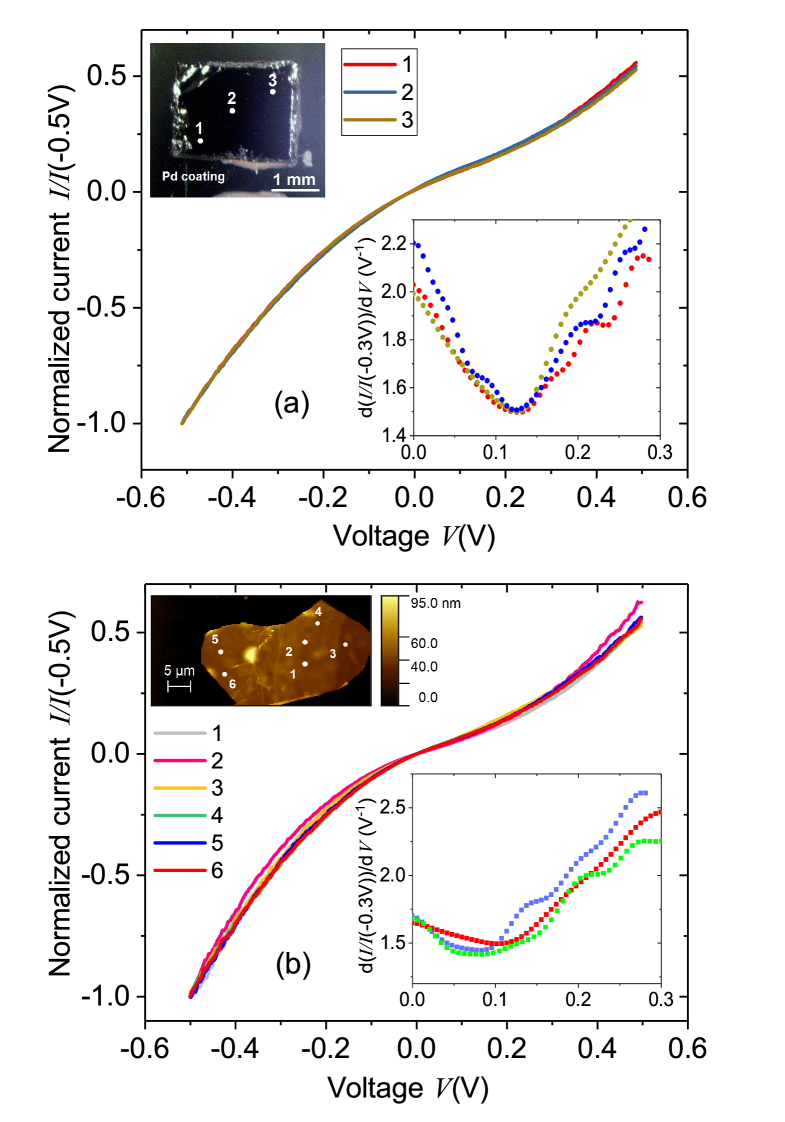
Figure 1 shows the normalized - characteristics and their first derivatives (see insets) for the bulk HOPG sample (a) and a graphite flake (b). Raman spectroscopy indicates that the main phase in those samples is the 2H phase. Figure 1(a) illustrates normalized - curves of the bulk samples, measured at three different spatial positions. All three curves are nearly identical. Analogous measurements on the thin graphite flakes reveal similar curves as for the bulk sample, although with somewhat larger local variations, as depicted in Fig. 1(b). These small spatial variations of the current can be observed in general for thin graphite flakes and are not necessarily related to the presence of SF at the surface but due to bending or defective regions.
Our normalized - curves are asymmetric and the first derivative of the normalized current exhibits a minimum at 0.12 V, see the inset in Fig. 1(a). An early STM work on graphite at ambient conditions reported a relatively wide minimum at low voltages in the differential conductance.Agrait et al. (1992) Similar curves were obtained at 4.2 K on very thin graphene multilayer samples with the Bernal phasePierucci et al. (2015).
At first view, the normalized - curves in Fig. 1 exhibit apparently no band gap, i.e. a voltage region without detectable tunneling current. On the other hand, the first derivative is a quantity generally assumed to be proportional to the LDOS. Although in a classical semiconductor model a minimum in the LDOS can be a trace of a band gap, it is not a sufficient criteria to infer its existence. The simulation of the spectra proposed below can help to discern to which extent the existence of a (small) energy gap is compatible with the measured spectra.
II.1.2 Simulation of the spectra
In view of the aforementioned difficulties that prevent a direct observation of a band gap using the - curves, we turn to a different approach: First, we assume that graphite behaves like an ordinary semiconductor. Under this assumption, a software package, specifically designed for simulating tunneling currents at semiconductor surfaces,Schnedler et al. (2015a, 2016) is employed to investigate the influence of the size of the band gap on the - curves. By comparing simulated - curves with those experimentally obtained on graphite with Bernal stacking, we conclude that the measured spectra can be understood using an ordinary semiconductor model by assuming small band gaps. Finally we try to estimate the size of the band gap from the TUNA measurements.
In order to derive the tunneling current, we follow the two-step method as described in Refs. Schnedler et al. (2015a, 2016) : First, we performed self-consistent electrostatic simulations of the tip-vacuum-semiconductor system to unravel the potential- and carrier distributions in three dimensions. A Pt-Ir tip with a radius of 100 nm and opening angle of 45 ∘ was chosen. The carrier concentrations of the sample are derived using the parabolic band approximation (see, e,g, Ref. Rozplocha et al. (2007)). Band gaps ranging from 0.1 meV to 120 meV are assumed. The graphite’s Fermi-level position as well as the concentration of free electrons and holes at a temperature of K are defined by solving the charge neutrality condition:
| (1) |
with and being the acceptor and donor concentrations. Several Hall effect resultsKinchin (1953); Mrozowski and Chaberski (1956); Soule (1958); Cooper et al. (1970); Brandt et al. (1974); Oshima et al. (1982); Bunch et al. (2005); Vansweevelt et al. (2011); Esquinazi et al. (2014) suggest that graphite should be degenerated with a Fermi-level located inside the valence band with a free carrier concentration of the order of cm-3 at 300 K.Esquinazi et al. (2014); Dusari et al. (2011) We assume density of states effective masses of the order of one hundredth of the electron rest mass for a parabolic band approximation. Using these constraints, we can solve the charge neutrality condition only, if a certain concentration of shallow acceptor states are incorporated. Due to the lack of the precise knowledge about the graphite density of states effective masses and acceptor ionization energies, it remains to be clarified in a future work, whether the assumed concentration of shallow acceptors states depends on the concentration of atomic lattice defects in our HOPG samples. Note that those defects can play a role in the effective carrier density, as irradiation studies indicate.Arndt et al. (2009)
Without bias (), the contact potential is defined as the work function difference between the metallic probe tip (Pt80-Ir20) and the graphite sample. It affects the tip-induced band bending in the same manner like the application of a bias voltage. For Pt and Ir work function values between 5.7 and 5.8 eV were reportedKaack and Fick (1995). On the other hand for graphite the work function varies from 4.6Krishnan and Jain (1952) to 4.7 eVRut’kov et al. (2020). Taking into account these values, the contact potential between the probe tip and graphite surface is expected to be eV.
In a second step, we use the one dimensional electrostatic potential along the central axis through the tip apex to derive the tunneling currents through the vacuum barrier using the WKB approximation based model described in Refs.Bono and Good (1986); Feenstra and Stroscio (1987) . In order to fit the measured - curves to the calculated ones, we took the band gap, the effective masses, the concentration of acceptors and the tip-sample separation as fit parameters.
II.1.3 Modeling of the tunneling current based on the tip-induced band bending
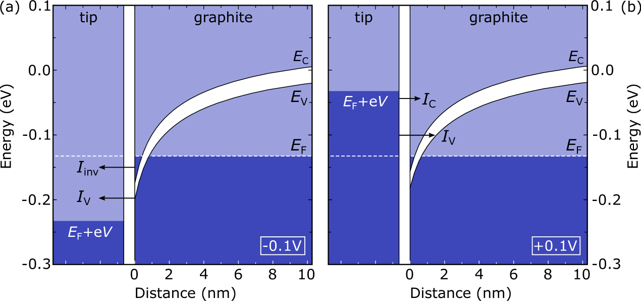
As discussed above, from experiments we expect a free carrier concentration of the order of cm-3 (i.e. cm-2 per graphene layer) at 300 K for Bernal graphite. For such a carrier concentration the electrostatic potential, present between the metallic probe tip and graphite during STM experiments, cannot be screened completely at the graphite surface and can reach the subsurface region of the material (commonly referred to as tip-induced band bending). We take the tip-induced band banding into account in our self-consistent simulations.
The above discussed contact potential of eV in conjunction with small band gaps lead to empty and filled states, which are simultaneously present in both, valence- and conduction-band. Hence, at negative bias (sample) voltages the tunneling out of filled valence- and conduction-band states into empty tip states occurs, while at positive voltages, tunneling from filled tip states into empty valence- and conduction-band states takes place. This situation is illustrated in Fig. 2. Even at positive sample voltages, the downward band bending remains present. In contrast to other -type semiconductors with larger band gaps, tunneling into empty conduction band states () occurs even for very small positive sample voltages already (in addition to the tunneling current into empty valence band states). At a sample voltage of approximately V the increasing becomes larger than the decreasing , leading to the above discussed minimum in the first derivative .
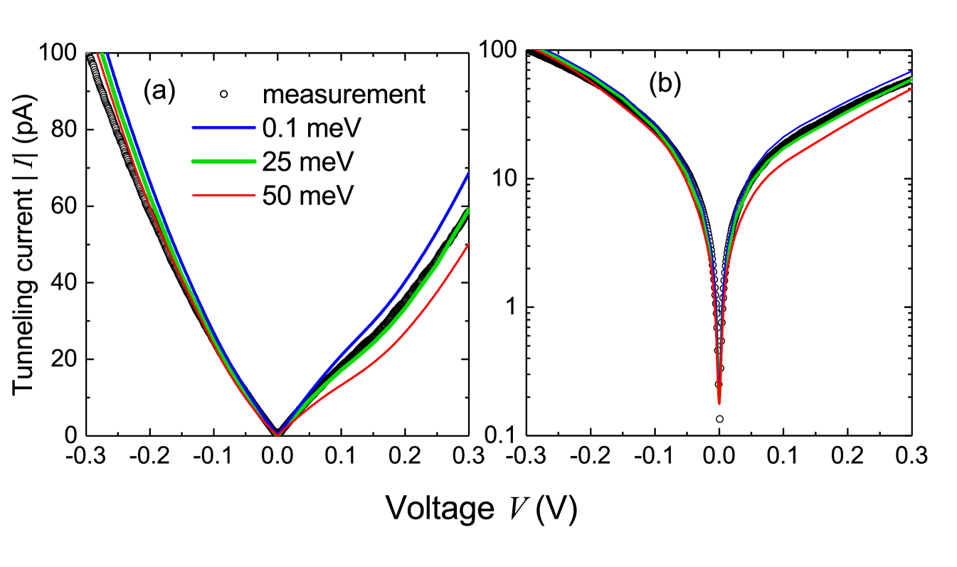
A good agreement between the measured and simulated - curves at Bernal stacked graphite surfaces was achieved as indicated by the green solid line in Fig. 3. This simulation was obtained for a free carrier concentration of cm-3, similar to the expected oneEsquinazi et al. (2014); Dusari et al. (2011), a band gap of 25 meV, similar to that obtained from transport resultsGarcía et al. (2012); Zoraghi et al. (2017), as well as effective masses of 0.01 and 0.0075 for the valence- and conduction-band, respectively. We restricted the calculations within the voltage range of interest V. In the same figure we show the simulations obtained with the same parameters but for band gaps 0.1 meV and 50 meV.
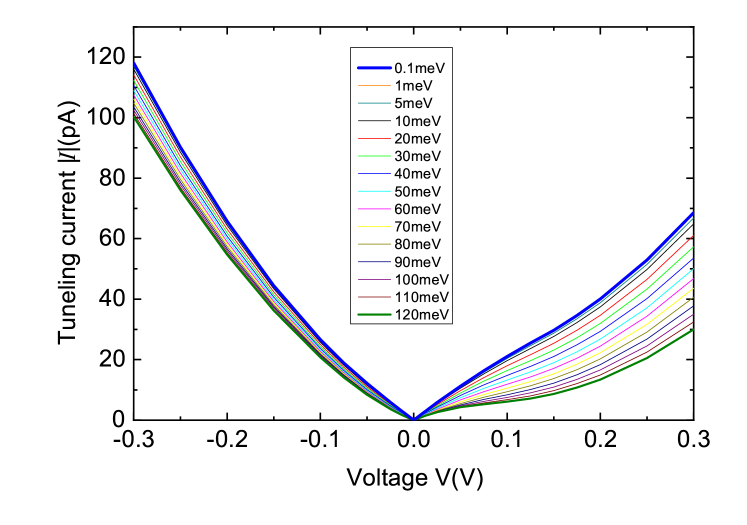
In order to investigate the influence of a band gap on the tunneling spectra of graphite, we calculated - curves for band gaps between 0.1 meV and 120 meV. Figure 4 shows that in particular the tunneling current at the positive voltage branch decreases with increasing band gap. This behavior is caused by an interplay of two effects: First, the shift of the graphite’s conduction band states towards larger energies with increasing band gap leads to less conduction band states that are available for tunneling. Second, a larger band gap leads to an energetically increased tunneling barrier between tip and sample, which in return decreases the tunneling probability. Hence, also the tunneling current related to valence band states decreases slightly with increasing band gap. This delicate interplay alters the slope of the combined tunneling current (i.e. the sum of conduction- and valence-band related tunneling currents) at positive sample voltages and defines the position of the minimum of the curves. Larger band gaps result in stronger curvatures at the positive voltage branch, while for small band gaps the positive voltage branch becomes more linear. In the limit of a vanishing band gap, the minimum in the curve is still present. Note that thermal broadening of the Fermi-Dirac distribution of the Pt80Ir20-tip states is not taken into account in the tunneling current computation, which can however be anticipated to not change the position of the minimum in the curve but only its intensity.
Although the simulations with smaller and larger band gap appear to agree less with the experimental data according to the depicted graph vs. shown in Fig. 3, a clear distinction is difficult on this basis alone. A more sensitive way is given by comparing the first derivative and in particular the position of its minimum. The reason is that the minimum in the curve is found to shift with the band gap as illustrated in Figs. 5(a) and (b). As one can recognize in this graph, the first derivative of one of the curves obtained for sample HOPG-Pd-1 as example (see Fig. 1(a)), roughly agrees with the simulation with energy gap of 25 meV with a minimum at mV. We further quantified the voltage position of the experimentally observed minima by fitting a polynomial of 9th grade to the numerical differentiation of all curves, yielding an average value of mV. The experimental region of the minimum is shown as shadowed area in Fig. 5(b). The comparison of the measured values with the simulated vs. the band gap suggests that the experimental data can be described best with a semiconductor model with a band gap between 12 meV and 37 meV. From the simulated , see Fig. 5(b), we note that the data obtained for the mesoscopic graphite sample with Bernal stacking order, see Fig.1(b), suggest that larger and a broader distribution of band gaps could be localized at certain regions of the inhomogeneous or bended graphite surface. We may speculate that atomic lattice defects, other than simple SF, but twisted or turbostratic stacking with more complexes sequences may have different band gaps.
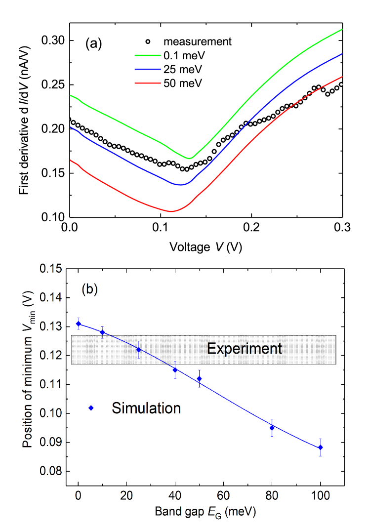
We varied the parameters of the simulations to estimate the error range. A decrease of the contact potential leads to a slight increase of the band gap (meV per 0.1 eV decrease) while decreasing the free carrier concentration ( cm-3 per 0.1 eV decrease) and the effective band masses. Taking into account transport data,Esquinazi et al. (2014); Dusari et al. (2011) we expect that the carrier concentration is at least cm-3 at 300 K. Hence, the contact potential should be eV, which restricts the band gap to meV. Taking into account correlation effects between the parameters, we estimate an error in the carrier density parameter of cm-3. We note that if we assume a negligible band gap at contact potentials smaller than 1 eV, the deviation between the measured data and the theoretical curve increases, pointing further to the existence of a finite energy gap.
We conclude this section by pointing out that the measured spectra for the Bernal stacking order are best described by a semiconductor model with a narrow band gap. In first approximation the first derivative spectra is proportional to the LDOS, although the voltage scale is shifted by the existence of a tip-induced band bending. Taking advantage of these insights in the interpretation of the tunneling spectra on Bernal stacking order graphite, we now turn to measurements of the rhombohedral stacking order of graphite.
II.2 Rhombohedral stacking order
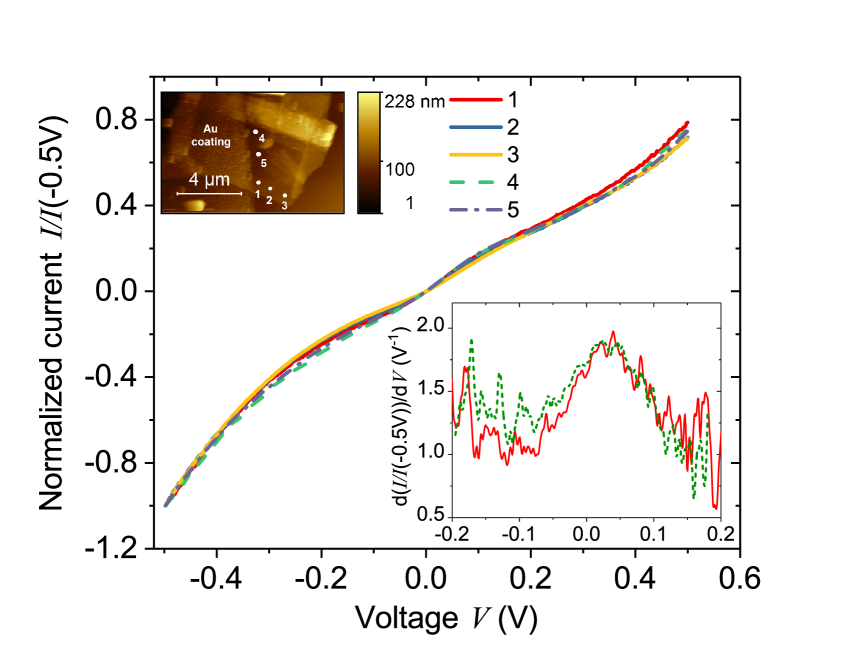
The 3R phase is of especial interest nowadays due to the expected flat band at its surface or at its interfaces with the 2H stacking orderKopnin et al. (2013); Muñoz et al. (2013). A flat band in the 3R phase has been found experimentallyXu et al. (2015); Pierucci et al. (2015); Henck et al. (2018); Wang et al. (2018), which correlates with a maximum in the DOS at the Fermi level, enhancing the probability to trigger superconductivity Kopnin et al. (2013); Heikkilä and Volovik (2016); Volovik (2018) and/or magnetismPamuk et al. (2017); Henck et al. (2018); Ojajärvi et al. (2018) at high temperatures. In particular, STS obtained on a sequence of five layers of 3R phase showed a peak in the DOS around the Fermi level with a width of meV at half maximumPierucci et al. (2015). We have performed TUNA measurements in several natural graphite samples with the 3R phase. For a relatively thick (22 nm) sample with the 3R phase, we measured a clear maximum in the differential conductance reproducible at different positions spread by several m2 in the sample area, see Fig. 6. This maximum is not observed, however, in a 3R phase sample of much smaller thickness (3 nm), see Fig. 7. This difference may indicate that either the roughness of the samples plays a detrimental role or the number of 3R unit cells in the thin sample is not enough to clearly develop this feature at room temperature, as numerical simulations suggest.Kopnin et al. (2013)
We note that the maximum in the differential conductance observed in the thicker 3R sample is shifted by meV above the zero level and with a width at half maximum of meV. Those values are of the same order as reported at 4.2 K, in spite of times higher temperatures, stressing the robustness of the high DOS feature around the Fermi level at the surface of this graphite phase. The shift of the maximum in the differential conductance may come from the influence of a finite contact potential and band bending.
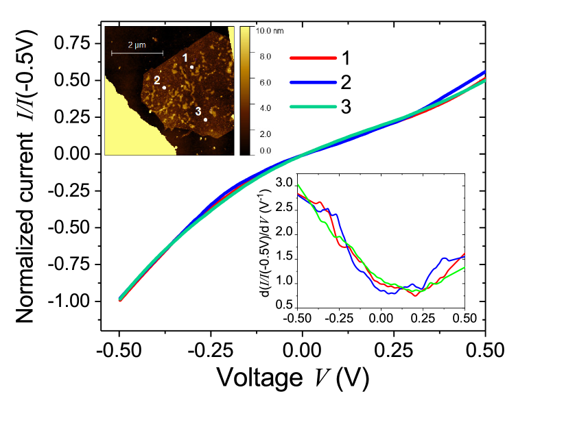
We note that the temperature dependence of the resistance measured for a large number of bulk samples from different origins follows over a very broad range (2 K K) the temperature dependent resistance known for semiconductors, suggesting, that this minority 3R phase should also be a narrow gap semiconductor with an energy gap of the order of 100 meVZoraghi et al. (2017). Under this assumption we would have the situation of a different band structure at the surface from that in the bulk of the 3R phase. The position of the minimum in the first derivative obtained for the thinner samples, see inset in Fig. 7, cannot be determined with sufficient accuracy because it depends very much on the spatial position on the sample. Much better sample quality of thin enough 3R phase samples is necessary to check for a semiconducting behavior with a larger energy gap than in the Bernal case as transport measurements suggestZoraghi et al. (2017). Mean field theoretical studies indicateHyart et al. (2018) that the only possible origin for an energy gap in the bulk of the 3R phase should be related to a spontaneous symmetry breaking, a feature that needs more work to verify its existence.
III Conclusion
Characteristic current-voltage curves obtained by tunneling atomic force spectroscopy (TUNA) on Bernal stacked graphite surfaces can successfully be reproduced by using classical self-consistent semiconductor modeling in conjunction with quantum mechanical tunneling current derivations, taking into account a non-zero band gap as well as reasonable values for the carrier concentration and effective masses of graphite. The best simulation could be obtained for band gaps in the range meV, in agreement with previous transport and Hall-effect studies. The agreement between simulated and measured tunneling currents at 300 K should be considered as a demonstration that the assumption of graphite being a semiconductor with a narrow band gap is in line with the measured data. In particular our model explains the minimum in the curves at mV. It is the result of a delicate interplay of tunnel currents arising from valence- and conduction-band states at both positive and negative sample voltages. Furthermore, we showed that the lack of a voltage region without detectable current in the - spectra, is not sufficient to exclude the presence of a band gap. In analogy, a voltage range without detectable current is not one-to-one equal to the fundamental band gap.Schnedler et al. (2015b); Portz et al. (2017)
In contrast to the results obtained from samples with Bernal stacking, the surface of samples with the rhombohedral stacking order indicate a clear maximum in the differential conductivity, in agreement with previous STS results obtained at much lower temperatures, suggesting the existence of a flat band at the Fermi level. On the other hand, very thin samples with rhombohedral stacking order show a minimum in the first derivative at positive voltages, whose voltage positions depend very much on the sample location.
IV Samples and Methods
IV.1 Samples
The origin, thickness and method for electrical contacts of the measured samples are given in Table 1. The bulk HOPG Grade A sample, from which we prepared the samples HOPGA-Pd-1, MG-Pd-11-1, MG-Pd-11-2 and A1 (see Table I), was obtained from Advanced Ceramics (now Momentive Performance Materials). The total impurity concentration (with exception of H) of the HOPG and natural graphite samples is below 20 ppm, see Refs. Spemann and Esquinazi (2016); Precker et al. (2016) for more details.
| Sample | Thickness (nm) | Origin | Stacking order | Contacts |
|---|---|---|---|---|
| NBF5-01-03 | 22 | Brazil mine | 3R | lithography |
| NBF5-01-05 | 40 | Brazil mine | mixture of 2H and 3R | lithography |
| NBF5-SNG-3 | 3 | Brazil mine | 3R | lithography |
| NBF5-01-09 | 8 | Brazil mine | 2H | lithography |
| HOPGA-Pd-1 | 300 | HOPG Grade A | 2H | Pd-coated |
| MG-Pd-11-1 | 65 | HOPG Grade A | 2H | Pd-coated |
| MG-Pd-11-2 | 40 | HOPG Grade A | 2H | Pd-coated |
| A1 | 45 | HOPG Grade A | 2H | Pd-coated |
Graphite flakes were prepared using a mechanical cleavage. The method consists of mechanically gently rubbing a bulk graphite sample onto a thoroughly cleaned in ethanol substrate. After that, the substrate with the multigraphene flakes is well cleaned in an ultrasonic bath of highly concentrated acetone for one minute several times.
Different ways of electrical contacts fabrication were applied. The investigated graphite samples were placed on top of two differently prepared silicon substrates with a 150 nm thick insulating silicon nitride (Si3N4) couting. On one of the two substrates we patterned electrodes on the samples top surface and on the insulating substrates using electron beam lithography followed by sputtering of a bilayer Cr/Au (5 nm/30 nm). Other graphite samples were electrically contacted by depositing their bottom surface to a 100 nm thick Pd layer sputtered on the Si3N4 coating (after depositing a buffer layer of 31 nm thick Cr).
IV.2 Raman characterization
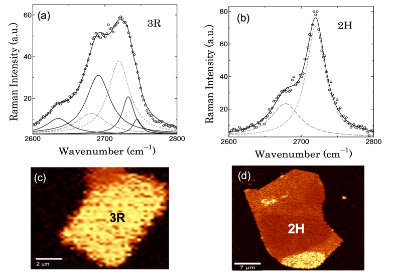
Microscopic analysis of the graphite stacking orders and sample quality were realized by Raman spectroscopy measurements. Raman spectra of multilayer graphene samples were obtained with a confocal micro-Raman microscope WITec alpha 300+ at 532 nm wavelength (green) at ambient temperature, see Fig. 8 as example. All Raman measurements were performed using a grating of 1800 grooves mm-1, 100x objectives (NA 0.9) and incident laser power of 1 mW. Lateral resolution of the confocal micro-Raman microscope was nm and the depth resolution nm.
The Raman results revealed Bernal and rhombohedral stacking orders as well as a mixture of those phases depending on sample. The areas with different stacking orders have been localized by surface scanning and registration of spectra at each point in increments of 100 nm with the confocal micro-Raman microscope. Afterwards, the function of automatic recognition of the given shapes of the spectrum curves showed the regions with different stacking.
Figures 8(a,b) present the Raman spectra in the 2D Raman bands for rhombohedral (3R) area of the NBFG5-01 sample and Bernal (2H) area of the MGPd-11 sample. The spectra are the average obtained by hyperspectral scanning within the respective regions. Figures 8(c,d) show the Raman image that is obtained analyzing the spatial distribution of the 2D band width of the NBF5-01 and MGPd-11 samples. Following recent publications Cong et al. (2011); Henni et al. (2016); Torche et al. (2017); Ramos et al. (2021) there are three main Raman scattering features in rhombohedral stacking order of the graphite structure. The main one that can be used to find the 3R phase is the absorption at the G’-band with a broad peak around cm-1, as shown in Fig. 8(a), in clear contrast to the corresponding peak measured in the 2H phase, see Fig. 8(b). According to the Raman results the investigated samples presented in this study are of high structural quality due to the absence of the disorder-related D-peak around cm-1 (not shown).
These results indicate that while the smaller area in the NBF5-01 sample has a Bernal stacking order, the larger area consists of rhombohedral one. The opposite is observed in the other sample shown in Fig. 8(d).
IV.3 TUNA measurements
Local current-voltage (-) curves measurements were performed with a Bruker Dimension Icon Scanning Probe Microscope equipped with PeakForce Tunneling AFM module (PF-TUNA)Li et al. (2011). The PeakForce Tapping mode is based on a quick contact interaction of the probe and the sample (tens to hundreds of microseconds). PeakForce TUNA mode with a bandwidth of 15 kHz allows the measurement of a current averaged over the full tapping cycle. All measurements were conducted at room temperature and at ambient conditions. Pt-Ir-coated silicon nitride probes with a nominal radius of 25 nm (PF-TUNA, spring constant = 0.4 N/m, resonant frequency = 70 kHz) have been used. PeakForce Tapping Amplitude was set to 150 nm. A current sensitivity of 100 pA/V was used in all measurements. The bias voltage was swept from -500 mV to 500 mV on flat surface regions. In order to decrease the noise in the data, the - curves shown in this study were taken from an average of 25 consecutive - ramps at a single point.
The measurement and calibration of the curves at certain parts of the selected samples were performed as follows: First the curves were measured on a test sample - a floppy disk. After checking the operability, the cantilever was moved to the graphite sample and a nm2 area was scanned in order to localize the flat areas without irregularities. Then a point was chosen in an area of nm2 or nm2 to register the I-V curves. The PeakForce setpoint (trigger force) was chosen as small as possible in order not to damage the surface.
To rule out possible artifacts (e.g., when a piece of graphite sticks at the tip), to check the reproducibility of the measurements and the state of the used Pt-Ir probes, three different tests were used, namely: After each measurement the response of the Pt-Ir probe was examined using the reference sample (FD sample, 12 mm from Bruker). Furthermore, scanning electron microscope (SEM) was used to check for the state of the probes tips. In order to avoid distortion in the data, each probe was used not more than 25 h. After that we continued with a new probe. In the case of the samples with the 3R phase two different probes were used to check for the reproducibility of the unusual behavior at low voltages.
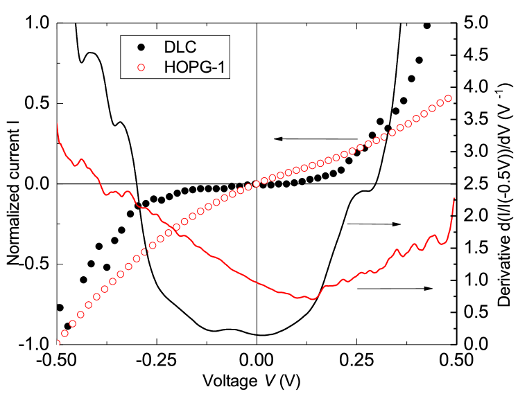
Finally, to verify that the shift of the minima in to positive bias voltages obtained in the graphite samples is not an artifact, we selected a -type semiconducting sample with larger band gap than graphite, but still relatively narrow. Just after measuring one sample with Bernal stacking and without changing the probe or any sets of the microscope, we measured a hydrogenated diamond like carbon (DLC) film, the one usually used in old magnetic hard disks. Upon hydrogenation and defect concentration the energy gap of the DLC films can be as low as a few hundreds of meV. The measured - curve of the DLC film is shown in Fig. 9 together with its differential conductance (right axis). For comparison, in the same figure we include one of the curves obtained from the bulk HOPG sample shown in Fig. 1(a). The - curve of the DLC film and its derivative indicate an energy gap eV. Note that the - curve of the DLC film shows an opposite asymmetry as for graphite, i.e. it is shifted to negative bias voltages.
The TUNA equipment allows in principle a constant current scan to get a scan image of the
conductance variation across the sample surface. This useful tool cannot be easily used for graphite due to
the soft axis elastic module of the graphite structure. When one uses this mode and due to the soft elastic module a
time dependence in the - curves is observed.
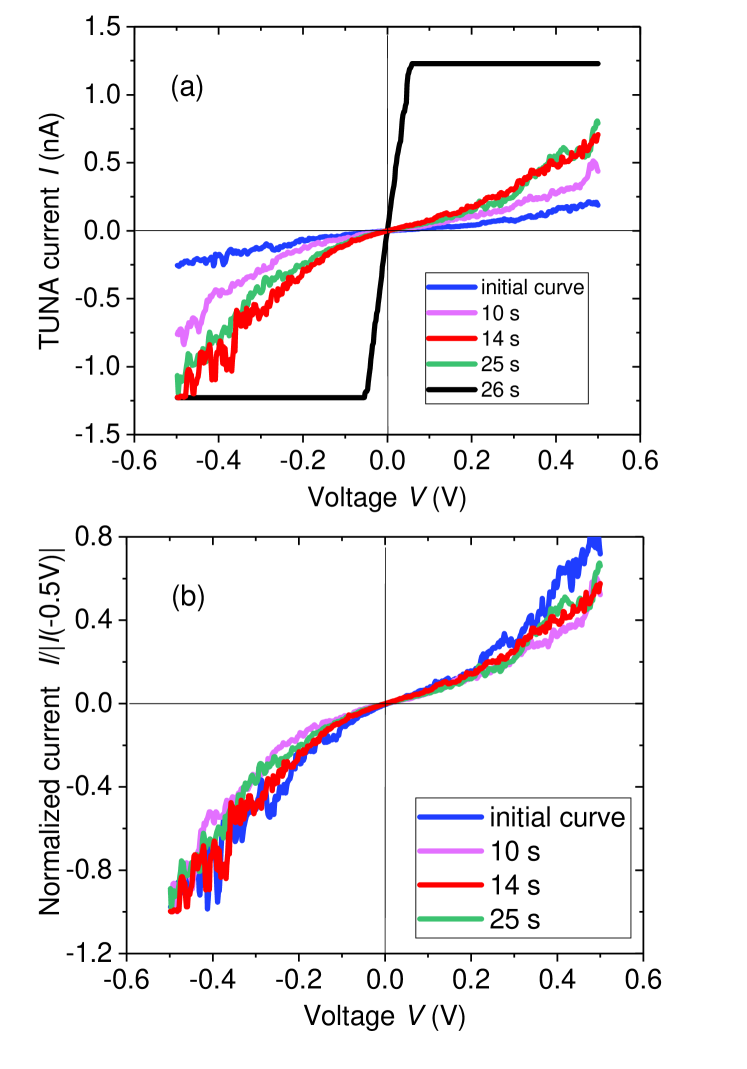
Measurements of the time-dependence of the - spectra were carried out with the graphite sample HOPG-Pd-1
using the spectroscopy mode in the PeakForce TUNA mode.
In order to obtain a series of - curves at one fixed position the Continuous Ramping mode
was used with the parameters: 2 V set point, 100pA/V sensitivity and ramp rate of 1.03 Hz.
The cycle was repeated automatically after certain time. Overall, 26 - curves were obtained within 26 s, some of them
are shown in Fig. 10. These measurements indicate a variation of the tunneling current with time. The observed behavior
is similar to the one observed from tunneling regime to point-contact changing the tip-sample distance in Ref. Agrait et al. (1992).
In the tunneling regime, i.e. at low enough current amplitudes and
before a direct contact is achieved, all - curves
show the same behavior after normalization, see Fig. 10(b).
This effect should be taken into account when measuring electrical characteristics of soft
materials with PF-TUNA mode.
From the technical point of view, the obtained results indicate that the TUNA technique
allows spectroscopy studies in natural and pyrolytic
graphite samples. Care must be taken with time dependent effects due to the soft
axis module of graphite and the set-point selected in the TUNA electronics.
Author Contributions: R.A. carried out the TUNA measurements.
R.A. and A.C. carried out the sample preparation. T.V. and I.E-L. performed
the Raman measurements. A.C. and R.A. contributed to the interpretation of the Raman results. M.Sc. contributed to the interpretation of the results and
performed all numerical studies. W.H., R.E.D-B. and P.E. contributed to the interpretation of the results.
M.St. helped in the measurements and purchasing the microscope with all the used options.
P.D.E. conceived and planned the experiments. P.D.E. and M.Sc. took the lead in writing the manuscript.
All authors provided critical feedback and helped shape the research, analysis, and manuscript.
The authors declare no competing financial interest.
Acknowledgement: The author P.D.E. thanks Tero Heikkilä, Francesco Mauri, Vladimir Volovik, Jose-Gabriel Rodrigo, Andrei Pavlov and Eberhard K. U. Gross for fruitful discussions. We thank Laetitia Bettmann for her help during the studies. This work has been possible with the support of the Saechsischen Aufbaubank (SAB) and the European Regional Development Fund, Grant Nr.: 231301388. A.C. acknowledges 2MI and VRS Eireli Research & Development for the financial support and Nacional do Grafite, MG (Brasil), for the samples.
References
- Zhang et al. (2010) F. Zhang, H. Min, M. Polini, and A. H. MacDonald, Phys. Rev. B 81, 041402 (2010).
- García et al. (2012) N. García, P. Esquinazi, J. Barzola-Quiquia, and S. Dusari, New Journal of Physics 14, 053015 (2012).
- Kelly (1981) B. T. Kelly, Physics of Graphite (London: Applied Science Publishers, 1981).
- Lin et al. (2012) Q. Lin, T. Li, Z. Liu, Y. Song, L. He, Z. Hu, Q. Guo, and H. Ye, Carbon 50, 2369 (2012).
- Precker et al. (2016) C. E. Precker, P. D. Esquinazi, A. Champi, J. Barzola-Quiquia, M. Zoraghi, S. Muiños-Landin, A. Setzer, W. Böhlmann, D. Spemann, J. Meijer, T. Muenster, O. Baehre, G. Kloess, and H. Beth, New J. Phys. 18, 113041 (2016).
- Barzola-Quiquia et al. (2008) J. Barzola-Quiquia, J.-L. Yao, P. Rödiger, K. Schindler, and P. Esquinazi, phys. stat. sol. (a) 205, 2924 (2008).
- Ballestar et al. (2013) A. Ballestar, J. Barzola-Quiquia, T. Scheike, and P. Esquinazi, New J. Phys. 15, 023024 (2013).
- Scheike et al. (2013) T. Scheike, P. Esquinazi, A. Setzer, and W. Böhlmann, Carbon 59, 140 (2013).
- Ballestar et al. (2015) A. Ballestar, P. Esquinazi, and W. Böhlmann, Phys. Rev. B 91, 014502 (2015).
- Esquinazi and Lysogorskiy (2016) P. D. Esquinazi and Y. Lysogorskiy, “Experimental evidence for the existence of interfaces in graphite and their relation to the observed metallic and superconducting behavior,” (P. Esquinazi (ed.), Springer International Publishing AG Switzerland, 2016) Chap. 7, pp. 145–179.
- Zoraghi et al. (2018) M. Zoraghi, J. Barzola-Quiquia, M. Stiller, P. D. Esquinazi, and I. Estrela-Lopis, Carbon 139, 1074 (2018).
- Precker et al. (2019) C. E. Precker, J. Barzola-Quiquia, P. D. Esquinazi, M. Stiller, M. K. Chan, M. Jaime, Z. Zhang, and M. Grundmann, Advanced Engineering Materials 21, 1970039 (2019).
- Kuwabara et al. (1990) M. Kuwabara, D. R. Clarke, and A. A. Smith, Appl. Phys. Lett. 56, 2396 (1990).
- Flores et al. (2013) M. Flores, E. Cisternas, J. Correa, and P. Vargas, Chemical Physics 423, 49 (2013).
- Miller et al. (2010) D. L. Miller, K. D. Kubista, G. M. Rutter, M. Ruan, W. A. de Heer, P. N. First, and J. A. Stroscio, Phys. Rev. B 81, 125427 (2010).
- Brihuega et al. (2012) I. Brihuega, P. Mallet, H. González-Herrero, G. T. de Laissardière, M. M. Ugeda, L. Magaud, J. M. Gómez-Rodríguez, F. Ynduráin, and J.-Y. Veuillen, Phys. Rev. Lett. 109, 196802 (2012).
- Lu et al. (2006) Y. Lu, M. Muñoz, C. S. Steplecaru, C. Hao, M. Bai, N. García, K. Schindler, and P. Esquinazi, Phys. Rev. Lett. 97, 076805 (2006), see also the comment by S. Sadewasser and Th. Glatzel, Phys. Rev. Lett. 98, 269701 (2007) and the reply by Lu et al., idem 98, 269702 (2007) and also R. Proksch, Appl. Phys. Lett. 89, 113121 (2006).
- McClure (1956) J. W. McClure, Phys. Rev. 104, 666 (1956).
- Semenenko and Esquinazi (2018) B. Semenenko and P. Esquinazi, Magnetochemistry 4, 52 (2018).
- McClure (1957) J. W. McClure, Physical Review 108, 612 (1957).
- Slonczewski and Weiss (1958) J. C. Slonczewski and P. R. Weiss, Physical Review 109, 272 (1958).
- McClure (1958) J. W. McClure, Physical Review 112, 715 (1958).
- Cao et al. (2018) Y. Cao, V. Fatemi, S. Fang, K. Watanabe, T. Taniguchi, E. Kaxiras, and P. Jarillo-Herrero, Nature 556, 43 (2018).
- Marchenko et al. (2018) D. Marchenko, D. V. Evtushinsky, E. Golias, A. Varykhalov, T. Seyller, and O. Rader, Science Advances 4 (2018), 10.1126/sciadv.aau0059.
- Ballestar et al. (2014) A. Ballestar, T. T. Heikkilä, and P. Esquinazi, Superc. Sci. Technol. 27, 115014 (2014).
- Esquinazi et al. (2018) P. D. Esquinazi, C. E. Precker, M. Stiller, T. R. S. Cordeiro, J. Barzola-Quiquia, A. Setzer, and W. Böhlmann, Quantum Studies: Mathematics and Foundations 5, 41 (2018).
- Zoraghi et al. (2017) M. Zoraghi, J. Barzola-Quiquia, M. Stiller, A. Setzer, P. Esquinazi, G. Kloess, T. Muenster, T. Lühmann, and I. Estrela-Lopis, Phys. Rev. B 95, 045308 (2017).
- Barzola-Quiquia et al. (2019) J. Barzola-Quiquia, P. D. Esquinazi, C. E. Precker, M. Stiller, M. Zoraghi, T. Förster, T. Herrmannsdörfer, and W. A. Coniglio, Phys. Rev. Materials 3, 054603 (2019).
- Kinchin (1953) G. H. Kinchin, Proc. R. Soc. Lond. A 217, 1128 (1953).
- Mrozowski and Chaberski (1956) S. Mrozowski and A. Chaberski, Phys. Rev. 104, 74 (1956).
- Soule (1958) D. E. Soule, Phys. Rev. 112, 698 (1958).
- Cooper et al. (1970) J. D. Cooper, J. Woore, and D. A. Young, Nature 721–722, 225 (1970).
- Brandt et al. (1974) N. B. Brandt, G. A. Kapustin, V. G. Karavaev, A. S. Kotosonov, and E. A. Svistova, Sov. Phys.-JETP 40, 564 (1974).
- Oshima et al. (1982) H. Oshima, K. Kawamura, T. Tsuzuku, and K. Sugihara, J Phys. Soc. Japan 51, 1476 (1982).
- Bunch et al. (2005) J. S. Bunch, Y. Yaish, M. Brink, K. Bolotin, and P. L. McEuen, Nano Letters 5, 287 (2005).
- Vansweevelt et al. (2011) R. Vansweevelt, V. Mortet, J. D’Haen, B. Ruttens, C. V. Haesendonck, B. Partoens, F. M. Peeters, and P. Wagner, Phys. Status Solidi A 208, 1252 (2011).
- Kopelevich et al. (2003) Y. Kopelevich, J. H. S. Torres, R. R. da Silva, F. Mrowka, H. Kempa, and P. Esquinazi, Phys. Rev. Lett. 90, 156402 (2003).
- Kempa et al. (2006) H. Kempa, P. Esquinazi, and Y. Kopelevich, Solid State Communications 138, 118 (2006).
- Kopelevich et al. (2006) Y. Kopelevich, J. M. Pantoja, R. da Silva, F. Mrowka, and P. Esquinazi, Phys. Lett. A 355, 233 (2006).
- Schneider et al. (2009) J. M. Schneider, M. Orlita, M. Potemski, and D. K. Maude, Phys. Rev. Lett. 102, 166403 (2009), see also the comment by I. A. Luk’yanchuk and Y. Kopelevich, idem 104, 119701 (2010).
- Esquinazi et al. (2014) P. Esquinazi, J. Krüger, J. Barzola-Quiquia, R. Schönemann, T. Hermannsdörfer, and N. García, AIP Advances 4, 117121 (2014).
- Breusing et al. (2009) M. Breusing, C. Ropers, and T. Elsaesser, Phys. Rev. Lett. 102, 086809 (2009).
- Sugawara et al. (2007) K. Sugawara, T. Sato, S. Souma, T. Takahashi, and H. Suematsu, Phys. Rev. Lett. 98, 036801 (2007).
- Grüneis et al. (2008) A. Grüneis, C. Attaccalite, T. Pichler, V. Zabolotnyy, H. Shiozawa, S. L. Molodtsov, D. Inosov, A. Koitzsch, M. Knupfer, J. Schiessling, R. Follath, R. Weber, P. Rudolf, R. Wirtz, and A. Rubio, Phys. Rev. Lett. 100, 037601 (2008).
- Liu et al. (2010) Y. Liu, L. Zhang, M. K. Brinkley, G. Bian, T. Miller, and T.-C. Chiang, Phys. Rev. Lett. 105, 136804 (2010).
- Yin et al. (2020) R. Yin, Y. Zheng, X. Ma, Q. Liao, C. Ma, and B. Wang, Phys. Rev. B 102, 115410 (2020).
- González et al. (2007) J. C. González, M. Muñoz, N. García, J. Barzola-Quiquia, D. Spoddig, K. Schindler, and P. Esquinazi, Phys. Rev. Lett. 99, 216601 (2007).
- Henck et al. (2018) H. Henck, J. Avila, Z. Ben Aziza, D. Pierucci, J. Baima, B. Pamuk, J. Chaste, D. Utt, M. Bartos, K. Nogajewski, B. A. Piot, M. Orlita, M. Potemski, M. Calandra, M. C. Asensio, F. Mauri, C. Faugeras, and A. Ouerghi, Phys. Rev. B 97, 245421 (2018).
- Li et al. (2011) C. Li, S. Minne, B. Pittenger, and A. Mednick, “Simultaneous Electrical and Mechanical Property Mapping at the Nanoscale with PeakForce TUNA,” (2011), bruker Application Note #132 (2011).
- Pierucci et al. (2015) D. Pierucci, H. Sediri, M. Hajlaoui, J.-C. Girard, T. Brumme, M. Calandra, E. Velez-Fort, G. Patriarche, M. G. Silly, G. Ferro, V. Souliere, M. Marangolo, F. Sirotti, F. Mauri, and A. Ouerghi, ACS Nano 9, 5432 (2015).
- Kopnin et al. (2013) N. B. Kopnin, M. Ijäs, A. Harju, and T. T. Heikkilä, Phys. Rev. B 87, 140503 (2013).
- Volovik (2018) G. E. Volovik, JETP Letters 107, 516 (2018).
- Cong et al. (2011) C. Cong, T. Yu, K. Sato, J. Shang, R. Saito, G. F. Dresselhaus, and M. S. Dresselhaus, ACS Nano 5, 8760 (2011), https://doi.org/10.1021/nn203472f .
- Henni et al. (2016) Y. Henni, H. P. O. Collado, K. Nogajewski, M. R. Molas, G. Usaj, C. A. Balseiro, M. Orlita, M. Potemski, and C. Faugeras, Nano Letters 16, 3710 (2016).
- Torche et al. (2017) A. Torche, F. Mauri, J.-C. Charlier, and M. Calandra, Phys. Rev. Materials 1, 041001 (2017).
- Ramos et al. (2021) S. L. L. Ramos, M. A. Pimenta, and A. Champi, Carbon (2021), https://doi.org/10.1016/j.carbon.2021.01.154.
- Agrait et al. (1992) N. Agrait, J. Rodrigo, and S. Vieira, Ultramicroscopy 42 – 44, Part 1, 177 (1992).
- Schnedler et al. (2015a) M. Schnedler, V. Portz, P. H. Weidlich, R. E. Dunin-Borkowski, and Ph. Ebert, Phys. Rev. B 91, 235305 (2015a).
- Schnedler et al. (2016) M. Schnedler, R. E. Dunin-Borkowski, and Ph. Ebert, Phys. Rev. B 93, 195444 (2016).
- Rozplocha et al. (2007) F. Rozplocha, J. Patyk, and J. Stankowski, Acta Physica Polonica A 112 (2007), http://przyrbwn.icm.edu.pl/APP/PDF/112/a112z308.pdf .
- Dusari et al. (2011) S. Dusari, J. Barzola-Quiquia, P. Esquinazi, and N. García, Phys. Rev. B 83, 125402 (2011).
- Arndt et al. (2009) A. Arndt, D. Spoddig, P. Esquinazi, J. Barzola-Quiquia, S. Dusari, and T. Butz, Phys. Rev. B 80, 195402 (2009).
- Kaack and Fick (1995) M. Kaack and D. Fick, Surface Science 342, 111 (1995).
- Krishnan and Jain (1952) K. Krishnan and S. Jain, Nature 169, 702 (1952).
- Rut’kov et al. (2020) E. Rut’kov, E. Afanas’eva, and N. Gall, Diamond and Related Materials 101, 107576 (2020).
- Bono and Good (1986) J. Bono and R. H. Good, Surf. Sci. 175, 415 (1986).
- Feenstra and Stroscio (1987) R. M. Feenstra and J. A. Stroscio, J. Vac. Sci. Technol. B 5, 923 (1987).
- Muñoz et al. (2013) W. A. Muñoz, L. Covaci, and F. Peeters, Phys. Rev. B 87, 134509 (2013).
- Xu et al. (2015) R. Xu, L.-J. Yin, J.-B. Qiao, K.-K. Bai, J.-C. Nie, and L. He, Phys. Rev. B 91, 035410 (2015).
- Wang et al. (2018) W. Wang, Y. Shi, A. A. Zakharov, M. Syväjärvi, R. Yakimova, R. I. G. Uhrberg, and J. Sun, Nano Letters 18, 5862 (2018), https://doi.org/10.1021/acs.nanolett.8b02530 .
- Heikkilä and Volovik (2016) T. Heikkilä and G. E. Volovik, “Flat bands as a route to high-temperature superconductivity in graphite,” (P. Esquinazi (ed.), Springer International Publishing AG Switzerland, 2016) pp. 123–144.
- Pamuk et al. (2017) B. Pamuk, J. Baima, F. Mauri, and M. Calandra, Phys. Rev. B 95, 075422 (2017).
- Ojajärvi et al. (2018) R. Ojajärvi, T. Hyart, M. A. Silaev, and T. T. Heikkilä, Phys. Rev. B 98, 054515 (2018).
- Hyart et al. (2018) T. Hyart, R. Ojajärvi, and T. Heikkilä, J. Low Temp Phys 191, 35 (2018), https://doi.org/10.1007/s10909-017-1846-3 .
- Schnedler et al. (2015b) M. Schnedler, V. Portz, H. Eisele, R. E. Dunin-Borkowski, and Ph. Ebert, Phys. Rev. B 91, 205309 (2015b).
- Portz et al. (2017) V. Portz, M. Schnedler, L. Lymperakis, J. Neugebauer, H. Eisele, J.-F. Carlin, R. Butté, N. Grandjean, R. E. Dunin-Borkowski, and P. Ebert, Appl. Phys. Lett. 110, 022104 (2017).
- Spemann and Esquinazi (2016) D. Spemann and P. Esquinazi, “Evidence for magnetic order in graphite from magnetization and transport measurements,” (P. Esquinazi (ed.), Springer International Publishing AG Switzerland, 2016) pp. 45–76.