Low Cross-Talk Optical Addressing of Trapped-Ion Qubits Using a Novel Integrated Photonic Chip
Abstract
Individual optical addressing in chains of trapped atomic ions requires generation of many small, closely spaced beams with low cross-talk. Furthermore, implementing parallel operations necessitates phase, frequency, and amplitude control of each individual beam. Here we present a scalable method for achieving all of these capabilities using a novel integrated photonic chip coupled to a network of optical fibre components. The chip design results in very low cross-talk between neighbouring channels even at the micrometre-scale spacing by implementing a very high refractive index contrast between the channel core and cladding. Furthermore, the photonic chip manufacturing procedure is highly flexible, allowing for the creation of devices with an arbitrary number of channels as well as non-uniform channel spacing at the chip output. We present the system used to integrate the chip within our ion trap apparatus and characterise the performance of the full individual addressing setup using a single trapped ion as a light-field sensor. Our measurements showed intensity cross-talk below across the chip, with minimum observed cross-talk as low as .
Introduction
Since their original proposal as a platform for quantum information processing[1], trapped ions have emerged as one of the leading contenders for building a useful quantum computer. To date, small-scale trapped-ion systems have demonstrated the highest single- and two-qubit gate fidelities[2, 3, 4, 5], longest coherence times[6], and lowest state preparation and measurement errors[7] of any quantum computing platform. For realising a functional large-scale quantum computer, this level of control needs to be extended to a large number of qubits. This includes the implementation of all necessary quantum operations on the qubit register with very high fidelity as well as the execution of targeted (addressed) operations on specific subsets of qubits within the register with minimal effect on the unused (idle) qubits in the computation.
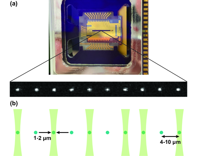
Individual addressing in most types of ion trap quantum computing architectures requires locally modifying the interaction between the ions and the radiation used to perform operations with very low cross-talk, where the natural inter-ion spacing is a few micrometres[8, 9]. This can be done by altering the properties of the magnetic and/or electric fields experienced by each of the ions to change their response to a globally applied field[10, 11, 12, 13, 14, 15], by focusing down the radiation used to perform quantum gates on each ion[16, 17, 18, 19, 20, 21, 22] as shown in fig. 1, or by using a combination of the two approaches. The former approach works with both laser and microwave radiation but requires intricate local control of electric and magnetic fields. Hence it is only compatible with microfabricated traps with numerous electrodes. The latter approach is only viable when optical wavelengths are used for operations, either when the qubit transition is driven with a two-photon Raman process or the qubit transition itself corresponds to an optical wavelength. It requires focusing down laser beams to micrometre scales, therefore working close to the diffraction limit. However, this method is applicable to all ion trap architectures.
Several methods have been developed for achieving individual optical addressing in ion trap systems, including micro-mirror beam steering[16, 17, 18], acousto-optic deflectors[19], multi-channel acousto-optic modulators[20] (AOMs), and micro-lens arrays[21]. These methods vary in cross-talk performance and scalability. Using micro-mirror arrays to steer the lasers onto the target ions offers individual addressing with very low cross-talk. However, the time required to reconfigure the beam positions or to tune the amplitude of the beams is comparable to the timescale of the gate operations, therefore accounting for a significant amount of the sequence run time. Acousto-optic deflectors offer similarly low cross-talk but also enable fast intensity control of the individual beams. However, they lack individual beam frequency control, therefore limiting the set of unitaries that can be implemented in parallel. Furthermore, only a few ions can be addressed at any one time due to power losses in higher diffraction orders. Multi-channel AOMs solve the problem of fast parallel control. However, they exhibit an order of magnitude larger cross-talk compared to the previous two approaches due to electronic cross-talk between channels in existing devices. Additionally, they are only manufactured with a fixed and equal inter-channel spacing, and readily available with only up to 32 channels, limiting both scalability and ability to address non-evenly spaced chains. The micro-lens array approach solves the majority of the problems listed above by enabling parallel operations with very low cross-talk. However, the system presented in ref. 21 has a very high insertion loss limiting the obtainable light intensity at the ion, and a fixed, uniformly spaced output pattern that cannot be easily adapted to non-uniform ion crystals.
In this work, we demonstrate a novel approach to individual optical addressing in trapped-ion chains with minimal cross-talk using a network of fibre-coupled modulators connected to a high-performance photonic chip. We employ spherical phase-induced multiscan waveguides[25] (SPIM-WGs) that provide precise control over the optical mode and enable much higher refractive index (RI) contrast modifications in optical glass compared to conventional ultrafast laser-written waveguides. A similar approach using laser-written waveguide devices has been reported[22], however matching the output of these waveguides to the ion chain while maintaining a good spot quality and low cross-talk is yet to be demonstrated.
The photonic chip that we present here adopts individual adiabatic mode converters as light guiding channels that exhibit excellent optical mode confinement and low cross-talk even at a channel separation of a few micrometres. This ensures that the errors due to nearest-neighbour cross-talk do not limit the performance of the trapped-ion device. Furthermore, the manufacturing process of the SPIM-WGs offers high flexibility, facilitating easy modification of the number of channels, the channel positions, and the mode shapes in the chip design, therefore making the chip easily adaptable to the ion configurations found in most ion trap experiments. The use of a fibre network for light delivery to the photonic chip further simplifies the process of exchanging devices by minimising the necessary realignment, thus allowing for rapid iteration of the system design.
Results
Photonic chip design
Performing laser-driven targeted operations in long chains of trapped ions imposes several competing requirements on the individual addressing setup. First, to minimise errors on the idle qubits, it is crucial to minimise the cross-coupling between neighbouring ion sites. Second, the spacing between neighbouring channels must match the ion-ion spacing, typically on the order of a few micrometres [8, 9]. This requires generating a series of closely spaced beams, each focused to an waist radius as shown in fig. 1(b). As a result, this approach necessitates focusing the beams near the diffraction limit. Working with tightly focused beams can also increase errors in the quantum operations due to intensity, phase, and/or polarisation modulation of the light at the ion position. This modulation can be caused by mechanical drifts in the optical system or by the secular motion of the ions[26, 27]. Hence it is desirable to make the beam waist radius as large as possible. The requirements on the beam spacing and beam waist radius constrain the waist-to-spacing ratio of the device output. A larger ratio makes integration into the trapped-ion system easier and more robust to errors but also increases the cross-talk within the device. Furthermore, to ensure that the required input laser power scales favourably with the qubit register size, it is important to maintain a high throughput efficiency of the system. Finally, the ability to control the intensity, phase, and frequency of individual channels in parallel enables the simultaneous application of different unitary operations on different target qubits, therefore reducing the algorithm run time.
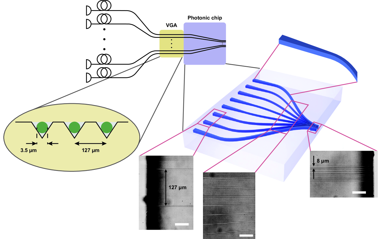
To address these challenges, we developed a novel photonic chip connected to a network of optical fibre components. In our system the source laser is coupled into a series of fibre splitters, such that the light is split up into the required number of channels. Each channel is then connected to a fibre AOM that allows for individual phase, frequency, and amplitude control, and for switching of each beam. The fibre AOMs are connected to a fibre V-groove array (VGA) whose output is an array of fibre cores with a mode field diameter (MFD) of and a uniform spacing of . The VGA is then coupled to the photonic chip as shown in fig. 2 and fixed in place with glue (details in "Materials and methods") to avoid misalignment during operation.
The photonic chip performance benefited from several advanced design and fabrication techniques, as detailed in the following sections. It was designed to convert the input optical modes and spacing of the VGA channels into closely spaced () modes suitable for trapped-ion addressing. Each channel incorporated a high-efficiency adiabatic mode converter to transform the optical mode from the VGA, equivalent to a single-mode fibre (SMF), into the smaller optical mode required to address the ions. The adiabatic mode conversion was implemented over a distance of , starting from the chip’s input facet. Subsequently, curved routing of the channels was used to reduce the channel spacing, while maintaining their cross-sectional shape at the output facet of the chip. The microscopic images in fig. 2 obtained from the top of the photonic chip, capturing the input facet, bending region, and output facet, illustrate the progression of the channel spacing along the chip. Even though the channels were closely stacked with spacing over a distance of , we were able to maintain a low nearest-neighbour cross-talk at a level of as demonstrated in the following sections.
High-contrast refractive index modification
As outlined in the previous section, individual optical addressing of trapped ions requires the generation of closely spaced beams with maximum waist-to-spacing ratio and minimum cross-talk. That way, the errors due to unwanted operations on the idle qubits are minimised, while maximising the robustness of the system. This translates to the need for a very high level of light confinement in the channels of the photonic chip. Existing methods of producing micro-waveguides in photonic chips require a very small waist-to-spacing ratio to satisfy the low cross-talk requirement. An ideal fabrication method would allow an increase in waveguide size while maintaining single-mode operation and low cross-talk. The key to this is a stronger confinement of the mode by increasing the RI contrast between the core and the cladding. This level of RI control has not yet been possible with conventional ultrafast laser writing, where high RI contrast is typically accompanied by poor control of the mode shape.
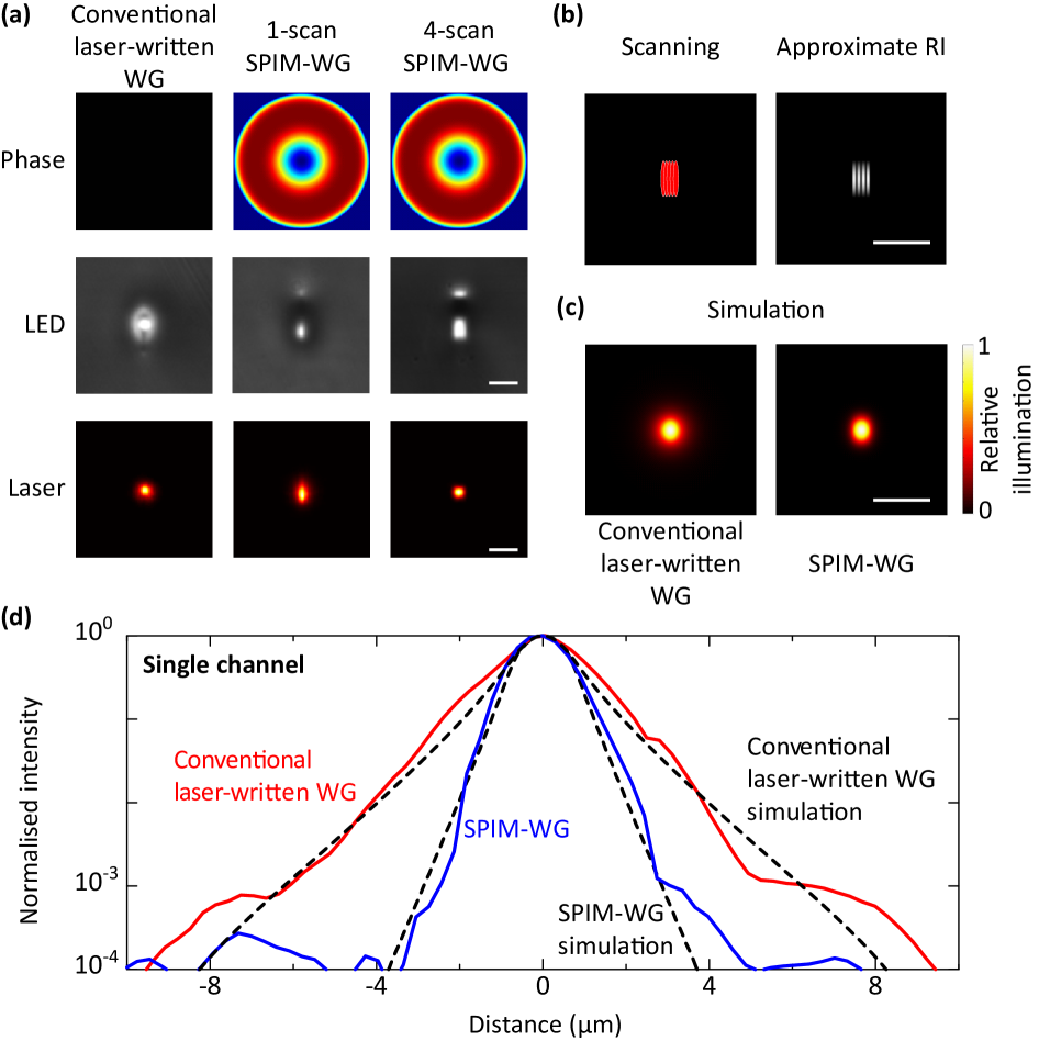
In order to address this challenge, in this work we fabricated SPIM-WGs using a multiscan scheme to precisely control the shape and the size of the channel cross-section, enabling single-mode operation and a large core diameter. To achieve high-precision RI modification, the SPIM-WGs were fabricated with combined spherical aberrations of first-order Zernike mode and third-order Zernike mode introduced into the focused laser[28], with root mean square (RMS) amplitudes of and , respectively. The SPIM-WG design incorporated four scans with a core separation of forming a single light guiding channel. The RI contrast measured using high-resolution quantitative phase microscopy was approximately (with a core RI of and a cladding RI of ), which is two to three times higher than for a waveguide created by conventional ultrafast laser writing[25]. The horizontal core size of one complete SPIM channel was measured to be about , which was approximately the maximum diameter that maintained single-mode operation with an RI contrast of at [29]. Figure 3(a) presents a comparison between LED microscopic images and laser mode profiles for a conventional laser-written waveguide, a single-scan SPIM-WG, and a four-scan SPIM-WG. Figure 3(b) illustrates the scanning scheme and the approximate RI profiles. Additionally, fig. 3(c) shows COMSOL-simulated mode profiles for a conventional laser-written waveguide and a four-scan SPIM-WG. We observed a slight mode elongation along the vertical direction. However, this does not affect the mode quality or the cross-talk in the direction parallel to the ion chain. In fact, it is advantageous for optical addressing of trapped ions, as it improves the robustness of the system to intensity modulation in that direction.
We observed a bright lobe above the four-scan SPIM-WG as shown in fig. 3(a). Such lobes were significantly weaker in the single-scan SPIM-WG. Close examination showed that these lobes possessed a low RI contrast and exhibited high guiding losses. Notably, there was a negative relative RI modification between the main lobe and the upper lobe. In this application, the main lobe was used as the light guiding channel, and we observed no adverse effects arising from the presence of the upper lobe. The strong confinement to the main guiding channel could be attributed to the presence of the region with negative RI contrast between the two lobes, as well as the high transmission loss associated with the upper lobe.
To illustrate the light confinement capabilities, we performed high dynamic range measurements (HDRMs) of the guided laser modes at . Figure 3(d) illustrates measured and simulated HDRMs for a single channel. We observed a close agreement between the simulations and the experiments. A clear difference in the degree of mode confinement was observed between the conventional laser-written waveguide and the SPIM-WG. At distances of from the centre, the intensity from the SPIM-WG was around an order of magnitude lower compared to that of the conventional laser-written waveguides we tested.
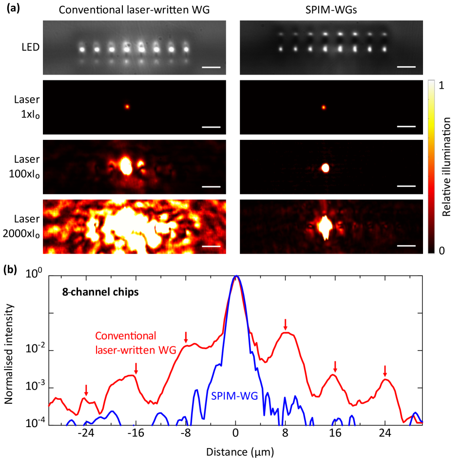
Eight-channel chips were designed according to the specifications outlined in the previous section and illustrated in fig. 2. In fig. 4(a) we show LED microscopic images of the output chip facet. The outer channels appear dimmer than the central channels due to the lower LED intensity away from the centre. We conducted measurements to assess the overall loss (including coupling and propagation losses) across all waveguide channels and found the bending losses in all channels to be negligible, owing to the high RI contrast resulting in a strong mode confinement.
Channel cross-talk was assessed by coupling a laser through a single-mode fibre to one central channel at the chip input facet, then observing the full 8-channel intensity distribution at the chip output. High dynamic range measurements were compiled from a sequence of images taken with different calibrated neutral density filters. As shown in fig. 4(a), the SPIM-WGs showed far better confinement of the laser light to the vicinity of the channel compared to conventional laser-written waveguides. The light intensity at the position of the neighbouring channels, i.e. away from the channel, was one to two orders of magnitude lower for the SPIM-WGs. Further details are provided in fig. 4(b). The red curve, corresponding to conventional laser-written waveguides, clearly shows coupling into the neighbouring channels, evident from the multiple high light intensity peaks at intervals corresponding to the channel separation. In contrast, the SPIM-WGs exhibited minimal coupling to adjacent channels. We measured nearest-neighbour cross-talk of for the conventional laser-written waveguides and for the SPIM-WG channels. These measurements were repeated for multiple different chips, all of which showed consistent results, confirming the high reliability of the chip fabrication.
Advanced mode matching and adiabatic mode conversion
To ensure that the required laser input power to the addressing setup scales favourably with the number of qubits, it is crucial to maintain a high throughput efficiency within the chip-based system. This has been a problem in previous single-ion addressing implementations, where losses of more than have been observed due to poor coupling between system components[21]. The photonic chip must therefore implement high-efficiency coupling between the set of SMFs delivering the light, held in a VGA, to the input of the ion-trap lens system. This can only be achieved through effective mode matching between the components and adiabatic conversion between the modes. Figure 5(a) shows calculated maximum diameters for the waveguide core and guiding mode to maintain single-mode operation for different RI contrasts. Commercial SMFs typically have an MFD of at a wavelength of , while the SPIM-WG channel has a maximum single-mode MFD of along the horizontal direction, owing to the high RI contrast of . Significant coupling losses would arise if the larger SMF modes are coupled directly to the smaller, high RI SPIM-WG channel modes.
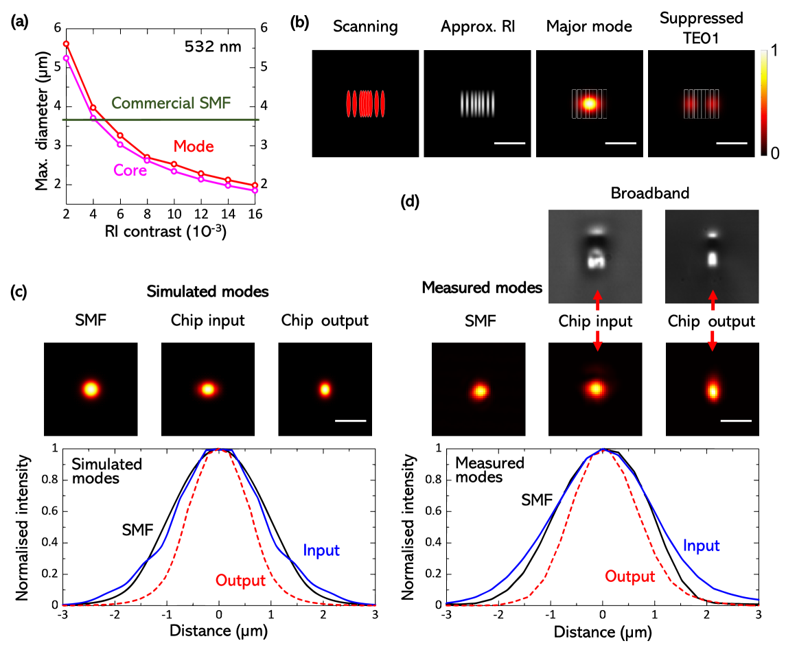
An additional concern relates to position uncertainties in the VGA. The commercial VGAs we used were designed to have a core separation of , but exhibited variable position offsets between the fibre cores of up to along the -direction (parallel to the linear fibre core array) and up to along the -direction (orthogonal to the linear fibre core array). These offsets significantly reduced the mode overlaps between the VGA and the photonic chip and increased the coupling losses.
We developed a novel design for advanced mode matching that effectively mitigates the impact of the VGA channel position variability. The design, presented in fig. 5(b), was built upon the central region of the four scans discussed earlier [fig. 3(b)]. We introduced two additional scans on either side of the 4-scan SPIM-WG in order to increase the lateral size of the waveguide mode. The spacing of these additional scans was times larger than that of the four central scans. As shown in fig. 5(b), this design considerably extended the lateral size of the dominant mode while effectively suppressing higher-order modes (e.g., the TE01 mode). Figure 5(d) includes broadband-light-illuminated microscope images of the channel input and output cross-sections, further highlighting the difference between RI modifications.
Figure 5(c) presents the simulated guiding modes for the SMF, the output channel (as described in the previous section), and the input channel (dominant mode only). The input channel mode was nearly identical to that of the SMF, but considerably larger than that of the output channel. The experimentally measured mode profiles, summarized in fig. 5(d), agreed well with the simulations. The measured mode for the input channel in fig. 5(d) appeared slightly larger than the simulated dominant mode in fig. 5(c) because the measured mode profile contained a superposition of multiple modes, while the simulation included only the dominant mode. Loss measurements indicated that this specialized design enhanced the coupling efficiency from less than to approximately and significantly improved the mode uniformity across the channels.
To address the disparity in cross-section between the channel input mode and the required output mode, we incorporated adiabatic mode conversion by changing the waveguide properties along the chip. Starting from the input facet, the RI profile was gradually changed over a total length of , transitioning from the design illustrated in fig. 5(b) to the design described in fig. 3(b). The RI profile from fig. 3(b) was then maintained throughout the bending region until the chip output. A 3D render of the adiabatic mode conversion is presented in the "Materials and methods" section. The mode conversion efficiency was investigated through measurements of the losses of straight SPIM-WG channels with and without adiabatic mode conversion. Negligible differences in loss were found between the two designs, proving the practical effectiveness of adiabatic mode conversion using SPIM-WGs.
Integration with a trapped-ion quantum system
In our experiment we use trapped ions as qubits. The ions are confined in a 3D monolithic microfabricated trap[23, 24] that allows for generation of deep confining potentials while maintaining low heating rates, which is crucial for storing long ion crystals. The segmented electrode structure provides sufficient degrees of freedom for both ion shuttling across the trap and generation of anharmonic potential shapes. The latter is particularly important for maintaining a uniform ion-ion spacing in large registers[30], therefore increasing the minimum distance between neighbouring ions compared to harmonically spaced chains[8]. As explained in the previous sections, a larger ion-ion spacing reduces the cross-talk between neighbouring channels in the addressing setup.
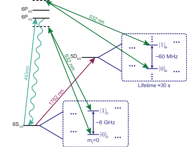
The SPIM-WGs used for individual addressing in our setup were optimised for . This wavelength enables driving Raman transitions within both the ground and the metastable level manifolds of the ions as shown in fig. 6. The output of the photonic chip is mapped on the ion chain using a 2:1 lens relay, such that the distance between neighbouring beams at the ion position is reduced to , matching our target ion spacing.
An outline of the optical system used to reimage the SPIM-WG output on the ions is shown in fig. 7. The output of the chip is collimated using a high-quality commercial microscope objective to minimise aberrations. Another microscope objective is used to both refocus the control light from the waveguide on the ions, and to collect the photons scattered by the ions. The latter objective is chromatically corrected for visible wavelengths, and glass-thickness compensated for the glass window on the vacuum chamber. This allows us to both image and address the ions with minimal aberrations.
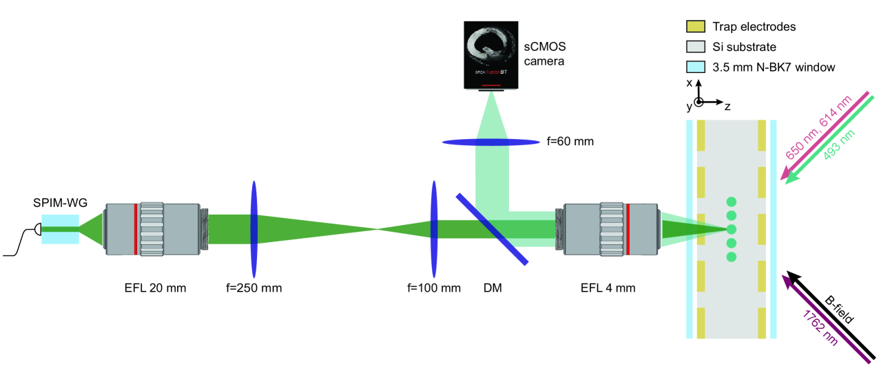
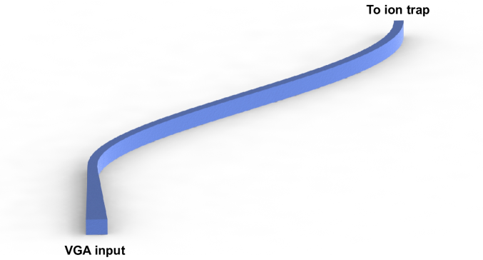
The VGA and SPIM-WG assembly is mounted on a stainless steel plate before integration with the rest of the optical system (see "Materials and methods"). This, combined with the fibre network used to interface between the laser source and the photonic chip as outlined in fig. 2, enables simple exchange of chips in the ion trap system with minimal realignment.
Cross-talk measurement using a single trapped ion
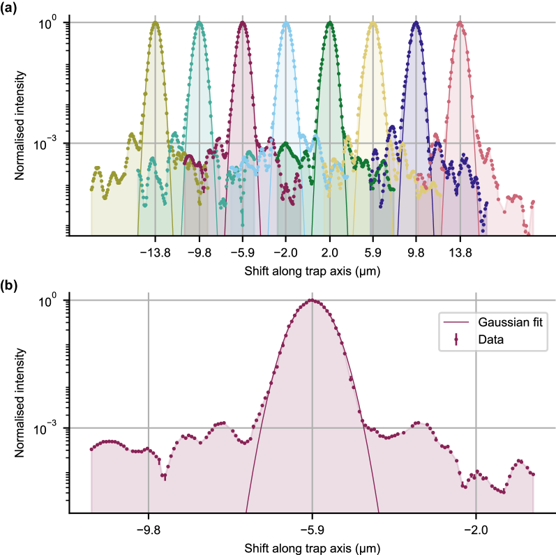
To characterise the performance of the fully integrated individual addressing setup, we measured the beams’ spatial profiles by using a single ion as a point-like sensor. When a single beam is directed at the ion, it introduces an AC Stark shift on the quadrupole transition frequencies between states in the and levels. This shift is proportional to the intensity of the light experienced by the ion. To characterise the spatial intensity distribution from the SPIM-WG output, we transported the ion from the trap centre to an axially displaced position (see fig. 7) and measured the quadrupole frequency shift as a function of . We were thus able to measure the beam profiles, the beam spacing, and the cross-talk of the system.
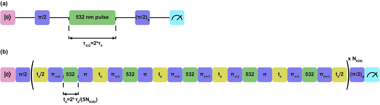
For the purpose of this measurement we used the transition as it exhibits the lowest magnetic field sensitivity of all available transitions for the magnetic field direction and the beam geometry shown in fig. 7. The frequency shift introduced by the beam can be seen as a rotation on the qubit state with the phase proportional to the magnitude of the AC Stark shift, and hence proportional to the beam intensity. To estimate this phase in a way that is robust to additive errors, such as those accumulated during state preparation and measurement, we used a robust phase estimation protocol[32, 33] (RPE). To enhance the system’s coherence time and hence increase the available probe duration (therefore also increasing the dynamic range of the measurement), we embedded the RPE sequence inside a Knill dynamical decoupling sequence[34] (KDD). Further details on the sequences used can be found in the "Materials and methods" section.
The results from this measurement are shown in fig. 8. We measured a mean beam waist radius of and a mean channel spacing of . For all channels, the cross-talk level was below , with a lowest measured cross-talk of . The variation in cross-talk across the chip was most likely due to light leakage through the fibre AOMs as well as aberrations and/or scatter from the optical components in the beam path that affect the channels non-uniformly.
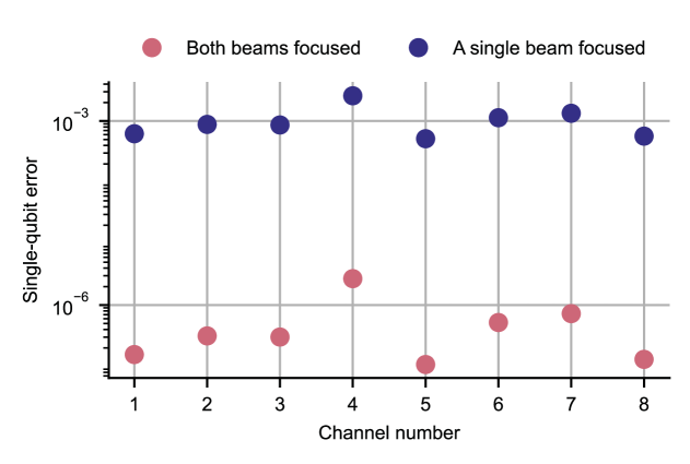
In fig. 9 we plot the error introduced to the state of a target ion’s nearest-neighbours for the data shown in fig. 8. We consider two cases: when a single beam is focused down on the target ion, and the case of a Raman transition where both beams are focused on the target ion. The former is relevant when the qubit transition is itself an optical transition, or when a two-photon Raman process is used and one of the beams is global for the entire qubit register. For each channel we sum the nearest-neighbour contributions (except for the edge channels where there is a single contribution). In both cases this error is much lower than, or comparable to, state-of-the-art two-qubit gate errors[3, 18, 5] and will therefore not limit the device performance. The cross-talk performance can be enhanced even further with well-known techniques such as coherent cancellation[35] or composite pulse sequences[36].
Discussions
We have presented a scalable and configurable way for individual optical addressing in chains of trapped atomic ions. We have designed and fabricated an SPIM-WG chip that offers a very high RI contrast between the core and the cladding, therefore achieving very low cross-talk at a small channel separation. The photonic chip is coupled with low loss to a fibre network that enables individual phase, frequency, and amplitude control of each of the channels, thus enabling parallel operations.
Measurements of the performance of our individual addressing system, optimised for light, using a single trapped ion showed cross-talk well below across the chip. The corresponding estimated worst-case nearest-neighbour error is if both beams are focused on a single ion or if one beam is focused on the ion and the second beam is global for the register. In the latter case, well-known techniques such as composite pulses or coherent cancellation can be used to further reduce this error.
The procedure used to manufacture the SPIM-WGs is highly flexible and so it can be used to create devices with a large number of channels, as well as devices with non-uniform channel spacing. The latter capability is important for applications in ion traps that do not have sufficient degrees of freedom to generate anharmonic potentials to keep the ion spacing uniform across the ion chain, or where harmonic potentials are desired. Preliminary results from the characterisation of devices with 32 channels show no degradation of performance in terms of cross-talk and minimal change in propagation losses. In addition, the same technique can be used to manufacture devices optimised for use at other optical wavelengths and therefore be integrated into setups using different ion species and/or different gate mechanisms.
In conclusion, we have presented a novel method to individually optically address chains of trapped atomic ions. Our method achieves significantly lower cross-talk compared to existing methods integrated with trapped-ion setups, while maintaining high scalability and flexibility.
Materials and methods
Mode progression in the SPIM-WG chip
SPIM-WG chip integration into the ion trap setup
To couple light from the VGA to the photonic chip, we kept the chip fixed and placed the VGA on a 6-axis positioning stage as shown in fig. 11. We imaged the chip output on a camera to evaluate the amount of light coupled from the VGA. We optimised the position of the VGA to maximise the average coupling efficiency, while simultaneously keeping the coupling efficiency across all channels as uniform as possible. Due to tolerances in the VGA spot size and spacing, the average coupling efficiency we achieved when optimising for all channels was lower than the maximum coupling efficiency that we could achieve for a single channel. In the devices used for the demonstration here, we achieved an average coupling efficiency of .
As outlined in the main text, the coupling between the VGA and the chip is extremely sensitive to relative position changes between the VGA and the chip. In addition to changes in the power in each channel, changes in the coupling efficiency can also modify the phase and/or polarisation of the light that lead to gate errors. To ensure the coupling between the VGA and the chip stays constant during system operation, after optimising the coupling between the two components, the VGA was glued to the chip using the NOA061 UV curing glue as shown in fig. 11(b). To avoid changes in the coupling while the glue was curing, we cured at a gradually increasing UV power over hours.
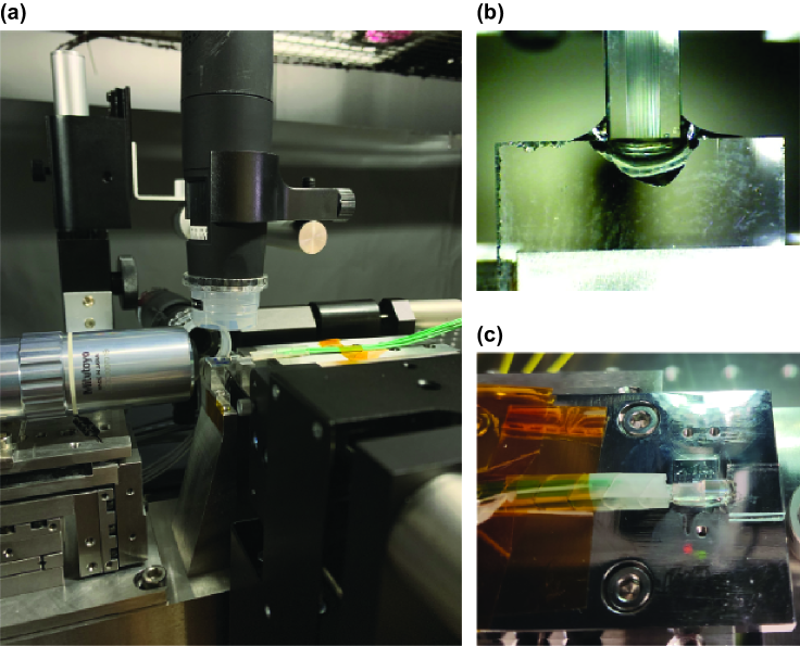
The VGA and photonic chip assembly was then glued to a stainless steel plate and was transported to the ion trap system. This stainless steel plate was then bolted on a positioning stage that is part of the setup as shown in fig. 11(c). Upon exchanging chips, the stainless steel plate with the glued VGA-photonic chip assembly is the only component that needs to be exchanged, while the remaining optical setup is left unchanged. Therefore only minimal realignment is necessary following chip exchange.
Robust phase estimation for an AC Stark shift measurement
We used the AC Stark shift induced by a single beam on the transition to measure the intensity of the beams and hence characterise the chip output at the ion position. This AC Stark shift introduces a relative phase between the two states that is proportional to the beam intensity. We used robust phase estimation [32, 33] (RPE) as shown in fig. 12(a) to estimate that phase. This significantly reduced our sensitivity to other systematic errors such as state preparation and measurement errors. To reduce the sensitivity of the system to decoherence and enable longer probing durations for the RPE sequence (hence also increasing the measurement dynamic range) we embedded the RPE sequence as part of a Knill dynamical decoupling sequence[34] (KDD) as shown in fig. 12(b). For probe durations shorter than the system coherence time, the RPE sequence was embedded in a spin-echo sequence instead. This avoided pulses with durations comparable to the AOM settling time constants. For probe durations longer than the system coherence time, the KDD sequence in fig. 12(b) was used and the number of KDD pulses was tuned to ensure that the maximum duration between consecutive -pulses did not exceed the system coherence time. In this experiment this duration was set to .
Acknowledgements
We thank A. Sinclair, G. Wilpers, and team at NPL for providing the ion trap and vacuum package used in this work. We thank Viviene Dela Cruz for contributing to the SPIM-WG characterisation. This work was supported by a UKRI FL Fellowship (MR/S03238X/1); the US Army Research Office (W911NF-20-1-0038); the UK EPSRC Hub in Quantum Computing and Simulation (EP/T001062/1); EPSRC Fellowship (EP/T00326X/1); Marie Curie Fellowship UKRI guarantee (EP/X024296/1); Austrian Science Fund (I3984-N36). C.H. acknowledges St. John’s College, Oxford for support through a Junior Research Fellowship. D.P.N. thanks Merton College, Oxford for the same. A.S.S. acknowledges funding from the JT Hamilton scholarship from Balliol College, Oxford.
Author contributions
B.S. designed and fabricated the SPIM-WG photonic chips. B.S. conducted various simulations and performed the classical tests of the chips. A.S.S. designed and implemented the systems and procedures used to integrate the chips with the ion trap apparatus. A.S.S. and D.P.N. took the single-ion measurements. A.S.S. performed the data analysis. M.W. and A.W. assisted with the photonic chip fabrication, characterization and waveguide mode analysis. C.H. analysed the polarisation and phase effects of the waveguide coupling errors, and assisted with microscopy. A.J. and S.M. performed the measurements and the analysis of the waveguide refractive index properties. A.S.S. and F.P. set up the ion trap experiment. J.D.L., A.V.B., and F.P. contributed to the experiment apparatus and supported the operation of the experiment. M.J.B.and C.J.B. obtained funding and supervised the project. A.S.S. and B.S. wrote the manuscript, with assistance from M.J.B and C.J.B. A.W. assisted with figure preparation. All authors reviewed the manuscript.
Conflict of interest
The authors declare no competing interests.
References
- [1] Cirac, J. I. & Zoller, P. Quantum Computations with Cold Trapped Ions. \JournalTitlePhysical Review Letters 74, 4091–4094 (1995).
- [2] Harty, T. et al. High-Fidelity Preparation, Gates, Memory, and Readout of a Trapped-Ion Quantum Bit. \JournalTitlePhysical Review Letters 113, 220501 (2014).
- [3] Ballance, C., Harty, T., Linke, N., Sepiol, M. & Lucas, D. High-Fidelity Quantum Logic Gates Using Trapped-Ion Hyperfine Qubits. \JournalTitlePhysical Review Letters 117, 060504 (2016).
- [4] Clark, C. R. et al. High-Fidelity Bell-State Preparation with Optical Qubits. \JournalTitlePhysical Review Letters 127, 130505 (2021).
- [5] Srinivas, R. et al. High-fidelity laser-free universal control of trapped ion qubits. \JournalTitleNature 597, 209–213 (2021).
- [6] Wang, P. et al. Single ion qubit with estimated coherence time exceeding one hour. \JournalTitleNature Communications 12, 233 (2021).
- [7] An, F. A. et al. High Fidelity State Preparation and Measurement of Ion Hyperfine Qubits with . \JournalTitlePhysical Review Letters 129, 130501 (2022).
- [8] Wineland, D. et al. Experimental issues in coherent quantum-state manipulation of trapped atomic ions. \JournalTitleJournal of Research of the National Institute of Standards and Technology 103, 259 (1998).
- [9] Nägerl, H., Bechter, W., Eschner, J., Schmidt-Kaler, F. & Blatt, R. Ion strings for quantum gates. \JournalTitleApplied Physics B 66, 603–608 (1998).
- [10] Leu, A. D. et al. Fast, high-fidelity addressed single-qubit gates using efficient composite pulse sequences (2023). ArXiv:2305.06725 [quant-ph].
- [11] Srinivas, R. et al. Coherent Control of Trapped-Ion Qubits with Localized Electric Fields. \JournalTitlePhysical Review Letters 131, 020601 (2023).
- [12] Leibfried, D. Individual addressing and state readout of trapped ions utilizing rf micromotion. \JournalTitlePhysical Review A 60, R3335–R3338 (1999).
- [13] Warring, U. et al. Individual-Ion Addressing with Microwave Field Gradients. \JournalTitlePhysical Review Letters 110, 173002 (2013).
- [14] Wang, S. X., Labaziewicz, J., Ge, Y., Shewmon, R. & Chuang, I. L. Individual addressing of ions using magnetic field gradients in a surface-electrode ion trap. \JournalTitleApplied Physics Letters 94, 094103 (2009).
- [15] Seck, C. M. et al. Single-ion addressing via trap potential modulation in global optical fields. \JournalTitleNew Journal of Physics 22, 053024 (2020).
- [16] Crain, S., Mount, E., Baek, S. & Kim, J. Individual addressing of trapped ion qubits using a microelectromechanical systems-based beam steering system. \JournalTitleApplied Physics Letters 105, 181115 (2014).
- [17] Shih, C.-Y. et al. Reprogrammable and high-precision holographic optical addressing of trapped ions for scalable quantum control. \JournalTitlenpj Quantum Information 7, 1–8 (2021).
- [18] Wang, Y. et al. High-Fidelity Two-Qubit Gates Using a Microelectromechanical-System-Based Beam Steering System for Individual Qubit Addressing. \JournalTitlePhysical Review Letters 125, 150505 (2020).
- [19] Pogorelov, I. et al. Compact Ion-Trap Quantum Computing Demonstrator. \JournalTitlePRX Quantum 2, 020343 (2021).
- [20] Egan, L. N. SCALING QUANTUM COMPUTERS WITH LONG CHAINS OF TRAPPED IONS. Ph.D. thesis, Unviersity of Maryland (2021).
- [21] Binai-Motlagh, A. et al. A guided light system for agile individual addressing of qubits with level intensity crosstalk (2023). ArXiv:2302.14711 [physics, physics:quant-ph].
- [22] Timpu, F. et al. Laser-Written Waveguide Array Optimized for Individual Control of Trapped Ion Qubits in a Chain. In 2022 European Conference on Optical Communication (ECOC), 1–4 (2022).
- [23] Wilpers, G., See, P., Gill, P. & Sinclair, A. G. A compact UHV package for microfabricated ion-trap arrays with direct electronic air-side access. \JournalTitleApplied Physics B 111, 21–28 (2013).
- [24] Choonee, K., Wilpers, G. & Sinclair, A. G. Silicon microfabricated linear segmented ion traps for quantum technologies. In 2017 19th International Conference on Solid-State Sensors, Actuators and Microsystems (TRANSDUCERS), 615–618 (2017).
- [25] Sun, B. et al. On-chip beam rotators, adiabatic mode converters, and waveplates through low-loss waveguides with variable cross-sections. \JournalTitleLight: Science & Applications 11, 214 (2022).
- [26] Cetina, M. et al. Control of Transverse Motion for Quantum Gates on Individually Addressed Atomic Qubits. \JournalTitlePRX Quantum 3, 010334 (2022).
- [27] West, A. D., Putnam, R., Campbell, W. C. & Hamilton, P. Tunable transverse spin–motion coupling for quantum information processing. \JournalTitleQuantum Science and Technology 6, 024003 (2021).
- [28] Sun, B. et al. High Speed Precise Refractive Index Modification for Photonic Chips through Phase Aberrated Pulsed Lasers (2023). ArXiv:2307.14451 [physics].
- [29] Snyder, A. W. & Love, J. D. Optical Waveguide Theory (Boston, MA, 1984).
- [30] Lin, G.-D. et al. Large-scale quantum computation in an anharmonic linear ion trap. \JournalTitleEurophysics Letters 86, 60004 (2009).
- [31] Zhang, Z. et al. Branching fractions for decays in . \JournalTitlePhysical Review A 101, 062515 (2020).
- [32] Kimmel, S., Low, G. H. & Yoder, T. J. Robust calibration of a universal single-qubit gate set via robust phase estimation. \JournalTitlePhysical Review A 92, 062315 (2015).
- [33] Rudinger, K., Kimmel, S., Lobser, D. & Maunz, P. Experimental Demonstration of a Cheap and Accurate Phase Estimation. \JournalTitlePhysical Review Letters 118, 190502 (2017).
- [34] Souza, A. M., Álvarez, G. A. & Suter, D. Robust Dynamical Decoupling for Quantum Computing and Quantum Memory. \JournalTitlePhysical Review Letters 106, 240501 (2011).
- [35] Flannery, J. et al. Optical Crosstalk Mitigation for Individual Addressing in a Cryogenic Ion Trap. In 2022 IEEE International Conference on Quantum Computing and Engineering (QCE), 816–817 (2022).
- [36] Brown, K. R., Harrow, A. W. & Chuang, I. L. Arbitrarily accurate composite pulse sequences. \JournalTitlePhysical Review A 70, 052318 (2004).