2. National Institute of Standards and Technology, Boulder, CO 80305, USA
3. Quantum Optoelectronics Laboratory, School of Physical Science and Technology, Southwest Jiaotong University, Chengdu, 610031, China
11email: : yiwenwang.nju@gmail.com, lfwei@swjtu.edu.cn
Measurement of optical constants of TiN and TiN/Ti/TiN multilayer films for microwave kinetic inductance photon-number-resolving detectors
Abstract
We deposit thin titanium-nitride (TiN) and TiN/Ti/TiN multilayer films on sapphire substrates and measure the reflectance and transmittance in the wavelength range from nm to nm using a spectrophotometer. The optical constants (complex refractive indices), including the refractive index and the extinction coefficient , have been derived. With the extracted refractive indices, we propose an optical stack structure using low-loss amorphous Si (a-Si) anti-reflective coating and a backside aluminum (Al) reflecting mirror, which can in theory achieve 100% photon absorption at nm. The proposed optical design shows great promise in enhancing the optical efficiency of TiN-based microwave kinetic inductance photon-number-resolving detectors.
Keywords:
optical constants, refractive index, TiN, microwave kinetic inductance detectors1 Introduction
Photon-number-resolving (PNR) detectors are able to directly measure the photon number and energy in a pulse of incident light. In particular, the PNR detectors at visible and near-infrared wavelengths have important applications in many fields such as quantum secure communications hiskett2006long , linear optics quantum computing knill2001scheme , quantum optics experiments Bell2013 and optical quantum metrology zwinkels2010photometry . To meet the requirements of these applications, an ideal PNR detector should have both high energy resolution and high system detection efficiency. By minimizing the fiber-to-detector coupling losses and using optical stack structures that enhance the photon absorption by the absorber material, transition edge sensors (TESs) have demonstrated high energy resolution and near unity system detection efficiency at near-infrared wavelengths miller2003demonstration ; lita2008counting ; Lita10 ; calkins2013high ; lolli2012ti ; brida2012quantum ; lolli2013high .
Another type of superconducting detector with intrinsic photon-number-resolving and energy-resolving capability is the microwave kinetic inductance detector (MKID) Day2003 . As compared to TESs, MKIDs are easy to fabricate and multiplex into large arrays. Single-photon counting at telecommunication wavelengths (near-infrared) with titanium-nitride (TiN) MKIDs was first demonstrated in reference JG12 . Recently, by optimizing the MKID design, we have achieved an energy resolution of eV and resolved up to photons per optical pulse at nm using MKIDs made from TiN/Ti/TiN trilayer films WG17 . Although the energy resolution of these detectors is already impressive, little effort has been made to improve their optical efficiency.
The major sources that limit the optical efficiency of MKIDs include fiber-to-detector coupling efficiency, photon loss due to reflection from and transmission through the thin TiN layer. As the first step to improve the optical efficiency of photon-number-resolving TiN-MKIDs, in this paper, we show measurements of the optical constants (complex refractive indices) for thin TiN and TiN/Ti/TiN multilayer films. We then propose an optical stack structure that can in theory achieve 100% photon absorption at nm for TiN-based MKIDs.
2 Principle
In this section, we briefly introduce the optical transfer matrix theory which is commonly used to obtain the reflectance and transmittance Nestell72 for a multilayer optical structure.
Consider a beam of light from the air is normally incident onto an optical stack consisting of layers and exit into the air. Assume the refractive index of air is and each layer has thickness of and complex refractive index of (here and are wavelength dependent refractive index and extinction coefficient for the -th layer, = 1, …, K), the magnitude of the incident electromagnetic wave and the transmitted wave are related by the products of the transfer matrices as
| (9) |
where is called the characteristic matrix of dielectric films and is defined as the optical admittance. It follows from Eq. (1) that the reflectance and transmittance of the whole optical stack are given by
| (10) | |||||
| (11) |
Eq. (2-3) allow us to solve for the and values of a layer in the optical stack from the combined measurements of the reflectance and transmittance , if we know the complex refractive indices for all the other layers and the thickness of all the layers. In Section , we use this method to extract the complex refractive indices for thin TiN and TiN/Ti/TiN multilayer films deposited on thick sapphire substrates. On the other hand, when the complex refractive indices and thickness of each layer are given, Eq. (2-3) also allow us to directly calculate the wavelength dependent and of the multilayer stack, which is used in Section to design the optimized optical structure that can maximize the photon absorption at nm.
3 Measurements of optical constants
We deposited thin stoichiometric TiN and TiN/Ti/TiN multilayer films on m thick double-side polished sapphire substrates. The multilayer film comprises a stack of 7 layers with TiN at the top and bottom interface and alternating layers of Ti and TiN in the middle. The detailed deposition conditions and processes can be found in reference Vissers10 ; Vissers2013 . To precisely determine the optical constants of these thin films, one should properly choose the film thickness. On one hand, if the film is too thin, the uncertainty in the film thickness will result in large errors in the derived and values. On the other hand, if the film is too thick, the transmitted light will be too weak to be measured accurately due to instrument noise and background stray light. We have chosen a target thickness of 60 nm for both films. The actual thicknesses were carefully measured by a profilometer which reports nm for the stoichiometric TiN film and nm for the TiN/Ti/TiN multilayer.
The reflectance and transmittance in the wavelength range from nm to nm were measured at room temperature using a commercial spectrophotometer (PerkinElmer’s LAMBDA 1050), and the results are shown in Fig. 1(a) and (b), respectively. From the and data, it is straightforward to obtain the absorption as , which is of practical interest since it directly affects the optical efficiency.
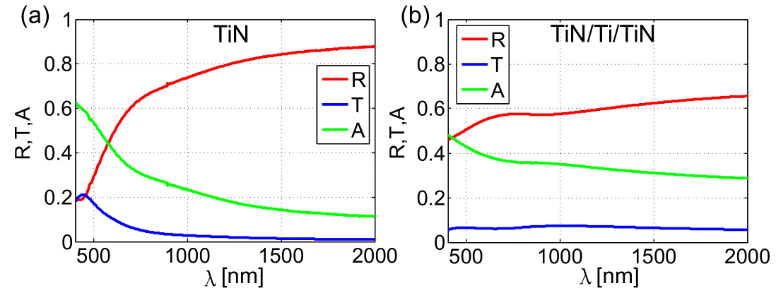
We also measured the and data for a m thick double-side polished bare sapphire wafer, which can be easily analyzed with the transfer matrix theory introduced in Section 2 to give the complex refractive index of sapphire ( and ), which is approximately wavelength independent. We find the measured optical constants of sapphire match well with the tabulated values sapphire . For the two-layer stack of TiN film on sapphire substrate, we have the measured thickness of the TiN layer ( nm for stoichiometric TiN and nm for TiN/Ti/TiN multilayer), the vendor specified wafer thickness (m) and the derived complex refractive index ( and ) of the sapphire substrate. Then Eq. (2-3) reduce to two nonlinear equations with two unknown variables ( and of the TiN layer),
| (14) |
where and are the measured reflectance and transmittance data. The above equations can be solved numerically Nestell72 at a specific wavelength . Note that we take the thick-substrate approximation rosenberg2004near that assumes reflections off the back surface add incoherently, so that we can get smooth and vs. wavelength curve.
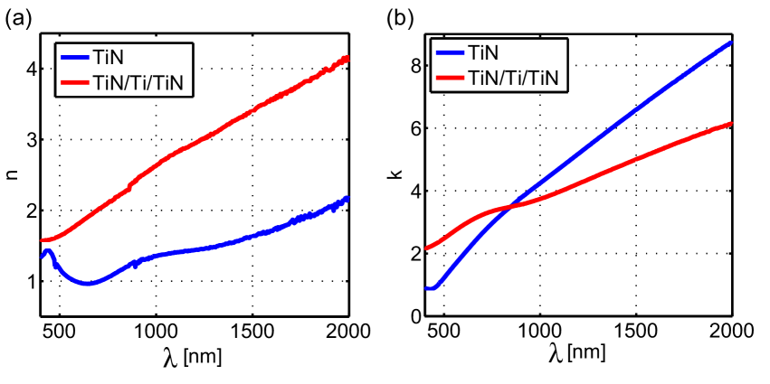
Fig. 2(a) and (b) plot the derived refractive index and extinction coefficient as a function of wavelength. For stoichiometric TiN film, one can see a low refractive index in the visible wavelength and even at the wavelength range from nm to nm, which is similar to previous optical measurements on TiN films Valkonen86 ; karlsson1982optical . The for TiN/Ti/TiN multilayer is higher and increases monotonically with wavelength, which resembles the properties of pure Ti film. ranges from to is also a signature of pure Ti film sapphire .
4 Optical designs for enhancement of photon absorption
In this Section, we use the and values derived in the previous section to design optimal stack structures that can enhance the photon absorption efficiency at a particular wavelength. In the following we mainly discuss the designs for TiN/Ti/TiN multilayers at nm, because photon-number-resolving MKIDs based on TiN/Ti/TiN multilayer films have already demonstrated high energy resolution and good multiphoton discrimination capability at nm WG17 , and also because the TiN/Ti/TiN multilayer has superior uniformity (as compared to substoichiometric TiN films) which is critical for scaling into large MKID arrays.
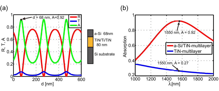
We present two optical designs for enhancing photon absorption in TiN/Ti/TiN multilayer films. The first relative simple structure includes a single amorphous Si (a-Si) anti-reflective (AR) coating layer deposited on top of a nm thick TiN/Ti/TiN multilayer film. We choose a-Si because it has shown reduced two-level systems (TLSs) and low microwave loss comparing to other dielectric materials, such as SiO2 and Si3N4 martinis2005decoherence . We choose a relative thick ( nm) TiN/Ti/TiN multilayer film to enhance the absorption in the film and prevent light from penetrating the film. Using the extracted values of and , we calculate expected performance of this structure in terms of reflectance, transmittance and absorption at nm wavelength as a function of the thickness of a-Si AR coating. As shown in Fig. 3(a), the absorption varies periodically with the thickness of Si layer and a maximum absorption of is first reached at a coating thickness of nm, which suggests an optimal design illustrated by the cartoon in Fig. 3(a). Fig. 3(b) shows the simulated absorption of this optimal stack (red curve) between nm to nm, which is compared to the TiN/Ti/TiN multilayer film alone without AR coating (blue curve). It is clear that the AR coating design has significantly enhanced the absorption, from less than 30% to over 90% around nm.
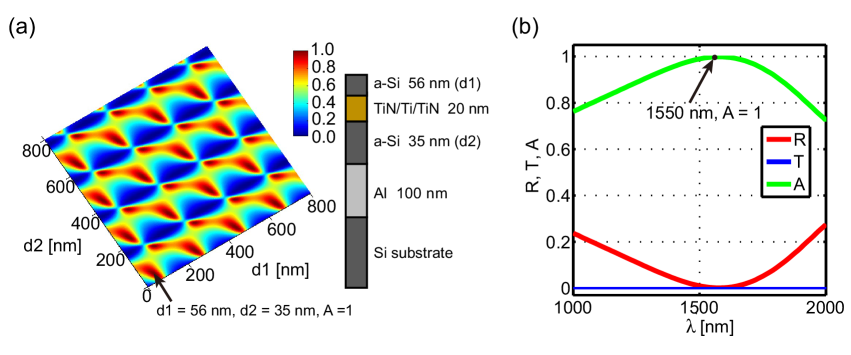
While the single-layer a-Si AR coating solution is attractive and relative easy to implement (and we plan to test it in the future), the theoretical maximum absorption is still less than unity, so we further propose another optical stack design that can achieve 100% absorption at 1550nm. In this design, a thin TiN/Ti/TiN trilayer film is sandwiched between two a-Si layers of different thicknesses and a thick aluminum (Al) layer is buried under the sandwich. Different from the first design, the second design accommodates a thin nm TiN/Ti/TiN trilayer film, which is the film used in our previous photon-counting experiment WG17 . In that experiment, we found that absorbers with smaller volume showed larger responsivity and better energy resolution. We use an Al layer as a bottom mirror to create an optical cavity and embed the thin TiN/Ti/TiN trilayer film in the cavity to enhance the absorption. An important reason for choosing Al (instead of Au as used in optical TES) as the mirror material is that Al is superconducting which is expected not to introduce metal losses and degrade the quality factor of the MKIDs.
Fig. 4(a) shows the simulated absorption at nm in the two-dimensional parameter space of the two a-Si layer thicknesses ( and ). The absorption varies periodically with and and a maximum absorption of unity is first reached at nm and nm. The stack structure with optimal layer thicknesses is illustrated by the cartoon on the right of Fig. 4(a). In Fig. 4(b), we plot the wavelength-dependent absorption of this optimal stack structure, which shows that 100% absorption and 0% reflectance have been achieved at the wavelength of nm.
5 Conclusion
We have successfully determined the optical constants (refractive index and extinction coefficient ) of superconducting stoichiometric TiN and TiN/Ti/TiN multilayer thin films, from combined measurements of reflectance and transmittance at the wavelength ranging from nm to nm. By utilizing the extracted and values, two optical stack designs have been presented and discussed, which may significantly improve photon absorption into TiN/Ti/TiN multilayer films. In particular, by embedding the TiN/Ti/TiN film in an optical cavity structure one may in theory achieve unity absorption at nm. The proposed designs show great promise in achieving high system detection efficiency in near-infrared photon-number-resolving TiN MKIDs.
Acknowledgements.
The TiN films were deposited in the NIST-Boulder micro-fabrication facility. We thank Dr. Adriana. E. Lita for useful discussions. This work was supported in part by the National Natural Science Foundation of China (Grant Nos. 61301031, U1330201).References
- (1) P. A. Hiskett, D. Rosenberg, C. G. Peterson, R. J. Hughes, S. Nam, A. Lita, A. Miller, and J. Nordholt. New Journal of Physics 8, 9, 193 (2006).
- (2) E. Knill, R. Laflamme, and G. J. Milburn. nature 409, 6816, 46–52 (2001).
- (3) M. Giustina, A. Mech, S. Ramelow, B. Wittmann, J. Kofler, J. Beyer, A. Lita, B. Calkins, T. Gerrits, S. W. Nam, et al. Nature 497, 7448, 227–230 (2013).
- (4) J. C. Zwinkels, E. Ikonen, N. P. Fox, G. Ulm, and M. L. Rastello. Metrologia 47, 5, R15 (2010).
- (5) A. J. Miller, S. W. Nam, J. M. Martinis, and A. V. Sergienko. Applied Physics Letters 83, 4, 791–793 (2003).
- (6) A. E. Lita, A. J. Miller, and S. W. Nam. Optics express 16, 5, 3032–3040 (2008).
- (7) A. E. Lita, B. Calkins, L. A. Pellouchoud, A. J. Miller, and S. Nam. Proc.SPIE 7681, 7681 – 7681 – 10 (2010). doi:10.1117/12.852221.
- (8) B. Calkins, P. L. Mennea, A. E. Lita, B. J. Metcalf, W. S. Kolthammer, A. Lamas-Linares, J. B. Spring, P. C. Humphreys, R. P. Mirin, J. C. Gates, et al. Optics express 21, 19, 22657–22670 (2013).
- (9) L. Lolli, E. Taralli, and M. Rajteri. Journal of Low Temperature Physics 167, 5-6, 803–808 (2012).
- (10) G. Brida, L. Ciavarella, I. P. Degiovanni, M. Genovese, L. Lolli, M. G. Mingolla, F. Piacentini, M. Rajteri, E. Taralli, and M. G. Paris. New Journal of Physics 14, 8, 085001 (2012).
- (11) L. Lolli, E. Taralli, C. Portesi, E. Monticone, and M. Rajteri. Applied Physics Letters 103, 4, 041107 (2013).
- (12) P. K. Day, H. G. LeDuc, B. A. Mazin, A. Vayonakis, and J. Zmuidzinas. Nature 425, 6960, 817–821 (2003).
- (13) J. Gao, M. R. Vissers, M. O. Sandberg, F. C. S. da Silva, S. W. Nam, D. P. Pappas, D. S. Wisbey, E. C. Langman, S. R. Meeker, B. A. Mazin, H. G. Leduc, J. Zmuidzinas, and K. D. Irwin. Applied Physics Letters 101, 14, 142602 (2012). doi:10.1063/1.4756916.
- (14) W. Guo, X. Liu, Y. Wang, Q. Wei, L. F. Wei, J. Hubmayr, J. Fowler, J. Ullom, L. Vale, M. R. Vissers, and J. Gao. Applied Physics Letters 110, 21, 212601 (2017). doi:10.1063/1.4984134.
- (15) J. E. Nestell and R. W. Christy. Appl. Opt. 11, 3, 643–651 (1972). doi:10.1364/AO.11.000643.
- (16) M. R. Vissers, J. Gao, D. S. Wisbey, D. A. Hite, C. C. Tsuei, A. D. Corcoles, M. Steffen, and D. P. Pappas. Applied Physics Letters 97, 23, 232509 (2010). doi:10.1063/1.3517252.
- (17) M. R. Vissers, J. Gao, M. Sandberg, S. M. Duff, D. S. Wisbey, K. D. Irwin, and D. P. Pappas. Applied Physics Letters 102, 23, 232603 (2013). doi:10.1063/1.4804286.
- (18) https://www.filmetrics.com/refractive-index-database.
- (19) D. Rosenberg, S. Nam, A. Miller, A. Salminen, E. Grossman, R. Schwall, and J. Martinis. Nuclear Instruments and Methods in Physics Research Section A: Accelerators, Spectrometers, Detectors and Associated Equipment 520, 1, 537–540 (2004).
- (20) E. Valkonen, C.-G. Ribbing, and J.-E. Sundgren. Appl. Opt. 25, 20, 3624–3630 (1986). doi:10.1364/AO.25.003624.
- (21) B. Karlsson, J.-E. Sundgren, and B.-O. Johansson. Thin Solid Films 87, 2, 181–187 (1982).
- (22) J. M. Martinis, K. B. Cooper, R. McDermott, M. Steffen, M. Ansmann, K. Osborn, K. Cicak, S. Oh, D. P. Pappas, R. W. Simmonds, et al. Physical Review Letters 95, 21, 210503 (2005).