Multi-Voltage and Level-Shifter Assignment Driven Floorplanning
Abstract— As technology scales, low power design has become a significant requirement for SOC designers. Among the existing techniques, Multiple-Supply Voltage (MSV) is a popular and effective method to reduce both dynamic and static power. Besides, level shifters consume area and delay, and should be considered during floorplanning. In this paper, we present a new floorplanning system, called MVLSAF, to solve multi-voltage and level shifter assignment problem. We use a convex cost network flow algorithm to assign arbitrary number of legal working voltages and a minimum cost flow algorithm to handle level-shifter assignment. The experimental results show MVLSAF is effective.
Index Terms—Voltage-Island, Multi-Voltage Assignment, Level Shifter Assignment, Floorplanning
I INTRODUCTION
As technology scales, low power design has become a significant requirement for system-on-chip designers. Many techniques were introduced to deal with power optimization. Among the existing techniques, Multiple-Supply Voltage (MSV) is one of the most effective methods for both dynamic and static power reduction while maintaining performance. In the MSV design, one of the most important problem is voltage assignment: timing critical modules are assigned to higher voltage while noncritical modules are assigned to lower voltage, so the power can be saved without degrading the overall circuit performance.
There are a number of previous works addressing voltage assignment in floorplanning. Among these works, voltage assignment is considered at various stages, including pre-floorplanning[4, 5]; during floorplanning[6, 7, 8, 9]; and post-floorplaning[10, 11, 12].
Level-shifter [1] has to be inserted to an interconnect when a lower voltage module drives a higher voltage module or a circuit may suffer from excessive short-circuit current energy. From [5, 9] we can observe that the number and the area of level shifters can not be ignored when modules increase. As a result, level-shifters may cause performance and area overhead, and should be considered during floorplanning. Accordingly, MSV aware floorplanning includes two major problems: voltage assignment and level shifter assignment, which make the design process much more complicated.
Lee et al.[5] handle voltage assignment by dynamic programming, and level shifters are inserted as soft blocks. An approach based on ILP is used in [11] for voltage assignment at the post-floorplanning stage. To make use of physical information among modules during floorplanning, Ma et al.[8] transform voltage assignment problem into a convex cost network flow problem. However, their approach consider neither level-shifters’ area overhead nor level-shifters’ physical infomation.
Yu et al.[9] use a convex cost network flow algorithm to assign voltage and a minimum cost flow algorithm to handle level-shifter assignment which considers level-shifters’ positions and areas. However, their work can only assign two legal working voltages. Besides, level shifters are assumed to be soft modules and ratios can not controlled well.
In this paper, we propose a new floorplanning system MVLSAF, which is extended from [9]. At floorplanning phase, we use: a convex cost network flow algorithm to assign multi-voltages; a minimum cost flow algorithm with more accurate model to assign level shifters.
The remainder of this paper is organized as follows. Section 2 defines the voltage-island driven floorplanning problem. Section 3 presents our algorithm flow. Section 4 reports our experimental results. At last, Section 5 concludes this paper.
.
II PROBLEM FORMULATION
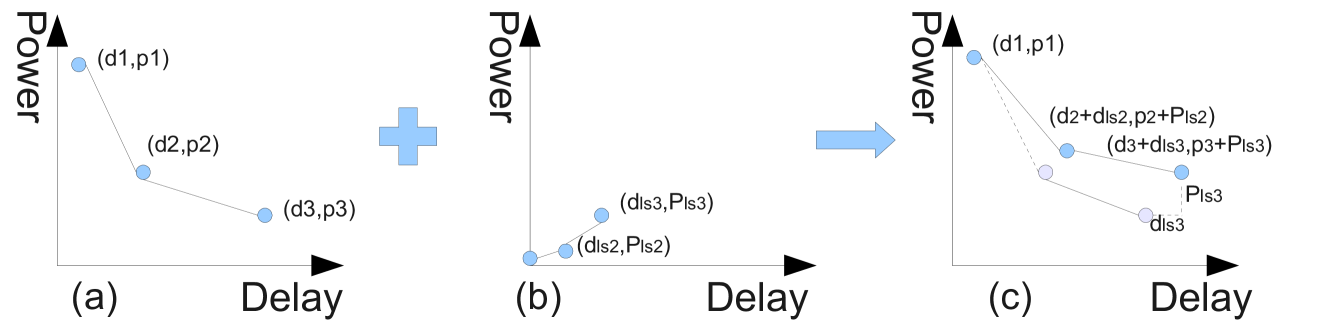
Definition 1 (DP-Curve).
The power-delay tradeoff of each module is represented by a DP-Curve , where each pair is the corresponding delay and power consumption when module is operated at voltage (Fig.1(a)).
We assume that power is a convex function of delay when each point is connected to its neighboring point(s) by a linear segment in the DP Curve. Besides, each level shifter has its own DP-Curve ( is delay and power consumption when it is driving voltage ). Lower voltage module needs bigger level shifter to drive other modules. Since bigger level shifter consumes more delay and power, we assume the level shifter’s DP-Curve is also convex(as shown if Fig.1(b)). We extend the problem in [9] to Multi-Voltage and Level-Shifter Assignment driven Floorplanning (MVLSAF):
Problem 1.
(MVLSAF) We are given following input to generate floorplanning result: minimize the area, power cost and wirelength; satisfying timing constraint; insert all the level-shifters in need.
| 1) | A set of modules, each module has its DP–curve. |
|---|---|
| 2) | A netlist and timing constraint . |
| 3) | Level-shifter’s area, ratio and DP-Curve. |
| 4) | Number of legal working voltage . |
III ALGORITHM of MVLSAF
Our work is similar to that presented in [9], in which a two phases framework is presented to deal with voltages and level-shifters assignment during floorplanning. However, our approach differs from [9] in the following ways: during voltage assignment, we support arbitrary number of legal voltages allowing further power reductions in certain applications; during level-shifter assignment, we adopt more accurate model to calculate possible level-shifter number in white space, which control level shifter under certain H/W ratio.
A Multi-Voltages Assignment
To take consumption of level-shifter into consider, for each module, we modify its DP-Curve: replace each pair by , where islevel shifter’s delay and power consumption. Modified DP-Curve is shown in Fig.1(c).
LEMMA 1.
is convex , .
LEMMA 2.
If and are convex, then is also convex.
THEOREM 1.
Modified DP-Curve is piecewise linear convex function with integer breakpoints, and we can apply convex cost flow algorithm to solve voltage assignment problem[3].
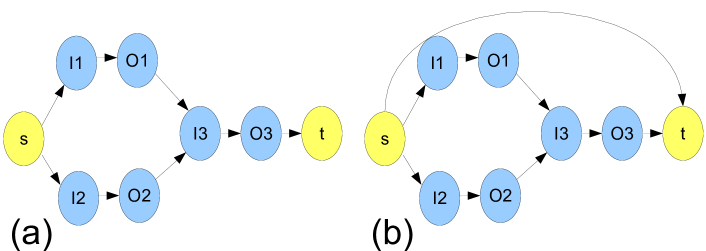
Given netlist , we translate it into (adding start node and end node , dividing each node into 2 nodes and , as shown in Fig.2(a)). So . And is connected to by a directed edge. We denote these new created edges as , denote edges as , and other edges as , and .
We can incorporate constraints and by transforming into , and define , s.t. . Accordingly, , and the transformed DAG is shown in Fig.2(b). Besides, we dualize the constraints using a nonnegative Lagrangian multiplier vector , obtaining the following Lagrangian subproblem:
| (2) |
We define function for each as follows:
| (3) |
THEOREM 2.
The function is a piecewise linear concave function of , and , is described in the following manner:
| (9) |
where .
To transform the problem into a minimum cost flow problem, we construct an expanded network . There are three kinds of edges to consider:
-
•
in E1:we introduce edges in , and the costs of these edges are: ; upper capacities: , where is a huge confficient; lower capacities are both 0.
-
•
in E2: cost, lower and upper capacity is , 0, M.
-
•
Edge in E3: two edges are introduced in , one with cost, lower and upper capacity as (), another is ().
Using the cost-scaling algorithm, we can solve the minimum cost flow problem in . For the residual network and solve a shortest path problem to determine shortest path distance from node to every other node. By implying that and for each , we can finally solve voltage assignment problem.
B Level-shifters Assignment
: Notation used in LS Assignment
| Room containing module | |
|---|---|
| Set of rooms, | |
| Set of LSs, | |
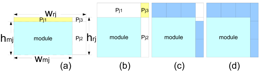
| Three parts of white spaces in . |
After voltage assignment, each module is assigned a voltage, then the number of level shifters is determined. In level shifter assignment we carry out minimum cost flow algorithm to try to assign every level-shifters one room. Compared with [9], we present a more accurate model estimating possible number of level shifters in white space to avoid too much ratio.
We construct a network graph , and then use a min-cost max-flow algorithm to determine which room each level shifter belong to.
-
•
.
-
•
.
-
•
Capacities: .
-
•
Cost: .
where and can refer to [9].
The algorithm of , which accurately estimates number of possible level shifters in white space, is shown in Algorithm 1. In room , white space is split into at most three parts: (as shown in Fig.3).
It can be shown that any flow in the network assigns level shifters to white spaces. The minimum cost flow algorithm can be run in polynomial time[3].
After level-shifter assignment, level shifters that can not be assigned to any room are belong to set . We use heuristic method to assign level shifters in , so more level shifters in , more ILO(Interconnect Length Overhead[9]). If white space is too narrow, then level shifters being assigned to are all belong to . More accurate model we used (Algorithm 1) can reduce the number of level shifters in and then reduces ILO.
IV EXPERIMENTAL RESULTS
: The Comparison Between the VLSAF and the Previous Work [9]
| Data | Power Cost | Wire Length w. LS | LS Number | ILO(%) | White Space(%) | Run Time(s) | ||||||
| [9] | MVLSAF | [9] | MVLSAF | [9] | MVLSAF | [9] | MVLSAF | [9] | MVLSAF | [9] | MVLSAF | |
| n10 | 189142 | 162794 | 15504 | 16474 | 9 | 11 | 0.37 | 0.12 | 10.96 | 11.54 | 3.36 | 3.96 |
| n30 | 146483 | 138463 | 43265 | 45388 | 25 | 42 | 0.07 | 0.21 | 14.28 | 17.63 | 21.0 | 19.83 |
| n50 | 143596 | 133564 | 94622 | 93296 | 114 | 151 | 0.28 | 0.50 | 22.63 | 22.95 | 41.37 | 49.35 |
| n100 | 135607 | 120885 | 185382 | 181280 | 153 | 167 | 0.49 | 0.34 | 27.05 | 26.07 | 436.65 | 414.7 |
| n200 | 129615 | 117538 | 349562 | 344111 | 203 | 248 | 0.44 | 0.46 | 36.35 | 34.84 | 1980.4 | 2036.4 |
| n300 | 216554 | 206354 | 552616 | 568364 | 366 | 417 | 0.49 | 0.53 | 37.73 | 38.54 | 2384.3 | 2377.2 |
| Avg | 160166 | 146599 | 206825 | 208152 | 145 | 172 | 0.36 | 0.36 | 24.83 | 25.26 | 811.2 | 816.8 |
| Diff | - | -8.5% | - | +0.6% | - | +18.6% | - | 0% | - | +1.7% | - | +0.7% |
: Experimental Results with More Legal Working Voltage
| Data |
|
|
|
|
|
|
Data |
|
|
|
|
|
|
||||||||||||||||||||||||||
|---|---|---|---|---|---|---|---|---|---|---|---|---|---|---|---|---|---|---|---|---|---|---|---|---|---|---|---|---|---|---|---|---|---|---|---|---|---|---|---|
| n10 | 2 | 189142 | 15341 | 9 | 0.10 | 10.21 | 3.05 | n100 | 2 | 133775 | 178685 | 122 | 0.17 | 26.45 | 431.7 | ||||||||||||||||||||||||
| 3 | 163352 | 16386 | 10 | 0.13 | 11.58 | 3.03 | 3 | 131394 | 180023 | 150 | 0.50 | 26.8 | 438.05 | ||||||||||||||||||||||||||
| 4 | 162794 | 16474 | 11 | 0.12 | 11.54 | 3.96 | 4 | 120885 | 181280 | 167 | 0.34 | 26.07 | 414.7 | ||||||||||||||||||||||||||
| n30 | 2 | 146483 | 42591 | 25 | 0.1 | 15.0 | 21.5 | n200 | 2 | 127044 | 344010 | 204 | 0.42 | 35.64 | 1955.8 | ||||||||||||||||||||||||
| 3 | 139466 | 45103 | 42 | 0.32 | 15.85 | 20.82 | 3 | 112801 | 331627 | 242 | 0.55 | 35.44 | 1949.4 | ||||||||||||||||||||||||||
| 4 | 138463 | 45388 | 42 | 0.21 | 17.63 | 19.83 | 4 | 117538 | 344111 | 248 | 0.46 | 34.84 | 2036.4 | ||||||||||||||||||||||||||
| n50 | 2 | 144489 | 93459 | 104 | 0.25 | 22.05 | 49.21 | n300 | 2 | 223574 | 548502 | 321 | 0.23 | 37.88 | 2363.9 | ||||||||||||||||||||||||
| 3 | 132199 | 94105 | 130 | 0.37 | 22.72 | 51.10 | 3 | 218636 | 556718 | 389 | 0.44 | 37.14 | 2390.2 | ||||||||||||||||||||||||||
| 4 | 133564 | 93296 | 151 | 0.50 | 22.95 | 49.35 | 4 | 206354 | 568364 | 417 | 0.53 | 38.54 | 2377.2 |
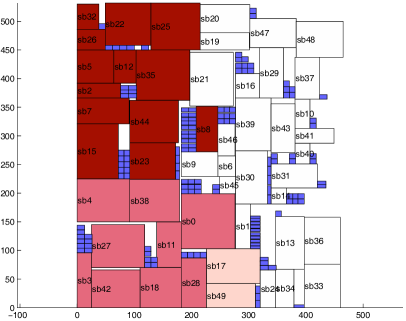
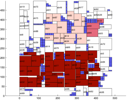
We implemented algorithm MVLSAF in the C++ programming language and executed on a Linux machine with a 3.0GHz CPU and 1GB Memory. Fig. 4 shows the experimental results of the benchmarks n50 and n100.
We use CBL[2] to represent every floorplan generated. Besides, all the multi-pin nets are decomposed into a set of source-sink two-pin nets. Cost function in floorplanning is: , where and represent the floorplan area and wire length; represents the total power consumption; represents the power network resource; and records the number of level shifters that can not be assigned.
The previous work [9] is the recent one in handling floorplanning problem considering voltage and level-shifter assignment. We performed our algorithm MVLSAF and VLSAF in [9] on the same test circuits, which are based on the GSRC benchmarks adding power and delay specifications. For each test circuit, we set as 4, and run MVLSAF and VLSAF 5 times. Table II lists the average results. The column Power Cost means the actual power consumption. When allowing four legal working voltages, MVLSAF can save 8.5% power while not deteriorating wirelength, dead space and run time. The column ILO and the column LS Number show that using more accurate model in level shifter assignment, even level shifters number increases 18.6% ILO does not increase.
In order to demonstrate the effectiveness of our approach, we have done three sets of experiments in which the number of legal working voltage for each module is set two, three and four. The detailed results are listed in Table III.
V CONCLUSIONS
We have extended framework in [9] to solve multi-voltage and level shifter assignment problem: a convex cost network flow algorithm to assign arbitrary number of legal working voltages; a minimum cost flow algorithm to handle level shifter assignment. Experimental results have shown that our framework is effective in reducing power cost while considering level shifters’ positions and areas.
References
- [1] David Lackey, Paul Zuchowski and J. Cohn. Managing power and performance for system-on- chip designs using voltage islands. ICCAD, pages 195–202, 2002.
- [2] Xianlong Hong, Sheqin Dong. Non-slicing floorplan and placement using corner block list topological representation. IEEE Transaction on CAS, 51:228–233, 2004.
- [3] R.K. Ahuja, D.S. Hochbaum, and J.B. Orlin Solving the convex cost integer dual network flow problem. Management Science, 49(7):950-964, 2003
- [4] W.L.Hung, G.M.Link and J.Conner. Temperature-aware voltage islands architecting in system-on-chip design. ICCD, 2005.
- [5] W.P.Lee and Y.W.Chang. Voltage island aware floorplanning for power and timing optimization. ICCAD, pages 389–394, 2006.
- [6] Q.Ma and F.Y.Young. Voltage Island-Driven Floorplanning. ICCAD, pages 644–649, 2007.
- [7] D.Sengupta and R.Saleh. Application-driven Floorplan-Aware Voltage Island Design. DAC, pages 155–160, 2008.
- [8] Q.Ma and F.Y.Young. Network flow-based power optimization under timing constraints in MVS-driven floorplanning. ICCAD, 2008.
- [9] Bei Yu, Sheqin Dong, Satoshi GOTO and Song Chen. Voltage-Island Driven Floorplanning Considering Level-Shifter Positions. GLSVLSI, 2009.
- [10] W.K.Mak and J.W.Chen. Voltage island generation under performance requirement for soc designs. ASP_DAC, 2007.
- [11] W.P.Lee and Y.W.Chang. An ILP algorithm for post-floorplanning voltage-island generation considering power-network planning. ICCAD, pages 650–655, 2007.
- [12] W.P.Lee, D.Marculescu and Y.W.Chang. Post-Floorplanning Power/Ground Ring Synthesis for Multiple-Supply-Voltage Designs. ISPD, pages 5–12, 2009.