Near-field spectroscopy of silicon dioxide thin films
Abstract
We analyze the results of scanning near-field infrared spectroscopy performed on thin films of a-SiO2 on Si substrate. The measured near-field signal exhibits surface-phonon resonances whose strength has a strong thickness dependence in the range from to . These observations are compared with calculations in which the tip of the near-field infrared spectrometer is modeled either as a point dipole or an elongated spheroid. The latter model accounts for the antenna effect of the tip and gives a better agreement with the experiment. Possible applications of the near-field technique for depth profiling of layered nanostructures are discussed.
pacs:
68.37.Uv, 63.22.-mPI Introduction
Scattering scanning near-field optical microscopy (s-SNOM) Keilmann and Hillenbrand (2004); Novotny and Hecht (2006); Keilmann and Hillenbrand (2009) is a powerful tool for probing local electromagnetic response of diverse materials. The s-SNOM achieves spatial resolution of –, which is especially valuable in the physically interesting infrared region Basov et al. (2011); Basov and Chubukov (2011) where the resolution of conventional spectroscopy is fundamentally limited by a rather large wavelength –. The s-SNOM techniques have been rapidly advancing, Amarie and Keilmann (2011); Huth et al. (2011) which enabled their applications to imaging spectroscopy of complex oxides Qazilbash et al. (2007); Zhan et al. (2007); Qazilbash et al. (2009); Frenzel et al. (2009); Lai et al. (2010); Qazilbash et al. (2011) and graphene. Fei et al. (ress)
The s-SNOM utilizes scattering of incident light by the tip of an atomic force microscope (AFM) positioned next to the probed sample (Fig. 1). The tip couples to the sample via evanescent waves of large in-plane momenta , where is the tip radius of curvature (a few tens of nm). This is why the lateral resolution of the s-SNOM is determined primarily by rather than . Lai et al. (2007); Huber et al. (2008); Olmon et al. (2008)
One of the interesting open questions is the depth (-coordinate) resolution of the s-SNOM probes. Previous experiments suggested that it is comparable to the lateral resolution , based on imaging of small sub-surface particles. Taubner et al. (2005) Surprisingly, our recently near-field measurements of SiO2 thin films have demonstrated that films as thick as several hundred nm have a response clearly different from that of the bulk material. Andreev et al. Thus, if instead of particles one has layers, then the s-SNOM is able to detect them at much larger depths.
In this paper these experimental results are re-analyzed and compared with two theoretical models, the conventional point-dipole approximation Keilmann and Hillenbrand (2004); Hillenbrand et al. (2002) and the spheroidal model. The former is very simple to implement but is also very crude. Predictably, it yields a bulk-like response of the s-SNOM signal as soon as the SiO2 film thickness exceeds the tip radius, in disagreement with the experiment. A plausible reason for shortcomings of the point-dipole model is its failure to account for the strongly elongated shape of the tip. Such a tip acts as an optical antenna Keilmann and Hillenbrand (2004); Novotny and Hecht (2006); Keilmann and Hillenbrand (2009) that greatly enhances the electric field inside the tip-sample nanogap. Unfortunately, analytical models, Cvitkovic et al. (2007); Moon et al. (2011) that attempt to treat elongated tips do not apply to layered substrates. This compels us to study the problem numerically.
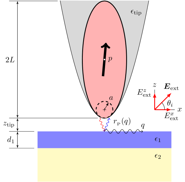
To make the calculations tractable, we follow examples in the literature Porto et al. (2003); Renger et al. (2005); Esteban et al. (2009) and model the tip as a metallic spheroid of total length , see Fig. 1. As shown below, this gives results in a much better agreement with the experiment in terms of both the frequency and the thickness dependence of the near-field signal. We attribute the origin of the more gradual film-thickness dependence in the spheroidal model to the aforementioned “antenna effect.” The magnitude of this effect is determined by the material response over length scales ranging from to , and so it truly saturates only when the film thickness becomes much larger than .
II Experiment
To make the paper self-contained we summarize the results of our recent experiments Andreev et al. in this Section. We investigated commercially available calibration gratings, which contain strips or islands of SiO2 thermally grown on Si. The manufacturer specified thicknesses of the SiO2 layer spanned the range , , , , and . A combination of CO2 and tunable quantum cascade lasers (Daylight Solutions) allowed us to cover the frequency range between 890 and 1250 . The near-field data were collected using a Neaspec system.
The measured s-SNOM signal represents the electromagnetic field backscattered by the probe and the scanned sample. The complex amplitude of the backscattered field varies periodically with the tapping frequency as the distance between the sample and the nearest point of the tip undergoes harmonic oscillations
| (1) |
where typically. In order to suppress unwanted background and isolate the part of the signal scattered by the probe tip, the signal is demodulated. Namely, we extracted the absolute values and phases at tapping harmonics
| (2) |
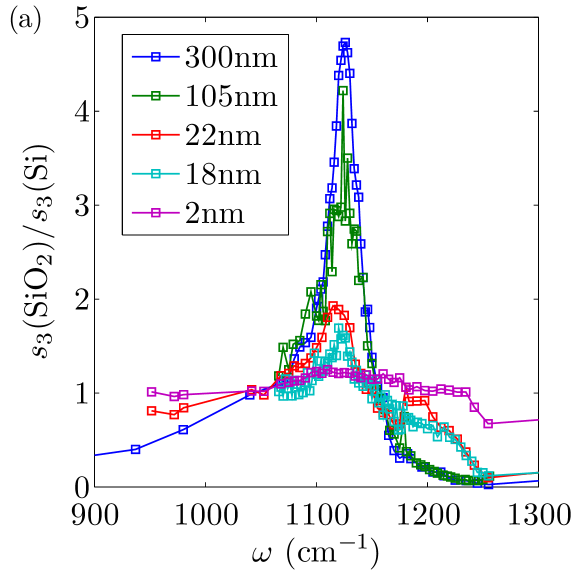
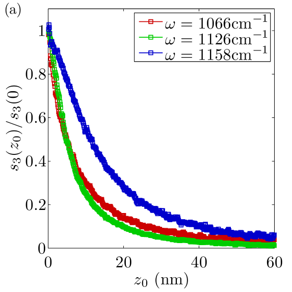
The experimental results for the spectra are shown in Fig. 2(a). These spectra were intended to be taken in the tapping mode, i.e., for zero . However, experimentally can be determined only up to an additive constant . Therefore, we measured -dependence of (the approach curves) shown in Fig. 3(a) and selected the largest observed . Our results are in a qualitative agreement with previous experimental study, Taubner et al. (2005) which reported approach curves for SiO2 at a few discrete frequencies and film thicknesses.
The data points in Fig. 2(a) represent the normalized amplitude , where and are the raw third-order demodulation signals averaged over the entire SiO2 and Si areas, respectively. The statistical uncertainty of these averaged data traces is about .
For each thickness studied, the normalized amplitude exhibits several maxima. The main peak is situated at . The key aspect of the data is a rapid decrease in the normalized amplitude of this peak as the thickness is reduced. A trace of this resonance can be reliably identified even for the -nm thick SiO2 film. Another notable feature is the growing strength and frequency shift of the secondary peaks on the high- side of the main peak as is decreased.
Since the response of Si is frequency independent in our experimental range, the frequency dependence of the spectra in Fig. 2(a) originates from that of SiO2. We attribute the maxima of to the phonon modes localized at the air-SiO2 interface. Amarie and Keilmann (2011) These resonances occur in the frequency region between the bulk transverse and longitudinal modes of SiO2 (the outer dashed lines in Fig. 4 below).
III Response functions and collective modes
The sample is modeled as a two-layer system. The first layer with dielectric function occupies the slab . The second layer with dielectric function occupies the half-space . The half-space (“layer 0”) is filled with air (dielectric constant ). The fundamental response functions of the system are the reflection coefficients , which are functions of in-plane momentum , frequency , and polarization or . The domain of definition of is understood to include nonradiative modes . It is known from previous studies that the s-SNOM signal is dominated by the -polarized waves. In our two-layer model their reflection coefficient is given by a Fresnel-like formula
| (3) | ||||
| (4) |
where -axis momenta are defined by
| (5) |
Equation (3) is valid for arbitrary . In the near-field case where is large and , it simplifies to
| (6) |
Assuming all are -independent, the effective dielectric function depends on only via the product in this limit. Therefore, for one thickness can be obtained from another by rescaling . As discussed in Sec. I and shown in more detail below, the most important momenta are where is the tip radius. Therefore, we can get an approximate understanding of the system response by examining the behavior of as a function of at fixed . This behavior is dictated by the spectrum of surface collective modes, as follows.
In general, surface modes correspond to poles of the response functions . Function given by Eq. (6) can have up to two poles at each , see, e.g., Ref. Prade et al., 1991. They are defined by the following condition on :
| (7) |
At large , where , this condition yields or , which correspond to modes localized at the upper – and the lower – interfaces, respectively. Actually, the latter “pole” has vanishingly small residue because evanescent waves do not reach the lower interface at . There is no -dispersion and no coupling of the two modes in this limit. The dispersion appears at finite , where the two modes become mixed. In particular, we find
| “0–1” | (8a) | ||||
| “1–2” | (8b) | ||||
at . At finite , both interfaces participate in generating these excitations. The labels “0–1” and “1–2” are for convenience: they indicate at which interface a given dispersion branch is ultimately localized as increases. At , the “0–1” and “1–2” branches are characterized by and , which correspond, respectively, to the bulk longitudinal and transverse phonon frequencies and .
If we try to apply this formalism to real materials, we face the problem that Eq. (7) has no solutions for real because the dielectric functions have finite imaginary parts. This is why in practice the collective mode spectra are usually defined differently. They are identified with the maxima of dissipation, i.e., . The number of these maxima can be fewer than the total allowed number of the modes because some of them can be overdamped. Similarly, we define and as the frequencies that correspond to the maxima of and .
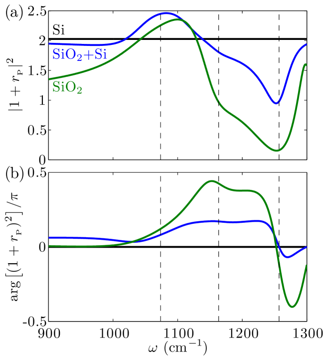
To see what kind of spectra are realized in our system, we use our ellipsometry data for [Fig. 4(a)] and Eq. (6) to compute for several values of . The plot of these quantities as a function of is presented in Fig. 4(c). Three maxima on each curve in the region of primary interest are apparent. They exist already at , and so all of them belong to the upper (air-SiO2) interface. In fact, we do not expect sharp modes at the lower (SiO2-Si) interface because the dielectric function of Si is quite large in the studied range of . The lowest value of is not sufficient to compensate and generate “1-2” modes, cf. Eq. (7).
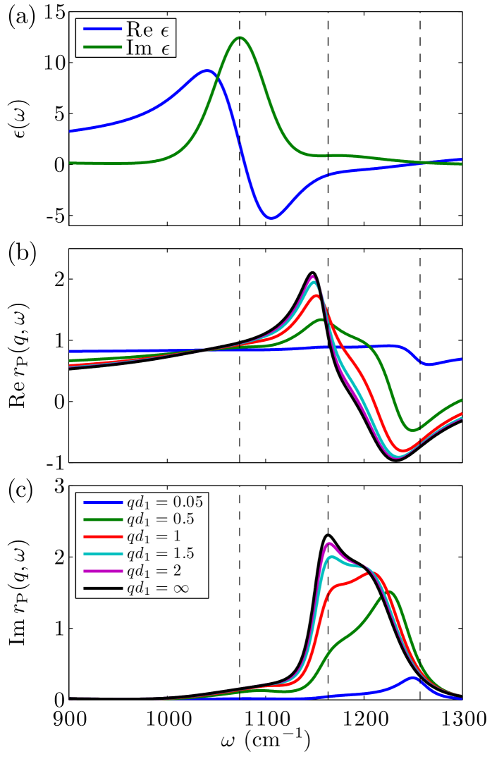
The main peak of at defines the surface phonon frequency of SiO2 . There also exist secondary peaks at and . Their evolution as a function of comply with the general scheme outlined above. As decreases, all the three peaks loose strength, as expected, because the amount of SiO2 diminishes. The lower- secondary peak redshifts, moving towards , and then quickly disappears. This agrees with the SiO2-Si resonance being highly damped. The higher- secondary peak becomes dominant at and demonstrates a systematic shift towards , see Fig. 4(c).
A notable feature of Fig. 4(b) is the clustering of the crossing points of the different curves near . This is the frequency where the dielectric function of SiO2 is the closest to that of Si, . As a result, the two layers act almost as one bulk material, so that is approximately thickness-independent.
There is a qualitative correspondence between the features displayed by the reflection coefficient and the observed near-field signal , cf. Figs. 2(a) and 4(b),(c). However, the relation between and the measured s-SNOM signal is nontrivial. For example, the frequency positions of the maxima in and those in differ by as much as . We also suspect that there may be some slight differences between the optical constants of thick films we assume in our calculations and those of the small SiO2 structures we probe by the s-SNOM. This is the likely reason why the crossing point of the experimental curves occurs near rather than predicted by both our models, cf. Fig. 2.
Developing a reliable procedure for inferring from remains a challenge for the theory. The next section presents our current approach towards this ultimate goal.
IV Tip-sample interaction
Both radiative and nonradiative waves may play significant roles in the s-SNOM experiment. Porto et al. (2003) The radiative modes magnify the signal by a certain far-field factor (FFF) , where is the momentum of these modes for the angle of incidence . The nonradiative modes influence the effective polarizability of the tip, i.e., the ratio of its dipole moment and the external electric field . Altogether the demodulated s-SNOM signal can be written as
| (9) | ||||
| (10) |
Below we discuss the FFF and the tip polarizability separately.
IV.1 Far-field factor
The FFF for an infinite layered system is given by Sukhov (2004); Aizpurua et al. (2008)
| (11) |
As shown in Figs. 5(a), for SiO2 film, the absolute value of the FFF has a maximum near and a suppression near . For thinner films, these features are less pronounced. The main maximum of , which is the main focus of our analysis, is away from both and . It is essentially unaffected by the FFF. Still, if FFF were to be included in the calculation in the form prescribed by Eq. (11), it would produce a visible hump of near and a dip near . These features are not present in the experimental data, Fig. 2(a). A better agreement with the experiment is obtained if is set to a constant, which is what we do here. We rationalize this decision by noting that the SiO2 layer in the actual samples does not extend over the entire – plane but occupies only small sub-wavelength regions. Therefore, the FFF is dominated by the -independent response of Si.
IV.2 Point-dipole model of the tip
The effective tip polarizability is the most important factor on the right-hand side of Eq. (9) and it is also the most difficult one to compute. This quantity is dictated by the near-field coupling between the tip and the sample. For irregular tip shapes it can be calculated only numerically. However, previous s-SNOM studies demonstrated that acceptable results can often be obtained if the tip is approximated by a spheroid, Porto et al. (2003); Renger et al. (2005); Esteban et al. (2009) a small sphere, Rendell and Scalapino (1981); Aravind and Metiu (1982, 1983); Ruppin (1992); Sukhov (2004); Renger et al. (2005) a “finite” dipole, Cvitkovic et al. (2007); Amarie and Keilmann (2011) or a point dipole. Hillenbrand and Keilmann (2000); Taubner et al. (2004); Aizpurua et al. (2008) The actual tip shape in our experiment is close to a rounded pyramid.
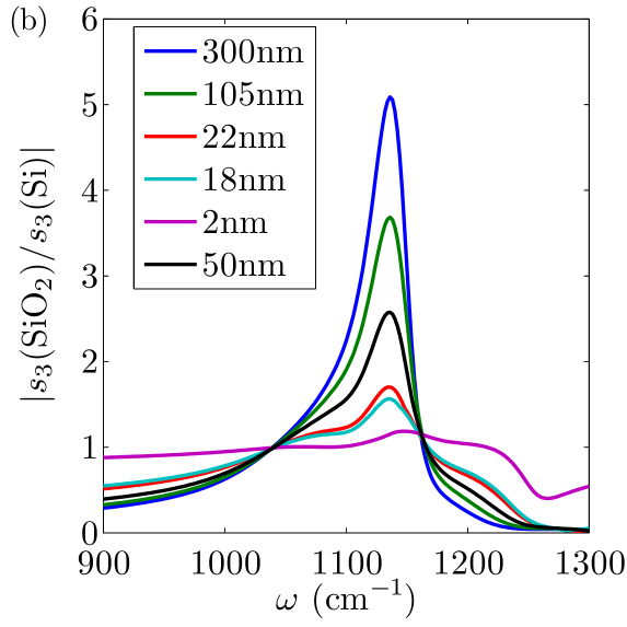
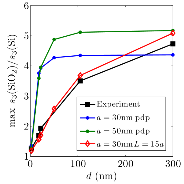
The point-dipole approximation is the simplest one and it has been used extensively for modeling s-SNOM experiments, including those performed on multilayer systems. Aizpurua et al. (2008); Fei et al. (ress) The point-dipole model has two adjustable parameters: the polarizability of the effective dipole and its position with respect to the bottom of the tip. The results obtained following the standard analysis Aizpurua et al. (2008); Fei et al. (ress) are shown in Fig. 2(c) using and . We see that even for this rather large the point-dipole model does not reproduce the observed strong dependence of on thickness at .
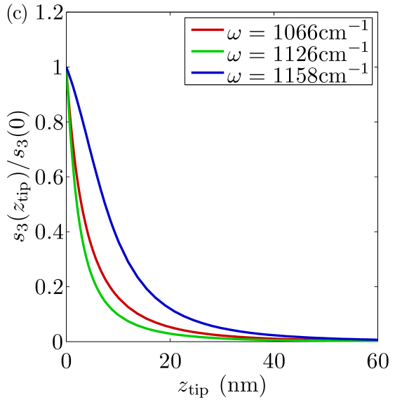
The discrepancy can be seen more clearly in Fig. 6, where the height of the peak in corresponding to the surface phonon is plotted as a function of . For the point dipole model the curve flattens at . In contrast, the experimentally observed maximum continues to rise with . The point-dipole model also predicts a very steep approach curve, Fig. 3(c), in poor agreement with the measurements.
The physical origin of the saturation of the thickness dependence in Fig. 2(c) is easy to understand. One can think about the near-field coupling between the point dipole and the sample in terms of the method of images. For a dipole positioned at , the image is concentrated at the depth below the surface. Therefore, films of thickness larger than would act as a bulk material. Another way to arrive at the same conclusion is to notice that the characteristic range of momenta of the relevant nonradiative waves is . Since depends on through the term [Eq. (6)], the dependence of the near-field coupling on should saturate at .
IV.3 Spheroid model of the tip
The lack of saturation in the observed s-SNOM signal as a function of at indicates that evanescent waves with momenta also play an important role in the near-field coupling between the tip and the sample. This is a signature of models in which the tip has a finite extent in space , see Fig. 1. Although such models are certainly more realistic than a point-dipole approximation, there has not been a systematic study of how the results would depend on the exact shape of the tip. Given some initial success of the point-dipole approximation, we speculate that a suitable simple shape can provide a good compromise between increase in computational effort and ability to capture relevant physics.
To test this idea, we model the tip as an elongated metallic spheroid positioned above a two-layer medium. This follows a tradition in the literature wherein similar models were considered Porto et al. (2003); Renger et al. (2005); Esteban et al. (2009) for the case of bulk substrates. In Ref. Cvitkovic et al., 2007 an analytical formula for the spheroidal tip was also proposed, based on heuristic arguments. However, it cannot be easily extended to the -dependent we study here. Instead, our calculations are done numerically. They involve only two essential approximations. One is neglecting retardation, which is justified is the length of the spheroid is smaller than . The other one is neglecting the finite skin depth of the metal (Pt-Ir alloy) covering the tip. Due to computational difficulties involved, this issue is left for future investigation.
The calculations were performed in two ways. First is the standard boundary-element method. In this method we divide the entire tip — assuming azimuthal symmetry — into a large number (typically, 200) of small cylindrical segments. We assume that different segments interact by Coulomb interaction as coaxial rings. The interaction of each segment with itself is defined in such a way that the polarizability of the tip in the absence of the sample coincides with the known analytical result for the prolate spheroid. The effect of the sample is included by adding ring-ring interactions mediated by reflected electrostatic fields. This is accomplished by numerical quadrature over the product of and suitable form-factors. This is the most time-consuming step of the simulation. After the interaction kernel is generated in this way, it is straightforward to solve numerically for the dipole moment of the tip induced by a unit external field, which is the desired polarizability .
We also developed a second numerical method of computing (to be described elsewhere), based on an expansion of the electric field in ellipsoidal harmonics. This alternative method is similar to that used for a metallic sphere above a dielectric half-space. Ford and Weber (1984); Sukhov (2004) We verified that the two methods give identical results.
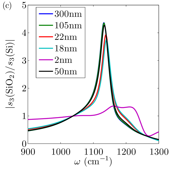
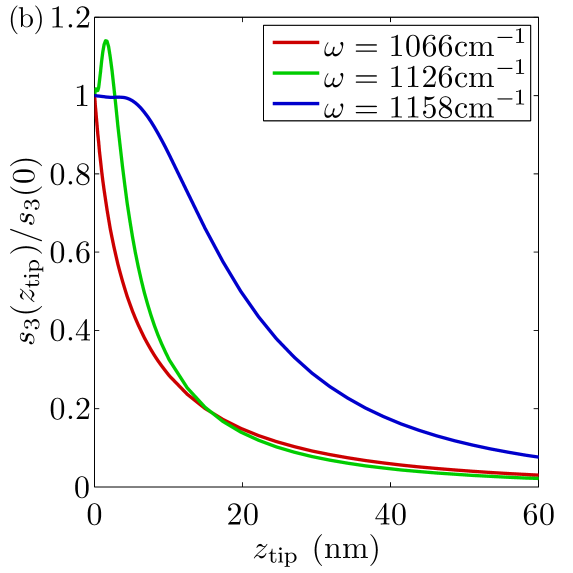
Substituting the computed polarizability into Eqs. (9) and demodulating per Eq. (10), we obtain approach curves. Figure 3(b) illustrates that some approach curves are nonmonotonic near the resonances. In calculating the s-SNOM amplitude we choose that corresponds to the largest because this is how it was done in the experiments. The results for the normalized amplitude are plotted in Fig. 2(b).
The spheroid model has two adjustable parameters: the apex radius of curvature and the half-length . When the spheroid becomes a sphere. In this case the spheroid model gives results similar to the point-dipole model, i.e., Fig. 2(c). As the ratio increases, the differences appear. However, once exceeds ten, the normalized signal does not change much at . Therefore, for long spheroids we effectively have only a single adjustable parameter, . Remarkably, the thickness dependence of the peak for the spheroid model matches the experiment extremely well (Fig. 6).
V Conclusions
In this paper we analyzed the results of experimental study of amorphous SiO2 films on Si obtained by scanning near-field optical spectroscopy. Andreev et al. We discussed the collective mode spectra of such structures and compared measurements with two theoretical calculations. The first is based on a conventional approximation in which the tip of the scanned probe is modeled as a point dipole. In the second the tip is treated as an elongated spheroid, significantly improving agreement with the experiment.
We explain the qualitative difference between the two models as follows. An important physical ingredient missing in the point-dipole model is the enhancement of the electric field near the apex of the tip — the antenna effect. This phenomenon is well-known from classical electrostatics. The enhancement of the field is controlled primarily by the ratio of the total length of the tip (actually, the smaller of and ) and the apex radius of curvature . The point-dipole model has been successful in the past without this enhancement factor only on account of the normalization procedure. Instead of absolute , one usually reports normalized to some reference material such as Au or in our case, Si. This way, one eliminates any possible frequency dependence of the source radiation, but at the same time cancels the part of the signal scaling with tip size. For a stratified sample this cancellation is imperfect because the the field enhancement depends also on the dielectric response of the sample, which is a function of momentum . For a tip of length , harmonics relevant for the field enhancement have momenta ranging from down to . Therefore, one may expect that the dependence of the s-SNOM signal on the thickness of the top layer would saturate only when . Our simulations provide direct evidence for this claim. Therefore, we think that the spheroid model holds a great promise as an analysis tool for near-field experiments. It captures a lot of physics relevant to the near-field interaction while remaining computationally fast.
The strong experimentally observed thickness dependence of the near-field signal Andreev et al. indicates that s-SNOM is capable of not only high lateral resolution but can also probe the system in the third dimension. However, the response of a layered system is different from those containing small subsurface particles Taubner et al. (2005). We hope that experimental and theoretical approaches presented in this paper may be of use for accurate depth profiling of various dielectric and metallic nanostructures.
The work at UCSD is supported by ONR, AFOSR, NASA, and UCOP. AHCN and LMZ acknowledge DOE grant DE-FG02-08ER46512 and ONR grant MURI N00014-09-1-1063. We thank F. Keilmann and R. Hillenbrand for illuminating discussions.
References
- Keilmann and Hillenbrand (2004) F. Keilmann and R. Hillenbrand, Phil. Trans. Roy. Soc. London, Ser. A 362, 787 (2004).
- Novotny and Hecht (2006) L. Novotny and B. Hecht, Principles of Nano-Optics (Cambridge University Press, 2006).
- Keilmann and Hillenbrand (2009) F. Keilmann and R. Hillenbrand, “Nano-optics and Near-field Optical Microscopy,” (Artech House, Norwood, 2009) Chap. 11: Near-Field Nanoscopy by Elastic Light Scattering from a Tip, pp. 235–266, edited by A. Zayats and D. Richards.
- Basov et al. (2011) D. N. Basov, R. D. Averitt, D. van der Marel, M. Dressel, and K. Haule, Rev. Mod. Phys. 83, 471 (2011).
- Basov and Chubukov (2011) D. N. Basov and A. V. Chubukov, Nat. Phys. 7, 272 (2011).
- Amarie and Keilmann (2011) S. Amarie and F. Keilmann, Phys. Rev. B 83, 045404 (2011).
- Huth et al. (2011) F. Huth, M. Schnell, J. Wittborn, N. Ocelic, and R. Hillenbrand, Nat. Mat. 10, 352 (2011).
- Qazilbash et al. (2007) M. M. Qazilbash, M. Brehm, B.-G. Chae, P.-C. Ho, G. O. Andreev, B.-J. Kim, S. J. Yun, A. V. Balatsky, M. B. Maple, F. Keilmann, H.-T. Kim, and D. N. Basov, Science 318, 1750 (2007).
- Zhan et al. (2007) H. Zhan, V. Astley, M. Hvasta, J. A. Deibel, D. M. Mittleman, and Y.-S. Lim, App. Phys. Lett. 91, 162110 (2007).
- Qazilbash et al. (2009) M. M. Qazilbash, M. Brehm, G. O. Andreev, A. Frenzel, P.-C. Ho, B.-G. Chae, B.-J. Kim, S. J. Yun, H.-T. Kim, A. V. Balatsky, O. G. Shpyrko, M. B. Maple, F. Keilmann, and D. N. Basov, Phys. Rev. B 79, 075107 (2009).
- Frenzel et al. (2009) A. Frenzel, M. M. Qazilbash, M. Brehm, B.-G. Chae, B.-J. Kim, H.-T. Kim, A. V. Balatsky, F. Keilmann, and D. N. Basov, Phys. Rev. B 80, 115115 (2009).
- Lai et al. (2010) K. Lai, M. Nakamura, W. Kundhikanjana, M. Kawasaki, Y. Tokura, M. A. Kelly, and Z.-X. Shen, Science 329, 190 (2010).
- Qazilbash et al. (2011) M. M. Qazilbash, A. Tripathi, A. A. Schafgans, B.-J. Kim, H.-T. Kim, Z. Cai, M. V. Holt, J. M. Maser, F. Keilmann, O. G. Shpyrko, and D. N. Basov, Phys. Rev. B 83, 165108 (2011).
- Fei et al. (ress) Z. Fei, G. O. Andreev, W. Bao, L. M. Zhang, Z. Zhao, G. Dominguez, M. Thiemens, M. M. Fogler, A. H. Castro Neto, C. N. Lau, F. Keilmann, and D. N. Basov, Nano Lett. (in press).
- Lai et al. (2007) K. Lai, M. B. Ji, N. Leindecker, M. A. Kelly, , and Z. X. Shen, Rev. Sci. Instrum. 78, 063702 (2007).
- Huber et al. (2008) A. J. Huber, F. Keilmann, J. Wittborn, J. Aizpurua, and R. Hillenbrand, Nano Lett. 8, 3766 (2008), pMID: 18837565.
- Olmon et al. (2008) R. L. Olmon, P. M. Krenz, A. C. Jones, G. D. Boreman, and M. B. Raschke, Opt. Express 16, 20295 (2008).
- Taubner et al. (2005) T. Taubner, F. Keilmann, and R. Hillenbrand, Opt. Express 13, 8893 (2005).
- (19) G. O. Andreev et al., “Infrared nanooptics of ultrathin materials,” in preparation.
- Hillenbrand et al. (2002) R. Hillenbrand, T. Taubner, and F. Keilmann, Nature 418, 159 (2002).
- Cvitkovic et al. (2007) A. Cvitkovic, N. Ocelic, and R. Hillenbrand, Opt. Express 15, 8550 (2007).
- Moon et al. (2011) K. Moon, E. Jung, M. Lim, Y. Do, and H. Han, Opt. Express 19, 11539 (2011).
- Porto et al. (2003) J. A. Porto, P. Johansson, S. P. Apell, and T. López-Ríos, Phys. Rev. B 67, 085409 (2003).
- Renger et al. (2005) J. Renger, S. Grafström, L. M. Eng, and R. Hillenbrand, Phys. Rev. B 71, 075410 (2005).
- Esteban et al. (2009) R. Esteban, R. Vogelgesang, and K. Kern, Opt. Express 17, 2518 (2009).
- Prade et al. (1991) B. Prade, J. Y. Vinet, and A. Mysyrowicz, Phys. Rev. B 44, 13556 (1991).
- Sukhov (2004) S. V. Sukhov, Ultramicroscopy 101, 111 (2004).
- Aizpurua et al. (2008) J. Aizpurua, T. Taubner, F. J. G. de Abajo, M. Brehm, and R. Hillenbrand, Opt. Express 16, 1529 (2008).
- Rendell and Scalapino (1981) R. W. Rendell and D. J. Scalapino, Phys. Rev. B 24, 3276 (1981).
- Aravind and Metiu (1982) P. K. Aravind and H. Metiu, J. Phys. Chem. 86, 5076 (1982).
- Aravind and Metiu (1983) P. K. Aravind and H. Metiu, Surf. Sci. 124, 506 (1983).
- Ruppin (1992) R. Ruppin, Phys. Rev. B 45, 11209 (1992).
- Hillenbrand and Keilmann (2000) R. Hillenbrand and F. Keilmann, Phys. Rev. Lett. 85, 3029 (2000).
- Taubner et al. (2004) T. Taubner, F. Keilmann, and R. Hillenbrand, Nano Lett. 4, 1669 (2004).
- Ford and Weber (1984) G. Ford and W. Weber, Physics Reports 113, 195 (1984).