Observation of Impurity-Induced Scale-Free Localization
in a Disordered Non-Hermitian Electrical Circuit
Abstract
One of unique features of non-Hermitian systems is the extreme sensitive to their boundary conditions, e.g., the emergence of non-Hermitian skin effect (NHSE) under the open boundary conditions, where most of bulk states become localized at the boundaries. In the presence of impurities, the scale-free localization can appear, which is qualitatively distinct from the NHSE. Here, we experimentally design a disordered non-Hermitian electrical circuits in the presence of a single non-Hermitian impurity and the nonreciprocal hopping. We observe the anomalous scale-free accumulation of eigenstates, opposite to the bulk hopping direction. The experimental results open the door to further explore the anomalous skin effects in non-Hermitian electrical circuits.
I Introduction
Growing efforts have been invested to intriguing phenomenon of non-Hermitian systems in recent year Ashida et al. (2020); Lee (2016); Leykam et al. (2017); Xu et al. (2017); Gong et al. (2018); El-Ganainy et al. (2018); Yao and Wang (2018); Zhang et al. (2020); Yokomizo and Murakami (2019); Yao et al. (2018); Kunst et al. (2018); Liu et al. (2019); Song et al. (2019); Zhang et al. (2021a); Lee et al. (2019); Kawabata et al. (2019a); Lee et al. (2019); Sun et al. (2021); Ge et al. (2019); Zhou and Lee (2019); Zhao et al. (2019); Kawabata et al. (2019b); Borgnia et al. (2020); Liu et al. (2020); Li et al. (2020); Yokomizo and Murakami (2021); Okuma et al. (2020); Zou et al. (2023); Fan and Liang (2021); Yi and Yang (2020); Liu et al. (2021); Li et al. (2021); Bergholtz et al. (2021); Li et al. (2022); Zhang et al. (2022a); Lin et al. (2023); Ren et al. (2022); Kawabata et al. (2023); Zhang et al. (2023a); Li et al. (2023a); Liu et al. (2023); Cai et al. (2024); Li et al. (2024); Cai et al. (2024); Liu et al. (2023); Li et al. (2024); Hu et al. (2024); Wang et al. (2024); Xie et al. (2024a); Zhang et al. (2024). One of unique features in non-Hermitian systems is the non-Hermitian skin effect (NHSE) Yao and Wang (2018); Zhang et al. (2020); Yokomizo and Murakami (2019); Yao et al. (2018); Kunst et al. (2018); Liu et al. (2019); Song et al. (2019). This effect is characterized by an extreme sensitivity of eigenspectra to boundary conditions, where most of bulk modes become localized at the boundaries under open boundary conditions (OBCs). A lot of exciting non-Hermitian phenomena without their Hermitian counterparts are related to the NHSE, e.g., breakdown of conventional Bloch band theory Yao and Wang (2018), scale-free localization Li et al. (2021), and disorder-free entanglement phase transitions Kawabata et al. (2023). The NHSEs have been experimentally observed in many physical systems and have also shown potential applications in sensors due to the extreme sensitivity to the boundary conditions Koch and Budich (2022); Budich and Bergholtz (2020); McDonald and Clerk (2020) .
For NHSE, the localization length of bulk modes is usually independent of the system’s size under OBCs. Recently, an anomalous skin localization, dubbed scale-free localization, was found and extensively explored in non-Hermitian system Li et al. (2021); Guo et al. (2023); Li et al. (2023b); Wang et al. (2023); Yokomizo and Murakami (2021); Fu and Zhang (2023); Xie et al. (2024b); Molignini et al. (2023). Unlike the conventional NHSE, the localization length of scale-free modes relies on the system size, and the localization direction is not indicated by the bulk. This intriguing localization phenomenon has been largely investigated in various non-Hermitian systems Li et al. (2021); Guo et al. (2023); Li et al. (2023b); Wang et al. (2023); Yokomizo and Murakami (2021); Fu and Zhang (2023); Xie et al. (2024b); Molignini et al. (2023). Recently, the scale-free localization has been experimentally observed in an electrical circuit with a Hermitian lattice subjected to a parity-time-symmetric non-Hermitian defect Xie et al. (2024b). While, the experimental observation of the scale-free localization, resulting from the interplay of nonreciprocal hopping in the bulk and the single impurity, is still lacking.
An electrical circuit has become a powerful platform to realize topological structures even with complicated lattice geometries, e.g., higher-order topological Anderson insulator, novel topological states in hyperbolic lattices, and among others Zhang et al. (2021b, 2023b); Imhof et al. (2018); Zangeneh-Nejad and Fleury (2019); Serra-Garcia et al. (2019); Zhang et al. (2023c, 2022b). Due to the design flexibility, the nonreciprocal hopping can be easily realized by using operational amplifiers arranged as impedance converters through current inversion (INIC) Hofmann et al. (2019). Therefore, the electrical circuits have been utilized to realize novel non-Hermitian phenomena Lee et al. (2018); Helbig et al. (2019); Hofmann et al. (2019); Zhang et al. (2019); Wang et al. (2020); Bao et al. (2019); Lu et al. (2019). In this work, we experimentally designed the non-Hermitian electrical circuit in the presence of the nonreciprocal hopping, a single non-Hermitian impurity and onsite disorder. We measure and observe the scale-free localization in the disordered non-Hermitian chain. Such anomalous scale-free accumulations of eigenstates are controlled by the single non-Hermitian impurity, and their localization direction can be opposite to the bulk hopping direction. Our experiment verifies the existence of the anomalous skin effects induced by the single impurity in the nonreciprocal systems, and the results open the door to further explore the interesting localization phenomena in non-Hermitian electrical circuits.
II Model and Non-Hermitian electrical circuit
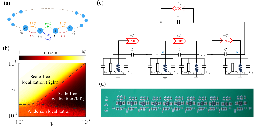
In order to study the anomalous skin effect due to the interplay of disorder and impurity, we consider the disordered Hatano-Nelson (HN) chain in the presence of a single non-Hermitian impurity, with its Hamiltonian reading Molignini et al. (2023)
| (1) |
where indicate the asymmetric hopping strengths, is onsite disorder potential, sampled in a random uniform distribution , and are the asymmetric hopping strengths between the first and last sites, severing as a single non-Hermitian impurity [see Fig. 1(a)]. By controlling the impurity’s parameters in the presence of the disorder, one can observe anomalous skin-localization phenomena Molignini et al. (2023), where the system undergoes Anderson localization and scale-free skin localization, as indicated by the phase diagram in Fig. 1(b). The phase diagram is obtained by calculating the mean center of mass (mcom), which is defined as the amplitude squared of all right eigenvectors , averaged over many disorder realizations Molignini et al. (2023), i.e.,
| (2) |
with
| (3) |
Here, indicates disorder averages.
The nonreciprocal hopping typically leads to non-Hermitian skin effects in the clean system. While, the scale-free localization in the presence of a single non-Hermitian impurity is distinct from the non-Hermitian skin effect, where its localization is not dictated by the bulk, and the localization length is proportional to the system size Molignini et al. (2023). Furthermore, the localization at the left or right boundary of the chain is controlled by the impurity hopping strength in the 1D disordered HN chain [see Fig. 1(b)]. Note that such anomalous skin-localization feature is determined by the interplay of bulk hopping strength and the single non-Hermitian impurity, but it is stabilized to a nonmonotonic localization behavior as a function of the hopping terms by the random disorder Molignini et al. (2023), as shown in Fig. 1(b).
In order to experimentally observe the anomalous skin-localization phenomena due to the interplay of a single non-Hermitian impurity and the bulk nonreciprocal hopping, we design non-Hermitian electrical circuits, corresponding to the model in Eq. (II). Figure 1(c) plots the electrical circuit network, where the nonreciprocal hopping between nodes and is realized by the negative impedance converters through current inversions (INICs) Hofmann et al. (2019). Figure 1(d) shows the experimental circuit board, where the first node and the last node are connected by the external wires acting as the single non-Hermitian impurity. The disorder term in Eq. (II) is introduced by the grounded capacitor () and the tolerance of the grounded inductance [see Fig. 1(c)]. The model in Eq. (II) is represented by the circuit Laplacian of the circuit Lee et al. (2018). The Laplacian is defined as the grounded-voltage vector to the vector of input current by . As shown in Fig. 1(c), the circuit Laplacian reads (see Appendix A)
| (4) |
with
| (5) |
where signifies a grounded capacitor at the node within the range . By further writing as , one found that and share the same eigenstates, if we set , , and . The eigenvalues and eigenstates of can be obtained by measuring the voltage response at the circuit nodes.
III Electrical-circuit simulation of scale-free localization
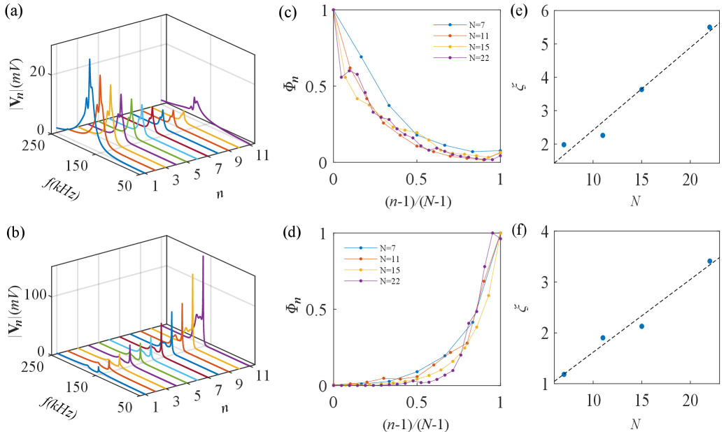
It has shown that the single non-Hermitian impurity can induce a scale-free accumulation of all eigenstates opposite to the bulk hopping direction [see Fig. 1(b)], distinct from the NHSE occurring at open boundaries Molignini et al. (2023). Such scale-free localization phenomenon is simulated using electrical circuit, as shown in Fig. 2. Here, we set , , and introduced onsite disorder through random variations in the fabricated grounded inductors due to imperfect manufacturing processes.
The voltage distribution at resonance frequency can be used to represent the state distribution of the circuit Laplacian. Figure 2(a,b) plots the frequency-resolved voltage distribution excited by alternating current (AC) at the different node for nF and nF, and (b) for nF and nF, corresponding to the skin-mode localized at the left and right sides of the chain, respectively. This indicates that the bulk states localized towards different directions can be controlled by changing the hopping strength within the bulk chain and the the hopping strength at the single-impurity site in spite of the nonreciprocal hopping direction within the bulk.
Figure 1(b) shows the existence of the scale-free localization controlled by the single non-Hermitian impurity in the presence of weak disorder, where the localization length is dependent on the lattice size. In order to demonstrate the scale-free localization, we calculate the normalized spatial distribution of the peak voltage at the node , which is defined as
| (6) |
where denotes the peak voltage at node , which is normalized to the maximum value of peak voltages of all the nodes.
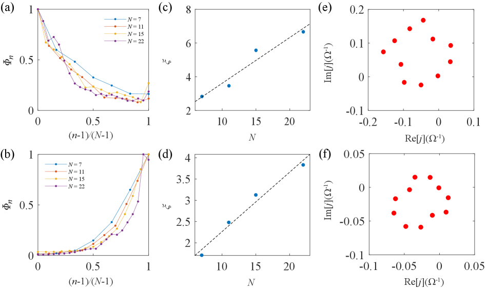
Figure 2(c,d) shows the normalized spatial distribution of the peak voltage as a function of the normalized node index for the left- and right-localized skin modes at the different lattice size , where the node index is mapped to the range . The state distributions at the different size are collapsed close to each other, indicating the size-dependent localization length. By exponentially fitting the state distribution, we extract the localization length at different lattice size [see blue dots in Fig. 2(e,f)]. After linearly fitting these dots, the localization length exhibits the linear dependence on the lattice size . This indicates the existence of the scale-free localization for the skin modes controlled by the single non-Hermitian impurity.
IV Experimental results of electrical circuits
Our main results are the experimental verification of the scale-free localization induced by the single non-Hermitian impurity Molignini et al. (2023) using the electrical circuit. The electrical-circuit network and fabricated experimental circuit board are shown in Fig. 1(c,d). As shown in Fig. 1(c), two nodes within the circuit are interconnected via capacitors and INICs, where the INICs have the equivalent capacitance of in opposite directions. The first and last nodes are connected through distinct capacitors and INICs, denoted as and , which serve as the single non-Hermitian impurity. The parameters of the experimental electrical circuits are the same as ones used in the simulation. In addition to the random variations suffering from imperfect manufacturing processes, disorder is mainly introduced by the grounded capacitors . The grounded capacitor of each node is randomly chosen from a diverse set of capacitors with capacitance ranging from to nF. The diagonal element of the circuit Laplacian is given by , and the circuit’s reference frequency reads , where the capacitance is nF for the left-localized states, corresponding to kHz, and it is nF for the right-localized states, corresponding to kHz. A chirp signal spanning the frequency band from kHz to kHz is used as the excitation. Details of the sample fabrication and experimental measurements are provided in the Appendix B.
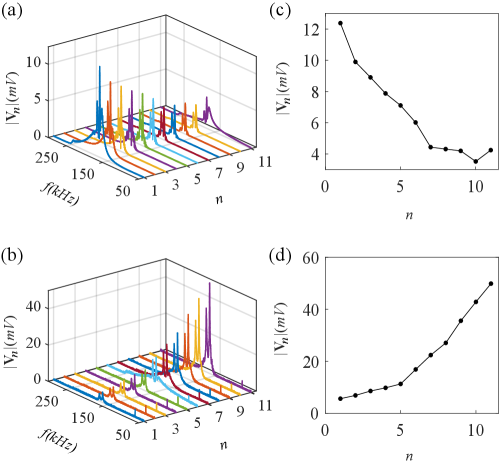
The experimentally measured voltages of the admittance under the excitation of chirp signals are shown in Fig. 3. We have experimentally designed two electrical circuits with different parameters of boundary capacitors acting as the single impurity, where the bulk parameters are fixed. To be specific, for the nF and nF, we plot the frequency-resolved voltage distribution [see Fig. 3(a)]. The voltage is peaked around the frequency of kHz, which matches well with the simulated result. By extracting the peak voltage at each node, its spatial distribution is shown in Fig. 3(b)], corresponding to the state distribution of non-Hermitian Hamiltonian for the specific eigenvalue. This state is localized at the left side, indicating the occurrence of NHSE. While, for nF and nF, the voltage is peaked around the frequency of kHz [see Fig. 3(b)], where we observe the right-side localized state [see Fig. 3(d)]. The experimental results indicate the existence of the anomalous skin-mode localization controlled by the single impurity in spite of the bulk hopping direction.
To verify the scale-free localization property, we measured the site-resolved peak voltages for different sizes, as shown in Fig. 4(a,b). For the left-side skin modes, the parameter of the impurity for all the samples is set as nF and nF, and for the right-side skin modes, it is nF and nF. Figure 4(a) plots the peak voltages of different samples as a function of normalized node index , where the node index is normalized to the range . These left-side skin modes are not collapsed, indicating the absence of scaled localization for nF and nF. There is also absence of scaled localization for right-side skin modes with the single-impurity parameters set as nF and nF. After performing a linear fit of the localization length at different sizes, we observe scale-free localization behavior. This size-dependence of the localization behavior exhibits a significant deviation from the NHSE, where the localization length remains consistent for different system size , as predicted in Refs. Molignini et al. (2023); Li et al. (2021). This unique phenomena of scale-free eigenstates are usually accompanied by the emergence of complex eigenspectrumLi et al. (2021), which has also been presented in Fig. 4(e,f).
V Conclusion
In summary, we have experimentally observed the anomalous non-Hermitian skin effects with skin-mode localization directions controlled by a single non-Hermitian impurity in non-Hermitian disordered electrical circuits. Furthermore, anomalous skin modes are verified to show the scale-free localization induced by the single non-Hermitian impurity by measuring the size-dependent localization length. Our experimental results have proved the theoretical proposal on the scale-free localization induced by the single non-Hermitian impurity. In the future, it would be interesting to investigate scale-free localization in higher dimensions.
Acknowledgements.
T.L. acknowledges the support from the Fundamental Research Funds for the Central Universities (Grant No. 2023ZYGXZR020), Introduced Innovative Team Project of Guangdong Pearl River Talents Program (Grant No. 2021ZT09Z109), and the Startup Grant of South China University of Technology (Grant No. 20210012). W.B.J is supported by the National Natural Science Foundation of China (NSFC) (Grant No. U21A2093).Appendix A Circuit Laplacian
Linear circuit networks, composed of linear components, can be characterized by a series of time-dependent differential equations. After applying the Fourier transformation with respect to the time, these equations can be simplified into a set of algebraic equations in the frequency domain Lee et al. (2018). In the frequency domain, the relation of current and voltage between two nodes can be written as
| (7) |
where is the impedance between node and node , and the impedances of capacitor, inductor and resistor are and . According to Kirchhoff’s current law, the sum of all currents entering and leaving a node equals zero. This indicates that the input current at the node equals the sum of the currents leaving node .
| (8) |
According to Eq. (7) and Eq. (8), we can derive the circuit Laplacian of the electrical circuit in Fig. 1(c,d). Two nearest-neighbor nodes are connected through capacitor with the capacitance , and grounded by a capacitor , an inductance and a resistance . Two nearest-neighbor nodes are also connected through an INIC in parallel. The INIC acts as a capacitance of in two opposite directions. The circuit equation of the th () node is written as,
| (9) |
The first and last nodes are connected via the capacitor with the capacitance , grounded by the capacitor , an inductance and a resistance . The circuit equations for the first and last nodes can be written as
| (10) |
and
| (11) |
In order to have the same on-site potential for all the nodes, we set and . Then, we achieve the circuit Laplacian as
| (12) |
where , and is the grounded capacitance ranging from 0 to , serving as disorder. If we set , , and , and can be related by .
Appendix B Details of experimental implementation
B.1 Experimental setup
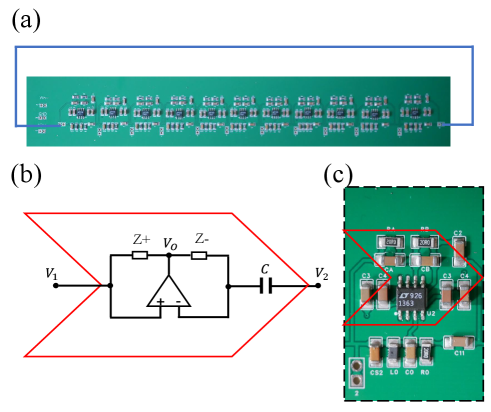
The disordered Hatano-Nelson model in the presence of a single non-Hermitian impurity is simulated by the grounded circuit Laplacian of the electrical circuit in Fig. 1(c). The fabricated circuit board is shown in Fig. 5(a), where the nonreciprocal hopping is realized via utilizing the impedance converters with current inversion (INIC) [see Fig. 5(b)]. The circuit board of each unit cell is shown in Fig. 5(c), where the red dashed curve indicates the INIC.
As shown in Fig. 1(c), two nodes within the circuit are interconnected via capacitors and INICs, where the INICs exhibit equivalent capacitance of in opposite directions. The first and last nodes are connected through distinct capacitors and INICs, denoted as and ,which serve as the single impurity. Each node is grounded by an inductor H, a resistor , and capacitors nF and . In addition to the random variations suffering from imperfect manufacturing processes, the random on-site potential is mainly realized by disordered grounded capacitors with the capacitance of each node. The value of is randomly selected within the range from nF to nF.
The diagonal element of the circuit Laplacian is given by , which vanishes at frequency . In the experimental designs, the capacitance is chosen as nF for the left-localized states, corresponding to kHz. It is nF for the right-localized states, corresponding to kHz. They shows good consistency with the experimentally measured frequencies at the maximum voltage response, which were kHz and kHz, respectively.
For our specific experimental setup, a circuit board with capacitors, inductors and resistors and operational amplifier was implemented on a Printed Circuit Board (PCB). To ensure proper operation, the operational amplifier (LT1363) was powered by a DC current using the Keysight E3631A power supply. To reduce noise from the DC power supply, capacitors with capacitances of F and F were placed at the DC input of the operational amplifier. A chirp signal, covering a frequency range from kHz to 250 kHz, was generated using a Keysight 33500B waveform generator. The voltage source was interfaced with the Printed Circuit Board (PCB) through a shunt resistor , functioning as the current input. A current source was input into the PCB to capture the voltage response using a Keysight DSOX4052A oscilloscope. A Fast Fourier Transform (FFT) was then applied to the measured time-domain voltage to obtain the voltage response in the frequency domain.
B.2 Measurement
In this section, we introduce the measurement of observables in electrical circuitsHelbig et al. (2020, 2019). In our experiment, we measured the circuit’s voltage response and complex admittance. In following, we will discuss their correlation with the eigenvectors and eigenvalues of the Laplacian .
Voltage response— Based on , upon the input of the current, the voltage response at each node can be obtained by the inversion of Laplacian .
| (13) |
where is the th eigenvalue of , and is the right eigenvector of with eigenvalue while is the left eigenvector of . It indicates that all eigenstates contributes to voltage response, where each eigenstate’s contribution is weighted by its corresponding admittance and . The eigenvalue varies with frequency . Assuming that, at the specific frequency, has the eigenvalue very close to zero, the weight of the right eigenvector can be considered significantly larger than contributions from the other right eigenvectors. In this case, the voltage response behaves as
| (14) |
It indicates that, at this frequency, the voltage response of the circuit can be considered determined by the eigenvector .
Complex admittance— The voltage response depends on the inverse of the Laplacian and input current. Their relationship can be expressed as
| (15) |
is the inverse of the Laplacian . If we input a current at the single node , the the voltage response:
| (16) |
While we input a current at one node and measure the voltage response of all nodes, one can obtain a column of the matrix . By repeating this process times, we obtain . Consequently, the Laplacian can be achieved by inverting . The complex admittance is calculated using the reconstructed Laplacian .
References
- Ashida et al. (2020) Y. Ashida, Z. Gong, and M. Ueda, “Non-Hermitian physics,” Adv. Phys. 69, 249 (2020).
- Lee (2016) Tony E. Lee, “Anomalous edge state in a non-Hermitian lattice,” Phys. Rev. Lett. 116, 133903 (2016).
- Leykam et al. (2017) D. Leykam, K. Y. Bliokh, C. Huang, Y. D. Chong, and F. Nori, “Edge modes, degeneracies, and topological numbers in non-Hermitian systems,” Phys. Rev. Lett. 118, 040401 (2017).
- Xu et al. (2017) Y. Xu, S. T. Wang, and L. M. Duan, “Weyl exceptional rings in a three-dimensional dissipative cold atomic gas,” Phys. Rev. Lett. 118, 045701 (2017).
- Gong et al. (2018) Z. Gong, Y. Ashida, K. Kawabata, K. Takasan, S. Higashikawa, and M. Ueda, “Topological phases of non-Hermitian systems,” Phys. Rev. X 8, 031079 (2018).
- El-Ganainy et al. (2018) R. El-Ganainy, K. G. Makris, M. Khajavikhan, Z. H. Musslimani, S. Rotter, and D. N. Christodoulides, “Non-Hermitian physics and PT symmetry,” Nat. Phys. 14, 11 (2018).
- Yao and Wang (2018) S. Yao and Z. Wang, “Edge states and topological invariants of non-Hermitian systems,” Phys. Rev. Lett. 121, 086803 (2018).
- Zhang et al. (2020) K. Zhang, Z. Yang, and C. Fang, “Correspondence between winding numbers and skin modes in non-Hermitian systems,” Phys. Rev. Lett. 125, 126402 (2020).
- Yokomizo and Murakami (2019) K. Yokomizo and S. Murakami, “Non-Bloch band theory of non-Hermitian systems,” Phys. Rev. Lett. 123, 066404 (2019).
- Yao et al. (2018) S. Yao, F. Song, and Z. Wang, “Non-Hermitian Chern bands,” Phys. Rev. Lett. 121, 136802 (2018).
- Kunst et al. (2018) F. K. Kunst, E. Edvardsson, J. C. Budich, and E. J. Bergholtz, “Biorthogonal bulk-boundary correspondence in non-Hermitian systems,” Phys. Rev. Lett. 121, 026808 (2018).
- Liu et al. (2019) T. Liu, Y.-R. Zhang, Q. Ai, Z. Gong, K. Kawabata, M. Ueda, and F. Nori, “Second-order topological phases in non-Hermitian systems,” Phys. Rev. Lett. 122, 076801 (2019).
- Song et al. (2019) F. Song, S. Yao, and Z. Wang, “Non-Hermitian skin effect and chiral damping in open quantum systems,” Phys. Rev. Lett. 123, 170401 (2019).
- Zhang et al. (2021a) Y.-T. Zhang, S. Jiang, Q. Li, and Q.-F. Sun, “An analytical solution for quantum scattering through a PT-symmetric delta potential,” Front. Phys. 16, 43503 (2021a).
- Lee et al. (2019) J. Y. Lee, J. Ahn, H. Zhou, and A. Vishwanath, “Topological correspondence between Hermitian and non-Hermitian systems: Anomalous dynamics,” Phys. Rev. Lett. 123, 206404 (2019).
- Kawabata et al. (2019a) K. Kawabata, T. Bessho, and M. Sato, “Classification of exceptional points and non-Hermitian topological semimetals,” Phys. Rev. Lett. 123, 066405 (2019a).
- Sun et al. (2021) G. Sun, J.-C. Tang, and S.-P. Kou, “Biorthogonal quantum criticality in non-Hermitian many-body systems,” Front. Phys. 17, 33502 (2021).
- Ge et al. (2019) Z. Y. Ge, Y. R. Zhang, T. Liu, S. W. Li, H. Fan, and F. Nori, “Topological band theory for non-Hermitian systems from the Dirac equation,” Phys. Rev. B 100, 054105 (2019).
- Zhou and Lee (2019) H. Zhou and J. Y. Lee, “Periodic table for topological bands with non-Hermitian symmetries,” Phys. Rev. B 99, 235112 (2019).
- Zhao et al. (2019) H. Zhao, X. Qiao, T. Wu, B. Midya, S. Longhi, and L. Feng, “Non-Hermitian topological light steering,” Science 365, 1163 (2019).
- Kawabata et al. (2019b) K. Kawabata, K. Shiozaki, M. Ueda, and M. Sato, “Symmetry and topology in non-Hermitian physics,” Phys. Rev. X 9, 041015 (2019b).
- Borgnia et al. (2020) D. S. Borgnia, A. J. Kruchkov, and R.-J. Slager, “Non-Hermitian boundary modes and topology,” Phys. Rev. Lett. 124, 056802 (2020).
- Liu et al. (2020) T. Liu, J. J. He, T. Yoshida, Z.-L. Xiang, and F. Nori, “Non-Hermitian topological Mott insulators in one-dimensional fermionic superlattices,” Phys. Rev. B 102, 235151 (2020).
- Li et al. (2020) L. Li, C. H. Lee, S. Mu, and J. Gong, “Critical non-Hermitian skin effect,” Nat. Commun. 11, 5491 (2020).
- Yokomizo and Murakami (2021) K. Yokomizo and S. Murakami, “Scaling rule for the critical non-Hermitian skin effect,” Phys. Rev. B 104, 165117 (2021).
- Okuma et al. (2020) N. Okuma, K. Kawabata, K. Shiozaki, and M. Sato, “Topological origin of non-Hermitian skin effects,” Phys. Rev. Lett. 124, 086801 (2020).
- Zou et al. (2023) Y.-Y. Zou, Y. Zhou, L.-M. Chen, and P. Ye, “Detecting bulk and edge exceptional points in non-Hermitian systems through generalized Petermann factors,” Front. Phys. 19, 23201 (2023).
- Fan and Liang (2021) A. Fan and S.-D. Liang, “Complex energy plane and topological invariant in non-Hermitian systems,” Front. Phys. 17, 33501 (2021).
- Yi and Yang (2020) Y. Yi and Z. Yang, “Non-Hermitian skin modes induced by on-site dissipations and chiral tunneling effect,” Phys. Rev. Lett. 125, 186802 (2020).
- Liu et al. (2021) T. Liu, J. J. He, Z. Yang, and F. Nori, “Higher-order Weyl-exceptional-ring semimetals,” Phys. Rev. Lett. 127, 196801 (2021).
- Li et al. (2021) L. Li, C. H. Lee, and J. Gong, “Impurity induced scale-free localization,” Commun. Phys. 4, 42 (2021).
- Bergholtz et al. (2021) E. J. Bergholtz, J. C. Budich, and F. K. Kunst, “Exceptional topology of non-Hermitian systems,” Rev. Mod. Phys. 93, 015005 (2021).
- Li et al. (2022) Y. Li, C. Liang, C. Wang, C. Lu, and Y.-C. Liu, “Gain-loss-induced hybrid skin-topological effect,” Phys. Rev. Lett. 128, 223903 (2022).
- Zhang et al. (2022a) K. Zhang, Z. Yang, and C. Fang, “Universal non-Hermitian skin effect in two and higher dimensions,” Nat. Commun. 13, 2496 (2022a).
- Lin et al. (2023) R. Lin, T. Tai, L. Li, and C. H. Lee, “Topological non-Hermitian skin effect,” Front. Phys. 18, 53605 (2023).
- Ren et al. (2022) Z. Ren, D. Liu, E. Zhao, C. He, K. K. Pak, J. Li, and G.-B. Jo, “Chiral control of quantum states in non-Hermitian spin–orbit-coupled fermions,” Nat. Phys. 18, 385 (2022).
- Kawabata et al. (2023) K. Kawabata, T. Numasawa, and S. Ryu, “Entanglement phase transition induced by the non-Hermitian skin effect,” Phys. Rev. X 13, 021007 (2023).
- Zhang et al. (2023a) K. Zhang, C. Fang, and Z. Yang, “Dynamical degeneracy splitting and directional invisibility in non-Hermitian systems,” Phys. Rev. Lett. 131, 036402 (2023a).
- Li et al. (2023a) C.-A. Li, B. Trauzettel, T. Neupert, and S.-B. Zhang, “Enhancement of second-order non-Hermitian skin effect by magnetic fields,” Phys. Rev. Lett. 131, 116601 (2023a).
- Liu et al. (2023) J. Liu, Z.-F. Cai, T. Liu, and Z. Yang, “Reentrant non-Hermitian skin effect in coupled non-Hermitian and Hermitian chains with correlated disorder,” arXiv:2311.03777 (2023).
- Cai et al. (2024) Z.-F. Cai, T. Liu, and Z. Yang, “Non-Hermitian skin effect in periodically driven dissipative ultracold atoms,” Phys. Rev. A 109, 063329 (2024).
- Li et al. (2024) X. Li, J. Liu, and T. Liu, “Localization-delocalization transitions in non-Hermitian Aharonov-Bohm cages,” Front. Phys. 19, 33211 (2024).
- Hu et al. (2024) Y.-M. Hu, H.-Y. Wang, Z. Wang, and F. Song, “Geometric origin of non-Bloch symmetry breaking,” Phys. Rev. Lett. 132, 050402 (2024).
- Wang et al. (2024) H.-Y. Wang, F. Song, and Z. Wang, “Amoeba formulation of non-Bloch band theory in arbitrary dimensions,” Phys. Rev. X 14, 021011 (2024).
- Xie et al. (2024a) X.-D. Xie, Z.-Y. Xue, and D.-B. Zhang, “Variational quantum algorithms for scanning the complex spectrum of non-Hermitian systems,” Front. Phys. 19, 41202 (2024a).
- Zhang et al. (2024) H. Zhang, Z. Guo, Y. Li, Y. Yang, Y. Chen, and H. Chen, “A universal non-Hermitian platform for bound state in the continuum enhanced wireless power transfer,” Front. Phys. 19, 43209 (2024).
- Koch and Budich (2022) F. Koch and J. C. Budich, “Quantum non-hermitian topological sensors,” Phys. Rev. Res. 4, 013113 (2022).
- Budich and Bergholtz (2020) J. C. Budich and E. J. Bergholtz, “Non-hermitian topological sensors,” Phys. Rev. Lett. 125, 180403 (2020).
- McDonald and Clerk (2020) A. McDonald and A. A. Clerk, “Exponentially-enhanced quantum sensing with non-hermitian lattice dynamics,” Nat. Commun. 11, 5382 (2020).
- Guo et al. (2023) C.-X. Guo, X. Wang, H. Hu, and S. Chen, “Accumulation of scale-free localized states induced by local non-hermiticity,” Phys. Rev. B 107, 134121 (2023).
- Li et al. (2023b) B. Li, H.-R. Wang, F. Song, and Z. Wang, “Scale-free localization and symmetry breaking from local non-hermiticity,” Phys. Rev. B 108, L161409 (2023b).
- Wang et al. (2023) Y. Wang, J. Lin, and P. Xu, “Transmission-reflection decoupling of non-hermitian photonic doping epsilon-near-zero media,” Front. Phys. 19, 33206 (2023).
- Fu and Zhang (2023) Y. Fu and Y. Zhang, “Hybrid scale-free skin effect in non-hermitian systems: A transfer matrix approach,” Phys. Rev. B 108, 205423 (2023).
- Xie et al. (2024b) X. Xie, G. Liang, F. Ma, Y. Du, Y. Peng, E. Li, H. Chen, L. Li, F. Gao, and H. Xue, “Observation of scale-free localized states induced by non-hermitian defects,” Phys. Rev. B 109, L140102 (2024b).
- Molignini et al. (2023) P. Molignini, O. Arandes, and E. J. Bergholtz, “Anomalous skin effects in disordered systems with a single non-Hermitian impurity,” Phys. Rev. Res. 5, 033058 (2023).
- Zhang et al. (2021b) W. Zhang, D. Zou, Q. Pei, W. He, J. Bao, H. Sun, and X. Zhang, “Experimental observation of higher-order topological anderson insulators,” Phys. Rev. Lett. 126, 146802 (2021b).
- Zhang et al. (2023b) W. Zhang, H. Wang, H. Sun, and X. Zhang, “Non-abelian inverse anderson transitions,” Phys. Rev. Lett. 130, 206401 (2023b).
- Imhof et al. (2018) S. Imhof, C. Berger, F. Bayer, J. Brehm, L. W. Molenkamp, T. Kiessling, F. Schindler, C. H. Lee, M. Greiter, T. Neupert, and R. Thomale, “Topolectrical-circuit realization of topological corner modes,” Nat. Phys. 14, 925 (2018).
- Zangeneh-Nejad and Fleury (2019) F. Zangeneh-Nejad and R. Fleury, “Nonlinear second-order topological insulators,” Phys. Rev. Lett. 123, 053902 (2019).
- Serra-Garcia et al. (2019) M. Serra-Garcia, R. Süsstrunk, and S. D. Huber, “Observation of quadrupole transitions and edge mode topology in an lc circuit network,” Phys. Rev. B 99, 020304 (2019).
- Zhang et al. (2023c) W. Zhang, F. Di, X. Zheng, H. Sun, and X. Zhang, “Hyperbolic band topology with non-trivial second chern numbers,” Nat. Commun. 14, 1083 (2023c).
- Zhang et al. (2022b) W. Zhang, H. Yuan, N. Sun, H. Sun, and X. Zhang, “Observation of novel topological states in hyperbolic lattices,” Nat. Commun. 13, 2937 (2022b).
- Hofmann et al. (2019) T. Hofmann, T. Helbig, C. H. Lee, M. Greiter, and R. Thomale, “Chiral voltage propagation and calibration in a topolectrical Chern circuit,” Phys. Rev. Lett. 122, 247702 (2019).
- Lee et al. (2018) C. H. Lee, S. Imhof, C. Berger, F. Bayer, J. Brehm, L. W. Molenkamp, T. Kiessling, and R. Thomale, “Topolectrical circuits,” Commun. Phys. 1, 39 (2018).
- Helbig et al. (2019) T. Helbig, T. Hofmann, C. H. Lee, R. Thomale, S. Imhof, L. W. Molenkamp, and T. Kiessling, “Band structure engineering and reconstruction in electric circuit networks,” Phys. Rev. B 99, 161114 (2019).
- Zhang et al. (2019) Z.-Q. Zhang, B.-L. Wu, J. Song, and H. Jiang, “Topological anderson insulator in electric circuits,” Phys. Rev. B 100, 184202 (2019).
- Wang et al. (2020) Y. Wang, H. M. Price, B. Zhang, and Y. D. Chong, “Circuit implementation of a four-dimensional topological insulator,” Nat. Commun. 11, 2356 (2020).
- Bao et al. (2019) J. Bao, D. Zou, W. Zhang, W. He, H. Sun, and X. Zhang, “Topoelectrical circuit octupole insulator with topologically protected corner states,” Phys. Rev. B 100, 201406 (2019).
- Lu et al. (2019) Y. Lu, N. Jia, L. Su, C. Owens, G. Juzeliūnas, D. I. Schuster, and J. Simon, “Probing the berry curvature and fermi arcs of a weyl circuit,” Phys. Rev. B 99, 020302 (2019).
- Helbig et al. (2020) T. Helbig, T. Hofmann, S. Imhof, M. Abdelghany, T. Kiessling, L. W. Molenkamp, C. H. Lee, A. Szameit, M. Greiter, and R. Thomale, “Generalized bulk–boundary correspondence in non-Hermitian topolectrical circuits,” Nat. Phys. 16, 747 (2020).