Perfect Impedance-Matched Isolators and Unidirectional Absorbers
Abstract
A broad-band reflectionless channel which supports unidirectional wave propagation originating from the interplay between gyrotropic elements and symmetrically placed gain and loss constituents is proposed. Interchange of the active elements together with a gyrotropic inversion turns the same structure to a unidirectional absorber where incoming waves from a specific direction are annihilated. When disorder is introduced asymmetric Anderson localization is found. Realizations of such multi-functional architectures in the frame of electronic and photonic circuitry are discussed.
pacs:
42.25.Bs, 42.25.Hz, 03.65.NkUnderstanding and controlling the direction of wave propagation is at the heart of many fundamental problems of physics while it is of great relevance to engineering. In the latter case the challenge is to design on-chip integrated devices that control energy flow in different spatial directions. Along these lines, the creation of novel classes of integrated photonic, electronic, acoustic or thermal diodes is of great interest. Such unidirectional elements constitute the basic building blocks for a variety of transport-based devices like rectifiers, circulators, pumps, coherent perfect absorbers, molecular switches and transistors K05 ; ST91 ; WCGSC11 ; LC11 .
The idea was originally implemented in the electronics framework, with the construction of electrical diodes that were able to rectify the current flux K05 . This significant revolution motivated researchers to investigate the possibility of implementing the notion of “diode action” to other areas of physics ranging from thermal TPC02 and acoustic transport NDHJ05 to optics ST91 . Specifically in optics, unidirectional elements rely almost exclusively on magneto-optical (Faraday) effects. However, at optical frequencies all nonreciprocal effects are very weak resulting in prohibitively large size of most nonreciprocal devices. Alternative proposals include the creation of optical diodes based on nonlinearities GAPF01 ; SDBB94 ; B08 ; LC11 . These schemes however suffer from serious drawbacks and limitations since the rectification depends on the level of incident power or/and whether the second harmonic of the fundamental wave is transmitted or not. Obviously, in this later case the outgoing signal does not have the same characteristics as the incident one. Moreover non-linearities can result in enhanced reflection, which significantly compromises the diode performance.
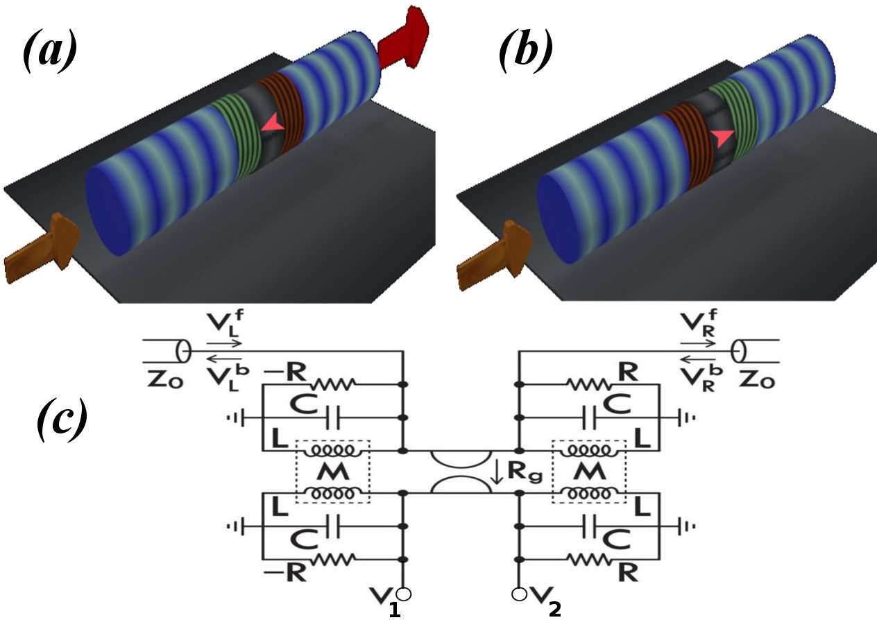
In this Letter, we propose a physical setting (see Fig. 1) which acts as a perfect one-way valve i.e. a channel along which waves propagate in only a single direction, with zero reflection, a perfect impedance matching isolator. This is achieved by employing an interface between a gyrotropic element and two active constituents, one with gain and another one with a balanced amount of loss. In contrast to standard parity-time ()-symmetric systems, first proposed in the framework of optics by Christodoulides and colleagues Makris , our structure shows a new type of generalized -symmetry which allows for non-reciprocal transport. Furthermore, an exchange of the active elements together with an inversion of the gyrotropy leads to unidirectional absorption where an incoming wave entering the structure from one side is completely annihilated. These features can be observed over a broad range of frequencies when 1D chains of such elements are considered. Finally, the presence of imperfections results in destructive interferences that are sensitive to the direction of propagation, a phenomenon refer to as asymmetric Anderson localization. Below we present realizations of such multi-functional architectures, both in the frame of photonics and electronics circuitry (EC). The later framework has been proven recently SLZEK11 extremely useful for the investigation of the transport properties of -symmetric systems.
The photonic structures that we consider consist of a central magneto-optics layer sandwiched between two equally balanced gain and loss birefringent layers which allow for coupling between the polarizations (see Fig. 1a). The role of the magnetic element is to induce magnetic non-reciprocity which is associated with the breaking of time reversal symmetry. Breaking time-reversal symmetry is not sufficient to obtain non-reciprocal transport - the theory of magnetic groups shows that the absence of space inversion symmetries is also required. This is achieved with the use of the two active birefringent layers RLKKKV12 and an anisotropic Bragg mirror which has missalignment with the active layers; therefore it does not allow for coupling between the two polarization channels.
The equivalent EC (Fig. 1b) comprised of two pairs of mutually inductive, , coupled oscillators, one with amplification (left column of Fig. 1b) and the other with equivalent attenuation (right column of Fig. 1b). The loss imposed on the right half of the structure is a standard resistor . Gain imposed on the left half of the EC, symbolized by -, is implemented with a negative impedance converter (NIC). The NIC gain is trimmed to oppositely match the value of R used on the loss side, setting the gain and loss parameter . The uncoupled frequency of each resonator is . The pairs are coupled with each other via a gyrator T48 . This element immitates the role of the magnetic layer used in the photonic set-up. The gyrator is a lossless two-port network component with an antisymmetric impedance matrix connecting the input and output voltages and currents associated with ports and as
| (1) |
where and is a dimensionless conductance. Eq. (1) is invariant under a generalized time reversal operator which performs a combined time-inversion () together with a transposition of . The anti-linear operator is equivalent to the transformation . Despite the fact that a gyrator breaks the time-reversal symmetry, it does not alone leads to non-reciprocal transport (in a similar manner that a magnetic layer is not sufficient to create asymmetric transport in the optics framework).
Finally, the two (upper/lower) propagation channels that are supported by the EC structure of Fig. 1b imitate the polarization channels of the photonic set-up. In the latter case, the BG act as a polarization filter for incident waves with frequencies chosen from the pseudo-gaps. These pseudo-gaps are a consequence of the anisotropic refraction index along the and polarization channels. The analogous effect can be achieved in the EC case by coupling only the upper (or lower) channel to a transmission line (TL) with impedance .
Although below we exploit the simplicity of the electronic (lump) circuitry framework in order to guide the physical intuition and derive theoretical expressions for the transport characteristics of these structures, we will always validate our results in the realm of photonic circuitry via detail simulations.
At any point along a TL, the current and voltage determine the amplitudes of the right and left traveling wave components. The forward and backward wave amplitudes, and and the voltage and current at the left (L) or right (R) TL-EC contacts satisfy the continuity relations
| (2) |
Note that with this convention, a positive lead current flows out of the right circuit, but into the left circuit, and that the reflection amplitudes for left or right incident waves are defined as and respectively.
Application of the first and second Kirchoff’s laws at the TL-EC contacts allow us to find the current/voltage wave amplitudes at the left and right contact. We get
| (3) |
where , is the voltage at the lower channels (see Fig. 1a), is the gain/loss parameter, and is the dimensionless TL impedance. Here, the dimensionless wave frequency is in units of . Equations (3) are invariant under a combined parity (i.e. ) and (i.e. ) transformation (we recall that the time-reversal is equivalent to conjugation).
For the EC structure of Fig. 1b, the transmission and reflection amplitudes in terms of the gyrotropic and dissipative conductances and are derived using Eqs. (3)
| (4) |
where the functions and are given at the supplement and satisfy the symmetry relations , and . Consequently, these symmetry relations can be translated to the following relations for the transmission and reflection amplitudes for any frequency
| (5) |
The corresponding left (L) and right (R) transmitance and reflectance are then defined as and respectively.
The ratio between the left and right transmission takes the simple form
| (6) |
which establishes the nonreciprocal nature of -symmetric transport. Note that results in reciprocal transport irrespective of the value of . The same conclusion is reached for , corresponding to standard -symmetric structures. Therefore we conclude that non-reciprocal transport is achieved due to the the interplay between gain/loss elements (i.e. ) together with gyrotropic constituent .
Furthermore one can show that the left (right) transmission and reflection amplitudes satisfy the relations
| (7) |
which again implies that in general transport is non-reciprocal. In the photonic case the transmission and reflection amplitutes becomes matrices. In fact, Eqs. (7) are consequences of generalized unitarity relations satisfied by the scattering matrix RLKKKV12 ; Sc12 .
In Fig. 2a we report representative cases of the reflected and transmitted signals for a left and right incident waves. A striking feature of these plots is the fact that at specific frequencies the transmittance from one side can become zero, while from the other side is high. At these specific values of (), the EC acts as a perfect isolator. For example, the requirement for zero transmittance for a left incoming wave leads to
| (8) |
while the frequency where is simply . At these frequencies Eq. (7) collapses to the relation , i.e. the reflection from one side is enchanced while from the other side is suppressed.
Depending on the reflectance properties at , we now distinguish two different types of perfect isolation: (a) In the first case, the reflection of an incident wave entering the sample in the direction that we have non-zero transmitivity, is zero. For example, the transport characteristics of a right incident wave would be and while, the same wave entering the circuit from the opposite (left) direction results in and . We refer to this case as impedance-matched isolator (IMI) as the transmitted signal does not experience any reflection at the TL-circuit interface. (b) In the second case the signal is completely absorbed (i.e. neither transmitted nor reflected) from one direction, while it is transmitted (and partially reflected) from the other. We refer to this case as unidirectional absorber (UA). An example of such modes associated with the former case is marked with a (red) circle in Fig. 2a while a representative mode for the latter case is indicated with a (blue) triangle in Fig. 2a. Based on the symmetry relations of Eq. (5) we deduce that a change from a UA to a IMI behavior occurs by simply performing the transformation . Instead a simultaneous exchange of gain/loss elements i.e. , will result in the same behavior (UA or IMI) but for an incident wave entering the structure from the opposite direction.
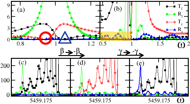
In Fig. 2b we report the left/right reflectances and transmitances, for a 1D network consisting of identical EC units. We observe that a perfect isolation is now extended over a broad-band frequency window (see highlighted area). A simple theoretical understanding for the isolation action can be achieved by realizing that in this case where is the transfer matrix of each EC unit and is the transfer matrix associated with the total array. A Taylor expansion of the right hand side around a frequency of an individual unidirectional unit requires knowledge of the th order derivatives at i.e. for . These vanishing derivatives appreciably flatten the transmitance at a neighborhood around , effectively creating perfect isolation for a broad-band frequency domain, in agreement with the simulations shown in Fig. 2b. Moreover an IMI behavior is evident from our data. We have also checked that the previous expectations associated with the -symmetries are confirmed in the case of 1D chains as well. The same behavior is also present for the equivalent periodic photonic crystal consisting of basic unidirectional units as can be seen from Figs. 2c-e.
Finally, we investigate the effect of imperfections along 1D chains with local -symmetry. We assume that in the case of ECs the disorder is introduced on the capacitances which are independently distributed around a typical capacitance with a uniform probability distribution in the interval . In the absence of any gain/loss elements, such 1D chains exhibit the phenomenon of Anderson localization. This phenomenon was predicted fifty years ago in the framework of quantum (electronic) waves by Anderson A58 and its existence has been confirmed in recent years by experiments with classical CSG00 ; HSPST08 ; LAPSMCS08 ; SBFS07 and matter waves A08 ; Ignuscio .
Formally, the Anderson localization can be quantified via the so-called localization length which is defined as
| (9) |
where denotes an ensemble average over disorder realizations. In reciprocal disordered systems, the localization length satisfies the relations . We find instead that our set-up allows for asymmetric localization with . This is demonstrated in the upper inset of Fig. 3 where we report the scaling behavior of for an 1D chain consisting of disordered EC units, each respecting locally a -symmetry. Straightforward algebra leads to the following expression for the difference between the two localization lengths
| (10) |
where , and . In the main panel of Fig. 3 we compare the theoretical predictions of Eq. (10) together with the numerical results from the transfer matrix simulations of the disordered chain.
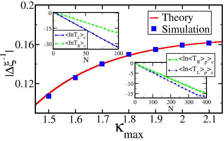
The asymmetric localization can be also observed in the equivalent photonic crystal consisting of random -symmetric units similar to the one shown in Fig. 1a. The disorder was introduced in the real part of the permitivity of the active elements in such a way that in all cases the individual units were preserving a local -symmetry. The numerical evaluation of is performed using transfer matrices and the results are shown in the lower inset of Fig. 3. In this case, an additional average over different polarizations was performed in order to guarantee that the phenomenon is polarization independent.
In conclusion, we have demonstrated both theoretically and numerically the dual behavior of -symmetric (photonic and electronic) circuits as perfect-impedance matched isolators or unidirectional absorbers. One-dimensional arrays consisting of such -symmetric units can demonstrate these dual properties for a broad-band frequency window. Finally, we have shown that disordered 1D arrays with local -symmetry, show asymmetric (left/right) interference effects that can lead to asymmetric Anderson localization. It will be interesting to exploit the simplicity of ECs in order to investigate experimentally such phenomena and extend the analysis towards directional chaos and localization where a localization-delocalization phase transition was predicted even for 1D arrays HN96 ; E97 ; S98 . We expect that fabricating such multi-functional components in the frame of electronic complementary metal oxide semiconductor (CMOS) circuits volakis and the frame of Indium Phosphide Photonic (InP) monolithic Integrated Circuits bowers will occur the years to come and the findings of the optics community will pollinate the silicon photonics and InP communities.
Acknowledgements The work identified in this paper was sponsored by the Air Force Research Laboratory (AFRL/RY), through the Advanced Materials, Manufacturing and Testing Information Analysis Center (AMMTIAC) contract with Alion Science and Technology. Partial support from AFOSR grants No. FA 9550-10-1-0433 and LRIR 09RY04COR are also acknowledged.
References
- (1) Ch. Kittel, Introduction to Solid State Physics, Wiley (2005).
- (2) B. E. A. Saleh and M. C. Teich, Fundamentals of Photonics (Wiley, New York, 1991); A. Yariv, Optical Electronics in Modern Communications (Oxford University Press, 1997).
- (3) W. Wan, Y. Chong, L. Ge, A. D. Stone, and H. Cao, Science 331, 889 (2011).
- (4) S. Lepri, G. Casati, Phys. Rev. Lett. 106, 164101 (2011)
- (5) M. Terraneo, M. Peyrard, G. Casati, Phys. Rev. Lett. 88, 094302 (2002); D. Segal, A. Nitzan, ibid. 94, 034301 (2005); C. W. Chang et al., Science 314 1121 (2006).
- (6) V. F. Nesterenko et al., Phys. Rev. Lett. 95, 158702 (2005).
- (7) K. Gallo et al., Appl. Phys. Lett. 79, 314 (2001).
- (8) M. Scalora et al., J. Appl. Phys. 76, 2023 (1994); M. D. Tocci et al., Appl. Phys. Lett. 66, 2324 (1995).
- (9) F. Biancalana, J. of Appl. Phys. 104, 093113 (2008).
- (10) K. G. Makris et al., Phys. Rev. Lett. 100, 103904 (2008); C. E. Rüter et al., Nat. Phys. 6, 192 (2010); A. Regensburger et al., Nature 488, 167 (2012)
- (11) J. Schindler et al., Phys. Rev. A 84, 040101(R) (2011); Z. Lin et al., Phys. Rev. A 85, 050101(R) (2012); H. Ramezani et al., Phys. Rev. A 85, 062122 (2012); J. Schindler et al., J. Phys. A: Math. Theor. 45 444029 (2012).
- (12) H. Ramezani et al., Optics Express 20, 26200 (2012).
- (13) B. Tellegen, Philips Research Reports 3, 81 (1948); A. Figotin, I. Vitebsky, SIAM J. Appl. Math. 61, 2008 (2001).
- (14) H. Schomerus, arXiv:1207.1454 (Phil trans A in press)
- (15) A. Mostafazadeh, J. Math. Phys. 44, 974 (2003).
- (16) P. Anderson, Phys. Rev. 109, 1492 (1958).
- (17) A.A. Chabanov, M. Stoytchev, & A.Z. Genack, Nature 404, 850 (2000); J.D. Bodyfelt et al., Phys. Rev. Lett. 102, 253901 (2009).
- (18) H. Hu et al., Nature 4, 945 (2008).
- (19) Y. Lahini et al., Phys. Rev. Lett 100, 013906 (2008).
- (20) T. Schwartz et al., Nature 446, 52 (2007).
- (21) A. Aspect et al., Nature 453, 891 (2008).
- (22) G. Roati et al., Nature 453, 895 (2008).
- (23) N. Hatano, D. R. Nelson, Phys. Rev. Lett. 77, 570 (1996).
- (24) K. B. Efetov, Phys. Rev. Lett. 79, 1797 (1997); K. B. Efetov Phys. Rev. B 56, 9630 (1997)
- (25) P. G. Silvestrov, Phys. Rev. B 58, R10111 (1998).
- (26) S. Koulouridis, J. L. Volakis, Antennas and Prop. Soc. Int. Symposium, IEEE APSURSI (2009)
- (27) D. Dai, J. Bauters and J. E Bowers, Light: Science & Applications 1 (2012)
Supplementary Material for Transmissions/Reflections amplitudes [Eq. (4)]
The transmissions and reflections amplitudes can be expressed using the following three functions , , and which are defined for any frequency as
where and are real functions such that
To express these three functions the following shorthand notations are used:
Using the above expressions we get after straightforward algebra,