Predicted septuple-atomic-layer Janus (M=Mo and W) monolayers with Rashba spin splitting and high electron carrier mobilities
Abstract
Janus two-dimensional (2D) materials have attracted much attention due to possessing unique properties caused by their out-of-plane asymmetry, which have been achieved in many 2D families. In this work, the Janus monolayers are predicted in new 2D family by means of first-principles calculations, and of which have been synthesized in experiment(\textcolor[rgb]0.00,0.00,1.00Science 369, 670-674 (2020)). The predicted (M=Mo and W) monolayers exhibit dynamic, thermodynamical and mechanical stability, and they are indirect band-gap semiconductors. The inclusion of spin-orbit coupling (SOC) gives rise to the Rashba-type spin splitting, which is observed in the valence bands, being different from common conduction bands. Calculated results show valley polarization at the edge of the conduction bands due to SOC together with inversion symmetry breaking. It is found that (M=Mo and W) monolayers have high electron mobilities. Both in-plane and much weak out-of-plane piezoelectric polarizations can be observed, when a uniaxial strain in the basal plane is applied. The values of piezoelectric strain coefficient of the Janus (M=Mo and W) monolayers fall between those of the (M=Mo and W) and (M=Mo and W) monolayers, as expected. It is proved that strain can tune the positions of valence band maximum (VBM) and conduction band minimum (CBM), and enhance the the strength of conduction bands convergence caused by compressive strain. It is also found that tensile biaxial strain can enhance of (M=Mo and W) monolayers, and the compressive strain can improve the (absolute values). Our predicted (M=Mo and W) monolayers as derivatives of 2D family enrich Janus 2D materials, and can motivate related experimental works.
pacs:
71.20.-b, 77.65.-j, 72.15.Jf, 78.67.-n Email:sandongyuwang@163.comI Introduction
The exploration of grapheneq6 enormously promotes the search for new 2D materials both in experiment and in theory, which have potential applications in the field of optoelectronics, spintronics, valleytronics and energy conversion and storage. Numerous 2D materials have been found, including transition metal chalcogenides (TMDs), group-VA, group IV-VI, group-IV, transition metal carbides/nitrides (Mxenes), , and monolayersq7 ; q8 ; q9 ; p1 ; q6-1 ; q6-1-1 ; q6-1-2 ; q6-1-3 ; q6-1-4 ; q6-2 ; q10 ; q11 . The unique crystal structure together with strong SOC in monolayer TMDs demonstrates coupled spin-valley physicsq6-5 , and the buckled honeycomb structure plus strong SOC can give rise to quantum spin Hall (QSH) and quantum anomalous Hall (QAH) effects in a particular type of 2D Xeneq6-5-1 ; q6-5-2 . An emerging class of 2D materials (Janus 2D materials) have currently attracted increasing attention due to unique crystal structures, which lack the reflection symmetry with respect to the central atomic layerq6-5-3 . In these 2D Janus materials, the strong Rashba spin splitting, second harmonic generation response and out-of-plane piezoelectric polarizations can be achievedq6-5-3 . Many Janus 2D materials have been proposed, such as Janus graphene, asymmetrically functionalizing silicene monolayer, Janus TMDs, Janus transition-metal oxides, PtSSe, TiXY (X/Y=S, Se and Te), VSSe, SnSSe and Janus group-III monochalcogenide (M=Ga, In; X/Y=S, Se, Te)zs-1 ; zs-2 ; zs-3 ; zs-4 ; zs-5 ; zs-6 ; zs-7 ; zs-8 ; zs-9 . Recently, Janus monolayer MoSSe has been successfully achieved by different experimental strategiesp1 ; p1-new with additional out-of-plane piezoelectric coefficientp2 ; p2-new .


Recently, by chemical vapor deposition (CVD), the septuple-atomic-layer 2D and have been synthesizedmsn , which opens up a new 2D material family. The density functional theory (DFT) calculations predict many similar 2D materials with a general formula of , where M represents an early transition metal (W, V, Nb, Ta, Ti, Zr, Hf, or Cr), A is Si or Ge, and Z stands for N, P, or Asmsn . In quick succession, by intercalating -type monolayer into InSe-type monolayer, twelve kinds of 2D family are proposed with and (=1 to 6) phases with diverse properties from semiconductor to topological insulator to Ising superconductorm20 . Intrinsic piezoelectricity in monolayer (M=Mo, W, Cr, Ti, Zr and Hf) has been predicted by the first-principle calculationsm21 . It is also predicted that the strain can effectively tune the electronic properties of monolayer, and it undergoes ferromagnetic metal (FMM) to spin-gapless semiconductor (SGS) to ferromagnetic semiconductor (FMS) to SGS to ferromagnetic half-metal (FMHM) with increasing strainm22 . The valley-dependent properties of monolayer , and have been studied by the DFT calculationsm23 ; m24 .
It’s a natural idea to achieve Janus 2D materials in the new septuple-atomic-layer 2D family. In this work, inspiring from the already synthesized (M=Mo and W) by introducing Si during CVD growth of (M=Mo and W)msn , we construct the (M=Mo and W) monolayers, which may be achieved by introducing Si and Ge during CVD growth of (M=Mo and W). Their electronic structures, carrier mobilities and piezoelectric properties have been investigated, and show distinct Rashba spin splitting and out-of-plane piezoelectric polarizations compared to (M=Mo and W) monolayersm21 . It is found that the strain can effectively tune the electronic structures and piezoelectric properties of (M=Mo and W) monolayers.
The rest of the paper is organized as follows. In the next section, we shall give our computational details and methods. In the next few sections, we shall present structural stabilities, electronic structures, carrier mobilities and piezoelectric properties of (M=Mo and W) monolayers, along with strain effects on their electronic structures and piezoelectric properties. Finally, we shall give our discussion and conclusions.
| Name | Gap | Gap-SOC | ||
|---|---|---|---|---|
| 2.963 | 1.116 | 1.126 | 0.8 | |
| 2.964 | 1.428 | 1.408 | 4.2 |
II Computational detail
We perform DFT1 calculations for structural relaxation and electronic structures by using the Perdew-Burke-Ernzerhof generalized gradient approximation (PBE-GGA) for the exchange and correlation function, as implemented in the Vienna ab initio simulation package (VASP)pv1 ; pv2 ; pv3 ; pbe . To describe the electron-ion interaction, we use the projector augmented wave (PAW) method. For energy band calculations of (M=Mo and W) monolayers, the SOC is also taken into account. A cutoff energy of 500 eV for the plane wave basis set is used to ensure an accurate DFT calculations. For the convergence of electronic self-consistent calculations, the total energy convergence criterion is set to eV, and the Hellmann-Feynman forces on each atom are less than 0.0001 . A vacuum spacing of more than 32 is adopted to decouple the spurious interaction between the layers.
The coefficients of the elastic stiffness tensor and piezoelectric stress coefficients are calculated by using strain-stress relationship (SSR) and density functional perturbation theory (DFPT) methodpv6 , respectively. The Brillouin zone sampling is done using a Monkhorst-Pack mesh of 16161 for , and 9161 for . The 2D elastic coefficients and piezoelectric stress coefficients have been renormalized by the length of unit cell along z direction (): = and =. The phonon dispersion spectrums are calculated by Phonopy codepv5 with a supercell of 551 using the finite displacement method, and a 331 k-mesh is employed. The kinetic energy cutoff is set to 500 eV. The constant energy contour plots of the spin texture are calculated by the PYPROCAR codepy .


III Structure and stability
The top view and side view of crystal structure of (M=Mo and W) monolayers are shown in Figure 1, and the rhombus primitive cell and the rectangle supercell are shown. The structure of monolayer (M=Mo and W) could be regarded as a layer sandwiched by Si-N and Ge-N bilayers, which can be constructed by replacing the Si/Ge atoms of top SiN/GeN bilayer in / monolayer with Ge/N atoms. If the Si-N or Ge-N bilayers is considered as a whole, the (M=Mo and W) monolayers can be viewed as Janus 2D materials. The symmetry of (M=Mo and W) monolayers (No.156) is lower than that of the / monolayer (No.187) due to the lack of the reflection symmetry with respect to the central M atomic layer. The reduced symmetry can lead to many novel properties, such as Rashba spin splitting and out-of-plane piezoelectric polarizations.
The optimized lattice constants of / is ==2.963/2.964 with GGA, being between the ones of (2.91 )/ (2.91 ) and (3.02 )/ (3.02 )msn ; m20 . The dynamical stability of the (M=Mo and W) monolayers are tested by analyzing the phonon spectra. Their phonon band dispersions calculated along the high-symmetry directions of the Brillouin zone are shown in Figure 2. The 18 optical and 3 acoustical phonon branches as a total of 21 branches due to 7 atoms per cell are observed. It is clearly seen that the outlines of phonon band dispersions between and are very similar. It is noted that the out-of-plane acoustic (ZA) branch corresponding to the out-of-plane vibrations deviates from linearity, which agrees well with the conclusion that the ZA phonon branch should have quadratic dispersion, when the sheet is free of stressr1 ; r2 . All phonon frequencies of the (M=Mo and W) monolayers are positive, which confirms their dynamical stability, and they can exist as free-standing 2D materials.

It is important to check the mechanical stability of the (M=Mo and W) monolayers by elastic constants . The hexagonal symmetry leads to two independent elastic constants and for (M=Mo and W) monolayers. The calculated ==486.71 /508.27 and =144.14 /147.21 for / monolayer. For hexagonal symmetry, the mechanical stability of a material should satisfy the Born criteria of mechanical stabilityela :
| (1) |
where the =(-)/2. The calculated confirm the mechanical stability of (M=Mo and W) monolayers. The Young’s modulus can be calculated on the basis of the elastic constantsela1 :
| (2) |
where . It is worth noting that (M=Mo and W) monolayers are mechanically isotropic. The calculated is 444.02 /465.63 for / monolayer, which are larger than ones of most 2D materialsela2 ; ela3 ; ela4 ; ela5 , indicating that these monolayers are rigid. The Poisson’s ratio is also isotropic, and can be attained by:
| (3) |
The calculated is 0.296/0.290 for / monolayer.
To verify the stability of the (M=Mo and W) monolayers at room temperature, ab initio molecular dynamics (AIMD) simulations are carried out with a supercell of size 441 for more than 3000 fs with a time step of 1 fs. The total energy fluctuations of (M=Mo and W) monolayers as a function of simulation time together with crystal structures at 300 K after the simulation for 3 ps are shown in FIG.1 of ESI. Calculated results show no obvious structural disruption with the total energy fluctuates being small after 3 ps at 300 K, which proves that (M=Mo and W) monolayers are thermodynamically stable.
The dynamical, thermal and mechanical stability of the (M=Mo and W) monolayers are proved by phonon calculations, AIMD and elastic constants, suggesting the possible synthesis of these monolayers. By introducing Si during CVD growth of (M=Mo and W), monolayer (M=Mo and W) have been synthesized in experimentmsn . If the Si and Ge are simultaneously introduced during CVD growth of (M=Mo and W) to passivate its surface, it is possible to achieve (M=Mo and W) monolayers.

IV Electronic structure
Due to containing transition metal in (M=Mo and W) monolayers, the SOC is also taken into account. In fact, it has been proved that the SOC has important effects on electronic structures of monolayer (M=Mo and W), which exhibit rich spin-valley physicsm20 ; m23 ; m24 . Therefore, the SOC is considered for electronic structure calculations of (M=Mo and W) monolayers, and their energy band structures with both GGA and GGA+SOC are plotted in Figure 3. Both GGA and GGA+SOC results show that (M=Mo and W) monolayers are indirect gap semiconductors with the CBM at K point. To accurately determine VBM, the enlarged views of the valence bands near the Fermi level for (M=Mo and W) monolayers using GGA and GGA+SOC are plotted in Figure 4. For GGA results, the valence bands of around the point near the Fermi level are flat with the error less than 1 meV, and the VBM of deviates slightly the point. Due to the intrinsic out-of-plane electric field induced by the mirror asymmetry, the Rashba-type spin splitting around the point is observed, when the SOC is included. This gives rise to the deviation of VBM of (M=Mo and W) monolayers with GGA+SOC. It is found that the gap values of (M=Mo and W) monolayers between GGA and GGA+SOC are very close, and the related data are summarized in Table 1.
From FIG.2 of ESI, the Zeeman-type spin splitting around K/K1 point (the degenerate K and K1 valleys ) in the valence bands near the Fermi level is observed due to SOC together with inversion symmetry breaking. The respective time-reversal symmetry requires that the spin splitting must be opposite at the two distinct valleys, which can be observed from FIG.2 of ESI. Moreover, due to the existence of the horizontal mirror, they are fully spin-polarized in the out-of-plane direction (only component), which is confirmed by our calculated results with FIG.2 of ESI being only component. (M=Mo and W) monolayers have conduction band valleys at K and K1. Although the VBM is not at the K/K1, the valleys are still well defined and not far in energy. The similar results can be observed in monolayer , and m23 ; m24 .
The constant energy 2D contour plots of spin texture calculated in a plane centered at the point are shown in Figure 5. The Rashba-type spin splitting of spin-up (red) and spin-down (blue) electronic bands can be distinctly observed. The 2D Rashba spin splitting of valence bands gives rise to the concentric spin-texture circles with clockwise and counterclockwise rotating spin directions, respectively. The concentric spin-texture circles are due to the pure 2D Rashba spin splitting in the valence bands. It is found that only in-plane and spin components are present in the Rashba spin split bands, without the presence of any out-of-plane component, which is also proved from FIG.2 of ESI. The strength of the Rashba effect can be measured by three key parameters: the Rashba energy (), the Rashba momentum (), and the Rashba constant (), and they can be connected by =2/. The and are shown in Figure 4. We find that , and of / monolayer are 0.8/4.2 meV, 0.048/0.076 , and 0.033/0.111 eV.
V Carrier mobility and Piezoelectric properties
The carrier mobilities () of (M=Mo and W) monolayers are calculated by the deformation potential (DP) theory proposed by Bardeen and Shockleydp , which is defined as:
| (4) |
where , is temperature and the effective mass in the transport direction, and is the average effective mass. The elastic modulus can be attained from . In addition, is the DP constant defined by , where is the energy shift of the band edge of CBM or VBM with respect to the vacuum level, and with applying uniaxial strain.
| Carrier type | () | (eV) | () | |||
|---|---|---|---|---|---|---|
| Electrons | x | 444.02 | 0.41 | -3.37 | 5205.14 | |
| y | 444.02 | 0.38 | -3.13 | 6573.25 | ||
| Holes | x | 444.02 | -10.66 | 3.56 | 6.56 | |
| y | 444.02 | -10.67 | 3.39 | 7.22 | ||
| Electrons | x | 465.63 | 0.30 | -4.06 | 7046.80 | |
| y | 465.63 | 0.28 | -3.75 | 8767.94 | ||
| Holes | x | 465.63 | -8.73 | 4.17 | 19.45 | |
| y | 465.63 | -1.29 | 3.83 | 155.43 |

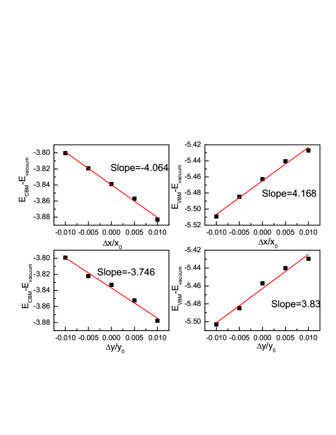
According to DP theory, we calculate the carrier mobilities of (M=Mo and W) monolayers in both zigzag and armchair directions with armchair and zigzag being defined as x and y directions in Figure 1. The calculated effective masses for electrons and holes of (M=Mo and W) monolayers with GGA+SOC are shown in Table 2. It is worth noting that the SOC has very important effects on the effective masses for holes due to different energy structures between GGA and GGA+SOC in Figure 4. The band energies of the VBM and CBM with respect to the vacuum energy as a function of and are plotted in Figure 6 for monolayer, and FIG.3 of ESI for monolayer. By linearly fitting these energy values, the DP constant can be attained. The carrier mobilities of (M=Mo and W) monolayers for the electrons and holes along x and y directions are attained on the basis of the calculated , and . The related data are summarized in Table 2. The very strong anisotropy of predicted carrier mobilities between electrons and holes is observed, and the electron carrier mobilities of (M=Mo and W) monolayer are very higher than those of holes. The electron carrier mobilities of () along x and y directions are up to 5205 (7047 ) and 6573 (8768 ).
Next, we investigate the piezoelectric properties of (M=Mo and W) monolayers. Performing symmetry analysis, due to a point-group symmetry, the piezoelectric stress and strain tensors, and elastic tensor can be reduced intoela2 :
| (5) |
| (6) |
| (7) |
Here, the independent and are derived by :
| (8) |
| Name | ||||
|---|---|---|---|---|
| 4.395 | 1.144 | - | - | |
| 5.116 | 1.494 | -0.087 | -0.014 | |
| 5.621 | 1.846 | - | - | |
| 3.138 | 0.778 | - | - | |
| 3.790 | 1.050 | 0.073 | 0.011 | |
| 4.218 | 1.306 | - | - |
For , the orthorhombic supercell of (M=Mo and W) monolayers (in Figure 1) is adopted, and the calculated and are summarized in Table 3, along with ones of (M=Mo and W; A=Si and Ge) monolayer. With respect to the central M atomic plane, the (M=Mo and W; A=Si and Ge) monolayer possess a reflection symmetry due to symmetry, which leads to that they have only in-plane piezoelectricity. For (M=Mo and W) monolayers, the difference in atomic sizes and electronegativities of the second and sixth layer atoms breaks the reflection symmetry along the vertical direction, giving rise to a low degree of symmetry. Therefore, both in-plane and vertical piezoelectricity are allowed in (M=Mo and W) monolayers, when they are subject to a uniaxial in-plane strain. It is clearly seen that both and increase with increasing atomic mass from (M=Mo and W) to (M=Mo and W) to (M=Mo and W). It is found that the and (A=Si and Ge) monolayers have higher / values than and (A=Si and Ge) monolayers. For a given metal element M, the monolayers containing heavier column IV element have larger / values. More significantly, the (M=Mo and W) monolayers possess the vertical piezoelectric effect, which can be described by /. However, they are smaller by two orders of magnitude compared to /. Similar phenomenon can be observed in Janus MXY (M = Mo or W, X/Y = S, Se, or Te) monolayerela2 .


VI Strain effects
It has been proved that the electronic structures, topological properties, transport and piezoelectric properties of 2D materials can be effectively tuned by strainm12 ; m13 ; m14 ; m15 ; r6 ; r7 ; r8 . Here, we use to examine the effects of biaxial strain on the electronic structures of (M=Mo and W) monolayers, where and are the strained and unstrained lattice constant with 1 (1) being compressive (tensile) strain, The energy band structures of with from 0.90 to 1.10 are plotted in Figure 7, and the related energy band structures are shown in FIG.4 of ESI for . The energy band gaps of (M=Mo and W) monolayers as a function of are shown in Figure 8. It is found that the energy band gap of (M=Mo and W) monolayers firstly increases with increasing , and then decreases. The up-and down trend of gap can also be observed in many 2D materials, like Janus TMD monolayersq5 and GeSq5-11 . The compressive strain can make conduction band extrema (CBE) of monolayer converge, especially for 0.96 and 0.98 strains. The conduction bands convergence is in favour of n-type Seebeck coefficient. The compressive strain can make K point become VBM, which is very useful for manipulating valley pseudospin. The compressive strain produces another effect that the CBM changes from K point to one point along K- line. Similar strain effects on electronic structures of can be found. It is noted that (M=Mo and W) monolayers in considered strain range are all semiconductors, which is useful for their piezoelectric application with strain.
The piezoelectric strain coefficients of (M=Mo and W) monolayers are very small, and strain engineering may be an effective way to enhance their piezoelectric properties. Next, we consider the strain effects on piezoelectric properties of (M=Mo and W) monolayers. The elastic constants (, , - and +), piezoelectric stress coefficients ( and along the ionic and electronic contributions), and piezoelectric strain coefficients ( and ) of monolayer as a function of biaxial strain are plotted in Figure 9, Figure 10 and Figure 11, respectively. For , these are shown in FIG.5, FIG.6 and FIG.7 of ESI, respectively. With strain from 0.90 to 1.10, the increases due to decreased - and enhanced based on Equation 8. At 10% strain, the of () is 7.282 pm/V (8.081 pm/V), which is about seven times (five times) as large as unstrained one of 1.050 pm/V (1.494 pm/V). It is found that both ionic and electronic parts have positive contribution to with increasing tensile strain. Similar biaxial strain-enhanced can be observed in monolayer , g- and m21 ; gsd . It is observed that the compressive strain can improve the (absolute value) of (M=Mo and W) monolayers due to enhanced (absolute value), and the can be improved to 0.082 pm/V (-0.086 pm/V) for () at 0.90 strain. Finally, it is found that the (M=Mo and W) monolayers are mechanically stable in the considered strain range, based on calculated elastic constants satisfying the mechanical stability criteria.
VII Discussions and Conclusion
The (M = Mo, W) monolayers have been recently synthesized, which are grown by passivating the surface dangling bonds of (M = Mo, W) layer with Si-N tetrahedra when introducing elemental Simsn . Thus, it is possible to achieve Janus (M=Mo and W) monolayers by simultaneously introducing Si and Ge elements during CVD growth of nonlayered (M = Mo, W) to passivate its surface. Compared to (M = Mo, W) monolayers, the most important difference is that Janus (M=Mo and W) monolayers have out-of-plane piezoelectric polarization and Rashba effect due to their out-of-plane asymmetry. Although their out-of-plane piezoelectric polarization and Rashba effect are very weak, our works open a new avenue to achieve Janus materials in the new 2D family.
In summary, we investigate the electronic structures, carrier mobilities, piezoelectric properties of (M=Mo and W) monolayers by the reliable first-principle calculations. They are found to exhibit mechanical, thermodynamical and dynamic stability, and high experimental feasibility.
It is found that (M=Mo and W) monolayers are indirect gap semiconductors. When the SOC is considered, the Rashba effect can be observed in the valence bands of (M=Mo and W) monolayers. Their electron mobilities are very high due to very light electron effective masses. The of (M=Mo and W) monolayers can be induced by a
uniaxial strain in the basal plane, similar to (M = Mo, W) monolayers. In addition to this, a vertical piezoelectric polarization can be produced upon application of uniaxial or biaxial strains due to the lack of reflection symmetry
with respect to M atomic layer. Calculated results show that compressive strain can change the positions of CBM and VBM of (M=Mo and W) monolayers, and tune the strength of conduction bands convergence. It is also found that biaxial strain can enhance
[ (absolute values)] of (M=Mo and W) monolayers by tensile [compressive] strain.
Our works will stimulate further experimental studies to achieve (M=Mo and W) monolayers, and will motivate farther exploration on Janus monolayers in new 2D family.
Conflicts of interest
There are no conflicts to declare.
Acknowledgements.
This work is supported by the Natural Science Foundation of Shaanxi Provincial Department of Education (19JK0809). We are grateful to the Advanced Analysis and Computation Center of China University of Mining and Technology (CUMT) for the award of CPU hours and WIEN2k/VASP software to accomplish this work.References
- (1) K. S. Novoselov et al., Science 306, 666 (2004).
- (2) J. P. Ji, X. F. Song, J. Z. Liu et al., Nat. Commun. 7, 13352 (2016).
- (3) S. Balendhran, S. Walia, H. Nili, S. Sriram and M.Bhaskaran, small 11, 640 (2015).
- (4) S. L. Zhang M. Q. Xie, F. Y. Li, Z. Yan, Y. F. Li, E. J. Kan, W. Liu, Z. F. Chen, H. B. Zeng, Angew. Chem. 128, 1698 (2016).
- (5) A. Y. Lu, H. Y. Zhu, J. Xiao et al., Nature Nanotechnology 12, 744 (2017).
- (6) X. Zhou, Q. Zhang, L. Gan, H. Li and T. Zhai, Adv. Funct. Mater. 26, 4405 (2016).
- (7) C. Gong, L. Li, Z. Li, H. Ji, A. Stern, Y. Xia, T. Cao, W. Bao, C. Wang, Y. Wang, Z. Q. Qiu, R. J. Cava, S. G. Louie, J. Xia and X. Zhang, Nature 546, 265 (2017).
- (8) X. M. Wu, Y. L. Feng, S. Li, B. Q. Zhang and G. Y. Gao, J. Phys. Chem. C 124, 16127 (2020).
- (9) X. Jiang, S. Liu, W. Liang, S. Luo, Z. He, Y. Ge, H. Wang, R. Cao, F. Zhang and Q. Wen, Laser Photonics Rev. 12, 1700229 (2018).
- (10) C. Xing, S. Chen, X. Liang, Q. Liu, M. Qu, Q. Zou, J. Li, H. Tan, L. Liu and D. Fan, ACS Appl. Mater. Interfaces 10, 27631 (2018).
- (11) X. Zhou, L. Gan, W. M. Tian et al., Adv. Mater. 27, 8035 (2015).
- (12) M. Chhowalla, H. S. Shin, G. Eda, L. J. Li, K. P. Loh and H. Zhang, Nature Chemistry 5, 263 (2013).
- (13) R. X. Fei, W. B. Li, J. Li and L. Yang, Appl. Phys. Lett. 107, 173104 (2015).
- (14) T. Cao, G. Wang, W. P. Han et al., Nat. Commun. 3, 887 (2012).
- (15) Y. Deng, Y. Yu, M. Z. Shi, Z. Guo, Z. Xu, J. Wang, X. H. Chen, Y. Zhang, Science 367, 895 (2020).
- (16) J. Li, Y. Li, S. Du, Z. Wang, B. L. Gu, S. C. Zhang, K. He, W. Duan and Y. Xu, Sci. Adv. 5, eaaw5685 (2019).
- (17) L. Zhang, Z. J. F. Yang, T. Gong, R. K. Pan, H. D. Wang, Z. N. Guo, H. Zhang and X. Fu, J. Mater. Chem. A 8, 8813 (2020).
- (18) G. B. R. Singh, Phys. Rev. B 84, 155427 (2011).
- (19) Y. Guo, S. Zhou, Y. Bai and J. Zhao, Appl. Phys. Lett. 110, 163102 (2017).
- (20) M. Sun, Q. Ren, S. Wang, J. Yu and W. Tang, J. Phys. D: Appl. Phys. 49, 445305 (2016).
- (21) Y. C. Cheng, Z. Y. Zhu, M. Tahir and U. Schwingenschlogl, Europhys. Lett. 102, 57001 (2013).
- (22) Y. D. Guo, H. B. Zhang, H. L. Zeng, H. X. Da, X. H. Yan, W. Y. Liu and X. Y. Mou, Phys. Chem. Chem. Phys. 20, 21113 (2018).
- (23) R. Peng, Y. Ma, B. Huang and Y. Dai, J. Mater. Chem. A, 7, 603 (2019).
- (24) A. Mogulkoc, Y. Mogulkoc, S. Jahangirov and E. Durgun, J. Phys. Chem. C 123, 29922 (2019).
- (25) C. Zhang, Y. Nie, S. Sanvito and A. Du, Nano Lett. 19, 1366 (2019).
- (26) S. D. Guo, X. S. Guo, R. Y. Han and Y. Deng, Phys. Chem. Chem. Phys. 21, 24620 (2019).
- (27) J. Zhang, S. Jia, I. Kholmanov et al., ACS Nano 118, 8192 (2017).
- (28) L. Dong, J. Lou and V. B. Shenoy, ACS Nano 11, 8242 (2017).
- (29) M. Yagmurcukardes, C. Sevik and F. M. Peeters, Phys. Rev. B 100, 045415 (2019).
- (30) Y. L. Hong, Z. B. Liu, L. Wang T. Y. Zhou, W. Ma, C. Xu, S. Feng, L. Chen, M. L. Chen, D. M. Sun, X. Q. Chen, H. M. Cheng and W. C. Ren, Science 369, 670 (2020).
- (31) L. Wang, Y. P. Shi, M. F. Liu et al., arXiv:2008.02981 (2020).
- (32) S. D. Guo, Y. T. Zhu, W. Q. Mu and W. C. Ren, EPL (2020).
- (33) S. D. Guo, W. Q. Mu, Y. T. Zhu and X. Q. Chen, Phys. Chem. Chem. Phys. DOI: 10.1039/D0CP05273F (2020).
- (34) S. Li, W. K. Wu, X. L. Feng et al., arXiv:2009.13253 (2020).
- (35) C. Yang, Z. G. Song, X. T. Sun and J. Lu, arXiv:2010.10764 (2020).
- (36) P. Hohenberg and W. Kohn, Phys. Rev. 136, B864 (1964); W. Kohn and L. J. Sham, Phys. Rev. 140, A1133 (1965).
- (37) G. Kresse, J. Non-Cryst. Solids 193, 222 (1995).
- (38) G. Kresse and J. Furthmller, Comput. Mater. Sci. 6, 15 (1996).
- (39) G. Kresse and D. Joubert, Phys. Rev. B 59, 1758 (1999).
- (40) J. P. Perdew, K. Burke and M. Ernzerhof, Phys. Rev. Lett. 77, 3865 (1996). (2006).
- (41) X. Wu, D. Vanderbilt and D. R. Hamann, Phys. Rev. B 72, 035105 (2005).
- (42) A. Togo, F. Oba, and I. Tanaka, Phys. Rev. B 78, 134106 (2008).
- (43) U. Herath, P. Tavadze, X. He, E. Bousquet, S. Singh, F. Munoz and A. H. Romero, Computer Physics Communications 251, 107080 (2020).
- (44) E. Mariani and F. V. Oppen, Phys. Rev. Lett. 100, 076801 (2008).
- (45) J. Carrete , W. Li, L. Lindsay, D. A. Broido, L. J. Gallego and N. Mingo, Mater. Res. Lett. 4, 204 (2016).
- (46) R. C. Andrew, R. E. Mapasha, A. M. Ukpong and N. Chetty, Phys. Rev. B 85, 125428 (2012).
- (47) E. Cadelano, P. L. Palla, S. Giordano and L. Colombo, Phys. Rev. B 82, 235414 (2010).
- (48) L. Dong, J. Lou and V. B. Shenoy, ACS Nano, 11, 8242 (2017).
- (49) M. N. Blonsky, H. L. Zhuang, A. K. Singh and R. G. Hennig, ACS Nano, 9, 9885 (2015).
- (50) R. X. Fei, We. B. Li, J. Li and L. Yang, Appl. Phys. Lett. 107, 173104 (2015).
- (51) K. N. Duerloo, M. T. Ong and E. J. Reed, J. Phys. Chem. Lett. 3, 2871 (2012).
- (52) S. Bruzzone and G. Fiori, Appl. Phys. Lett. 99, 222108 (2011).
- (53) E. Scalise, M. Houssa, G. Pourtois, V. Afanas’ev and A. Stesmans, Nano Res. 5, 43 (2012).
- (54) H. K. Liu, G. Z. Qin, Y. Lin and M. Hu, Nano Lett. 16, 3831 (2016).
- (55) N. Jena, Dimple, S. D. Behere and A. D. Sarkar, J. Phys. Chem. C 121, 9181 (2017).
- (56) Dimple, N. Jena, A. Rawat, R. Ahammed, M. K. Mohanta and A. D. Sarkar, J. Mater. Chem. A 6, 24885 (2018).
- (57) Z. Q. Fan, X. W. Jiang, Z. M. Wei, J. W. Luo and S. S. Li, J. Phys. Chem. C 121, 14373 (2017).
- (58) S. D. Guo, X. S. Guo, Y. Y. Zhang and K. Luo, J. Alloy. Compd. 822, 153577 (2020).
- (59) X. X. Xue, Y. X. Feng, L. Liao, Q. J. Chen, D. Wang, L. M. Tang and K. Chen, J. Phys.: Condens. Matter 30, 125001 (2018).
- (60) S. D. Guo and J. Dong, Semicond. Sci. Tech. 33, 085003 (2018).
- (61) S. L. Zhang, N. Wang, S. G. Liu et al., Nanotechnology 27, 274001 (2016).
- (62) S. D. Guo, W. Q. Mu and Y. T. Zhu, arXiv:2008.05618 (2020).