Probing a Single Nuclear Spin in a Silicon Single Electron Transistor
Abstract
We study single electron transport across a single Bi dopant in a Silicon Nanotransistor to assess how the strong hyperfine coupling with the Bi nuclear spin affects the transport characteristics of the device. In the sequential tunneling regime we find that at, temperatures in the range of , curves reflect the zero field hyperfine splitting as well as its evolution under an applied magnetic field. Our non-equilibrium quantum simulations show that nuclear spins can be partially polarized parallel or antiparallel to the electronic spin just tuning the applied bias.
PACS: 73.23.Hk, 31.30.Gs, 74.55.+v, 75.75.-c
The amazing progress both in the silicon processing technologies and in the miniaturization of silicon based transistors has reached the point where single-dopant transistors have been demonstrated.Sellier et al. (2006); Pierre et al. (2009); Lansbergen et al. (2010); Tan et al. (2010); Golovach et al. (2011); Fuechsle et al. (2012); Tettamanzi et al. (2012) Whereas this progress has been fueled by the development of classical computing architectures, it might also be used for quantum computing. In this regard, the electronic and nuclear spins of single donors in silicon are very promising building blocks for quantum computing.Kane (1998); DiVincenzo et al. (2000); Ladd et al. (2010) Progress along this direction makes it necessary to implement single spin readout schemes both for electronic and nuclear spins. Single electronic spin readout has been demonstrated, both in GaAs quantum dots as well as in P doped Silicon Nanotransistors.Elzerman et al. (2004); Morello et al. (2010)
The readout of the quantum state of a single nuclear spin, much more challenging, has been demonstrated for NV centers in diamond taking advantage of single spin optically detected magnetic resonance afforded by the extraordinary properties of that system.Neumann et al. (2010) Single nuclear spin readout with either opticalFu et al. (2004) or a combined electro-optical techniquesSleiter et al. (2010) has been proposed, but remains to be implemented. Here we explore the electrical readout of a single nuclear spin, more suitable for an indirect band-gap host like Si. A preliminary step is to construct a circuit whose transport is affected by the quantum state of the nuclear spin. There is ample experimental evidence of the mutual influence of many nuclear spins and transport electrons in III-V semiconductor quantum dots in the single electron transport regime.Petta et al. (2008); Reilly et al. (2008); Foletti et al. (2009); Kobayashi et al. (2011) In particular, Kobayashi et al. have reported hysteresis in the upon application of magnetic fields, reflecting the realization of different ensemble of nuclear states coupled to the electronic spin via hyperfine coupling.Kobayashi et al. (2011)
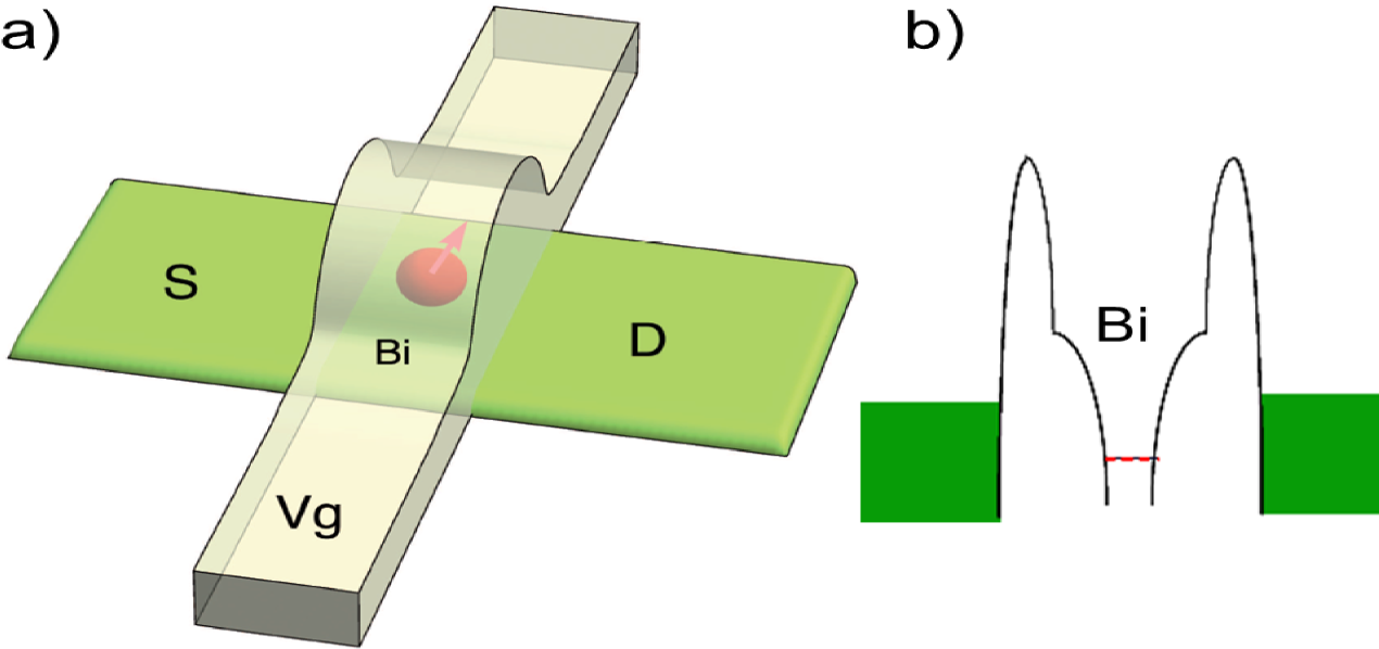
Here we propose a device where a single nuclear spin is probed in single electron transport. We model the single electron transport in a silicon nanotransistor such that, in the active region, transport takes place through a single Bi dopant, see Fig. 1. We show that, at sufficiently low temperatures, the curves of this device probe the hyperfine structure of the dopant level. In turn, the occupations of the nuclear spin states are affected by the transport electrons. Whereas single dopant transistors have been demonstrated for single P, As and B, in Si, Lansbergen et al. (2010); Tan et al. (2010); Morello et al. (2010); Fuechsle et al. (2012) we choose Bi because it has a much larger hyperfine splitting,George et al. (2010); Morley et al. (2010); Mohammady et al. (2010) due to both a larger nuclear spin and a larger hyperfine coupling constant (eV). The zero-field splitting of the Bi donor level is given by and has been observed by electron spin resonanceGeorge et al. (2010); Morley et al. (2010); Mohammady et al. (2010) and in photoluminescence experiments with many dopants.Sekiguchi et al. (2010)
We consider the sequential transport regime, where the occupation of the donor level fluctuates between and . In the state, the nuclear spin interacts only with the external field. In the state, the electron and the nuclear spin are hyperfine coupled. The Hamiltonian that describes both states reads George et al. (2010); Morley et al. (2010); Mohammady et al. (2010); Delgado and Fernández-Rossier (2011)
| (1) |
where is the donor energy level with respect to the Fermi energy, which we take as , and denotes an external gate voltage. We assume that valley degeneracies of the donor level are split-off and neglect the valley degree of freedom. The third term is the hyperfine coupling, and the last two, where and , correspond to the electron and nuclear Zeeman terms, with () the electron (nuclear) g-factors and () the Bohr (nuclear) magneton. In equilibrium, i.e., at zero bias, the occupation of the dopant level depends on the value of the addition energy, which ignoring the Zeeman terms and the tiny correction due to the hyperfine coupling, is given by .
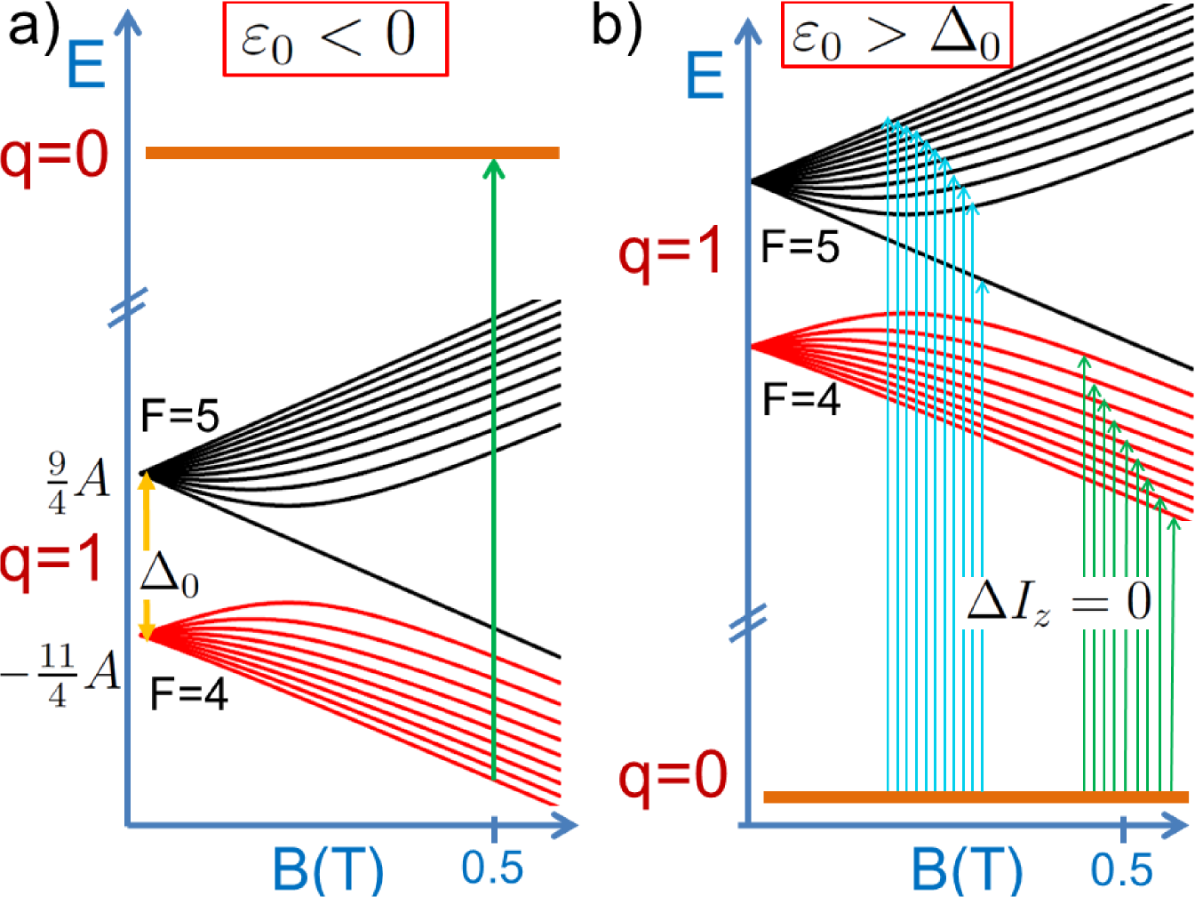
We denote the eigenstates as . Their energies read as . The eigenenergies and eigenvectors of are denoted by and . The zero-field Hamiltonian can be diagonalized in terms of the total angular operator , resulting in two multiplets (F=4, F=5) with energies and , and a zero-field splitting eV. At finite magnetic field, the exact eigenvalues of can also be calculated analytically.Mohammady et al. (2010) The corresponding energy levels are shown in Fig. 2.
The tunneling Hamiltonian between the single Bi dopant level and the source and drain electrodes reads as
| (2) |
where operator annihilates an electron with spin and orbital quantum number , with wave vector and electrode index , while operator annihilates a spin electron in the dopant level. The scattering rate for the tunneling process, ignoring the hyperfine coupling, is given by , where is the density of states of the electrode. Our model is very similar to the one used to describe single electron transport through a quantum dot exchanged coupled to a single Mn atom.Efros et al. (2001); Fernández-Rossier and Aguado (2007)
The dissipative dynamics of the electro-nuclear spin system under the influence of the coupling to the electrodes is described by a Bloch-Redfield (BR) master equation.Cohen-Tannoudji et al. (1998); Fernández-Rossier and Aguado (2007) The coupling to the reservoir, given by the tunneling Hamiltonian, involves transitions between the and manifolds. The corresponding transition rates are be calculated using the Fermi golden rule with as the perturbation:Fernández-Rossier and Aguado (2007)
| (3) |
where . In the following we take the applied bias convention , with and . For a given temperature, bias and gate voltages and Hamiltonian parameters, we obtain the steady state solution of the master equation, ignoring the effect of the fast-decaying coherences. This yields the steady state occupations and .
We consider the sequential tunneling regime, in which the energy level broadening induced by coupling to the electrodes is small, . This also justifies the markovian approximation implicit in the Bloch-Redfield master equation. In this regime, current flows when the bias enables charge fluctuations of the dopant level. The steady state current corresponding to electrons flowing from the source electrode to the dopant level is given by
| (5) | |||||
where and is the Fermi function relative to the chemical potential of the electrode. The first term in the right hand-side of Eq.() represents the electrons flowing from the electrode to the empty Bi, while the second one corresponds to electrons flowing from the Bi to the electrode. In steady state, the continuity equation ensures that current between the dopant and the drain is the same than the source-dopant current.
Figure 3a) shows the differential conductance map for zero-applied magnetic field, with and . At zero bias, the conductance is zero except at the special value of for which the addition energy vanishes. Far from this point, the zero-bias charge of the dopant state, hereafter denoted with , is either or . The finite bias conductance has a peak whenever the bias energy, , matches the energy difference between two states with different charge, for and for , that are permitted by the spin selection rule implicit in Eq.(3). The height of the peak is proportional to both the non-equilibrium occupations and and to the quantum mechanical matrix element . This determines the very different spectra when the zero bias charge in the dopant is or . The width of the peaks is proportional to , so that the spectra can resolve the hyperfine structure provided that is smaller than the splitting of the levels. The energy differences inside the and manifolds, see Fig. 2), are roughly proportional to . Thus, while the zero-field splitting can be resolved at K, temperature must be significantly below 50 mK to resolve the finite field structure, see Fig. 3c).
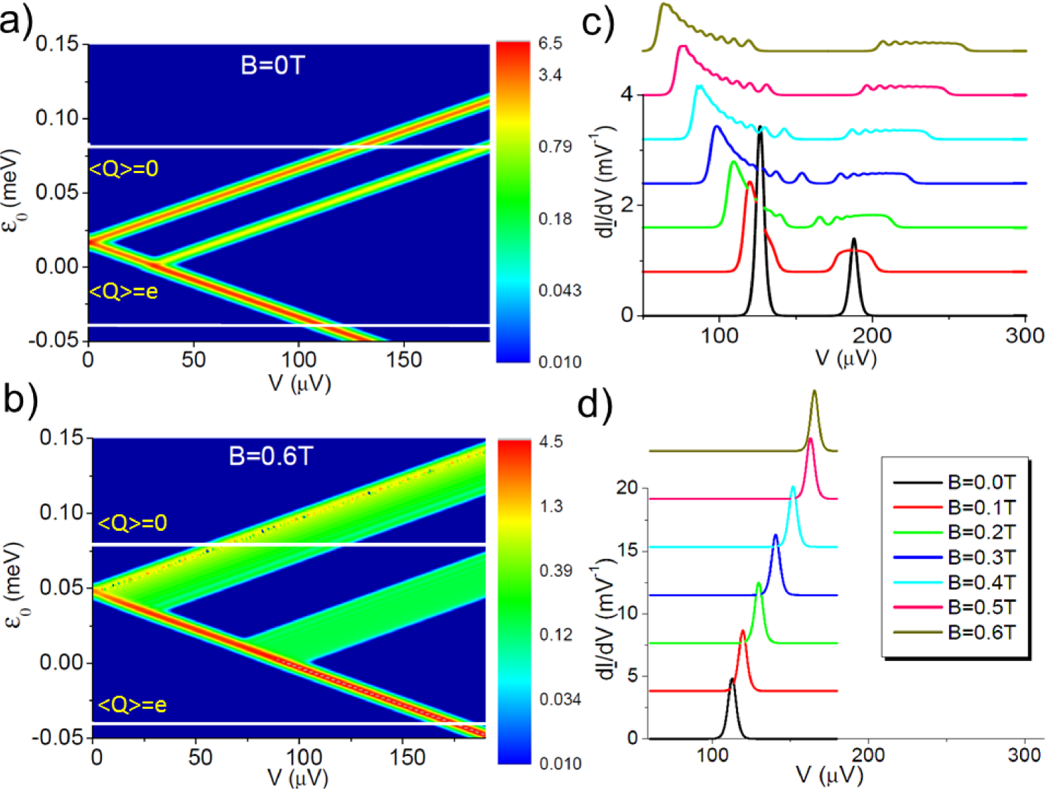
Let us consider first the case (left panel in Fig. 3). At mK only the ground state(s) is (are) occupied. Thus, a single transition is seen, from the to the states. As the magnetic field is ramped, the energy of the transition increases, reflecting the electronic Zeeman shift. In contrast, in the case (right panel in Fig. 3), all the Zeeman split nuclear levels are equally populated, even down to mK temperatures. Spin conservation selection rule implicit in Eq. (2) connects these 10 quasi-degenerate states of the manifold to the hyperfine spin-split levels of the manifold with different energies. As a result, the curve reveals 2 peaks at zero field, reflecting the splitting between the and states. At higher fields, the two zero-field peaks split in up to 10 peaks, that can be resolved at low enough temperature [see Figs. 3c) and 4b)].
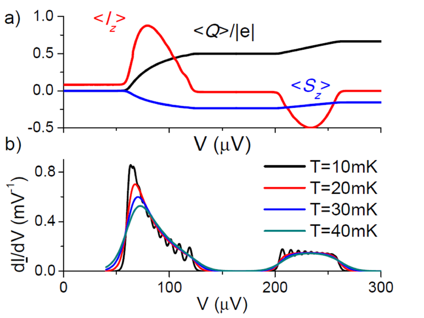
Interestingly, the application of a bias to the state, for which the nuclear spin states are randomized, can result in a finite average nuclear magnetic moment. We show this in Fig. 4a) for finite . At zero bias, the charge of the dopant level is , and the nuclear spins are randomized. When the bias hits the addition energy a selective depopulation of a given level of the manifold starts, in favor of a state that mixes the and components, resulting in a net accumulation of nuclear spin. When all the transitions to the manifold are allowed, the nuclear spin vanishes again. Then, when the bias permits the transitions to the manifold, the nuclear spin accumulation starts in the opposite direction. Thus, when matches the center of the multiplet, see Fig. 4a), the nuclear spins tend to align antiparallel to the electronic spin. Then, when reaches the center of the multiplet, the nuclear spins prefer aligning parallel to the electronic spin.
Whereas all our results discussed so far refer to steady state conditions, it is worth pointing out that there are two very different time scales in the dynamics of the system. Whereas the charge equilibrates in the dopant level in a time scale set by , the nuclear spin relaxation, dominated by many events of hyperfine exchange with the electronic spin and subsequent recharging of the Bi, Besombes et al. (2008) takes place at a much longer time scale, hundreds of time larger than , but still much shorter than the intrinsic time of the nuclear spin. Thus, charge fluctuations in the Bi induce nuclear spin relaxation.Besombes et al. (2008)
We finally discuss the experimental feasibility of our proposal with state of the art techniques. First, according to our simulations, see Fig. 4b), the finite field hyperfine splitting is resolved at 10 mK but not a 20 mK. At 40 mK the 2 humps associated to the and manifolds are clearly resolved. Keeping the transport in the sequential tunneling regime requires that , which at 10mK, translates into pA. This is within reach of experimental setups.Kobayashi et al. (2011); Petta et al. (2008); Baugh et al. (2007); Morello et al. (2010); Jespersen et al. (2011)
In conclusion, we have studied the single electron transport spectroscopy of the hyperfine structure of a Bi dopant in a silicon nanotransistor. We have shown that, at sufficiently low temperatures, and when the dopant is ionized with a gate, the corresponding to sequential transport can resolve the hyperfine spectrum of the electron in the donor level. In addition, the non-equilibrium transport at finite field results in a hyper polarization of the nuclear spin state, or nuclear spin accumulation. These results are different from our previous work, where we considered the same system in a different transport regime, cotunneling, and we showed that inelastic cotunneling of the dopant in the state could also resolve the hyperfine spectrum and drive the nuclear spin states out of equilibrium.Delgado and Fernández-Rossier (2011) Future work should determine how, in the cotunneling regime, the appearance of the Kondo effect Tettamanzi et al. (2012) competes with the reported effect.
This work has been financially supported by MEC-Spain (Grant Nos. FIS2010-21883-C02-01, FIS2009-08744, and CONSOLIDER CSD2007-0010) as well as Generalitat Valenciana, grant Prometeo 2012-11.
References
- Sellier et al. (2006) H. Sellier, G. P. Lansbergen, J. Caro, S. Rogge, N. Collaert, I. Ferain, M. Jurczak, and S. Biesemans, Phys. Rev. Lett. 97, 206805 (2006).
- Pierre et al. (2009) M. Pierre, R. Wacquez, X. Jehl, M. Sanquer, M. Vinet, and O. Cueto, Nature nanotechnology 5, 133 (2009).
- Lansbergen et al. (2010) G. P. Lansbergen, G. C. Tettamanzi, J. Verduijn, N. Collaert, S. Biesemans, M. Blaauboer, and S. Rogge, Nano Letters 10, 455 (2010).
- Tan et al. (2010) K. Y. Tan, K. W. Chan, M. Mottonen, A. Morello, C. Yang, J. v. Donkelaar, A. Alves, J.-M. Pirkkalainen, D. N. Jamieson, R. G. Clark, et al., Nano Letters 10, 11 (2010).
- Golovach et al. (2011) V. N. Golovach, X. Jehl, M. Houzet, M. Pierre, B. Roche, M. Sanquer, and L. I. Glazman, Phys. Rev. B 83, 075401 (2011).
- Fuechsle et al. (2012) M. Fuechsle, J. A. Miwa, S. Mahapatra, H. Ryu, S. Lee, O. Warschkow, L. C. L. Hollenberg, G. Klimeck, and M. Y. Simmons, Nature Nanotechnology 7, 242 (2012).
- Tettamanzi et al. (2012) G. C. Tettamanzi, J. Verduijn, G. P. Lansbergen, M. Blaauboer, M. J. Calderón, R. Aguado, and S. Rogge, Phys. Rev. Lett. 108, 046803 (2012).
- Kane (1998) B. Kane, Nature 393, 133 (1998).
- DiVincenzo et al. (2000) D. P. DiVincenzo, D. Bacon, J. Kempe, G. Burkard, and K. B. Whaley, Nature 408, 339 (2000).
- Ladd et al. (2010) T. D. Ladd, F. Jelezko, R. Laflamme, Y. N. Y, C. Monroe, and J. L. O’Brien, Nature 464, 45 (2010).
- Elzerman et al. (2004) J. M. Elzerman, R. Hanson, L. H. W. van Beveren, B. Witkamp, L. M. K. Vandersypen, and L. P. Kouwenhoven, Nature 430, 431 (2004).
- Morello et al. (2010) A. Morello, J. J. Pla, F. A. Zwanenburg, K. W. Chan, K. Y. Tan, H. Huebl, M. Möttönen, C. D. Nugroho, C. Yang, J. A. v. Donkelaar, et al., Nature 467, 687 (2010).
- Neumann et al. (2010) P. Neumann, J. Beck, M. Steiner, F. Rempp, H. Fedder, P. R. Hemmer, J. Wrachtrup, and F. Jelezko, Science 329, 542 (2010).
- Fu et al. (2004) K.-M. C. Fu, T. D. Ladd, C. Santori, and Y. Yamamoto, Phys. Rev. B 69, 125306 (2004).
- Sleiter et al. (2010) D. Sleiter, N. Y. Kim, K. Nozawa, T. D. Ladd, M. L. W. Thewalt, and Y. Yamamoto, New Journal of Physics 12, 093028 (2010).
- Petta et al. (2008) J. R. Petta, J. M. Taylor, A. C. Johnson, A. Yacoby, M. D. Lukin, C. M. Marcus, M. P. Hanson, and A. C. Gossard, Phys. Rev. Lett. 100, 067601 (2008).
- Reilly et al. (2008) D. J. Reilly, J. M. Taylor, J. R. Petta, C. M. Marcus, M. P. Hanson, and A. C. Gossard, Science 321, 817 (2008).
- Foletti et al. (2009) S. Foletti, H. Bluhm, D. Mahalu, V. Umansky, and A. Yacoby, Nature Physics 5, 903 (2009).
- Kobayashi et al. (2011) T. Kobayashi, K. Hitachi, S. Sasaki, and K. Muraki, Phys. Rev. Lett. 107, 216802 (2011).
- George et al. (2010) R. E. George, W. Witzel, H. Riemann, N. V. Abrosimov, N. Nötzel, M. L. W. Thewalt, and J. J. L. Morton, Phys. Rev. Lett. 105, 067601 (2010).
- Morley et al. (2010) G. W. Morley, M. Warner, A. M. Stoneham, P. T. Greenland, J. van Tol, C. W. M. Kay, and G. Aeppli, Nature Materials 9, 725 (2010).
- Mohammady et al. (2010) M. H. Mohammady, G. W. Morley, and T. S. Monteiro, Phys. Rev. Lett. 105, 067602 (2010).
- Sekiguchi et al. (2010) T. Sekiguchi, M. Steger, K. Saeedi, M. L. W. Thewalt, H. Riemann, N. V. Abrosimov, and N. Nötzel, Phys. Rev. Lett. 104, 137402 (2010).
- Delgado and Fernández-Rossier (2011) F. Delgado and J. Fernández-Rossier, Phys. Rev. Lett. 107, 076804 (2011).
- Efros et al. (2001) A. L. Efros, E. I. Rashba, and M. Rosen, Phys. Rev. Lett. 87, 206601 (2001).
- Fernández-Rossier and Aguado (2007) J. Fernández-Rossier and R. Aguado, Phys. Rev. Lett. 98, 106805 (2007).
- Cohen-Tannoudji et al. (1998) C. Cohen-Tannoudji, G. Grynberg, and J. Dupont-Roc, Atom-Photon Interactions (Wiley and Sons, INC., New York, 1998).
- Besombes et al. (2008) L. Besombes, Y. Leger, J. Bernos, H. Boukari, H. Mariette, J. P. Poizat, T. Clement, J. Fernández-Rossier, and R. Aguado, Phys. Rev. B 78, 125324 (2008).
- Baugh et al. (2007) J. Baugh, Y. Kitamura, K. Ono, and S. Tarucha, Phys. Rev. Lett. 99, 096804 (2007).
- Jespersen et al. (2011) T. S. Jespersen, K. Grove-Rasmussen, J. Paaske, K. Muraki, T. F. an J. Nygård, and K. Flensberg, Nature Physics 7, 348 (2011).