Propagation effects in high-harmonic generation from dielectric thin films
Abstract
Theoretical investigation is conducted of high-order harmonic generation (HHG) in silicon thin films to elucidate the effect of light propagation in reflected and transmitted waves. The first-principles simulations are performed of the process in which an intense pulsed light irradiates silicon thin films up to 3 m thickness. Our simulations are carried within the time-dependent density functional theory (TDDFT) with the account of coupled dynamics of the electromagnetic fields and the electronic motion. It was found that the intensity of transmission HHG gradually decreases with the thickness, while the reflection HHG becomes constant from a certain thickness. Detailed analyses show that transmission HHG have two origins: the HHG generated near the front edge and propagating to the back surface, and that generated near the back edge and emitted directly. The dominating mechanism of the transmission HHG is found to depend on the thickness of the thin film and the frequency of the HHG. At the film thickness of 1 m, the transmission HHG with the frequency below 20 eV is generated near the back edge, while that with the frequency above 20 eV is generated near the front edge and propagates from there to the back surface.
I Introduction
The phenomenon of high-order harmonic generation (HHG) from solids irradiated with an intense ultrashort pulsed light has been very actively studied in recent years Ghimire et al. (2011); Schubert et al. (2014); Vampa et al. (2015a); Hohenleutner et al. (2015); Luu et al. (2015); Langer et al. (2017); You et al. (2017); Liu et al. (2017); Shirai et al. (2018); Vampa et al. (2018a); Orenstein et al. (2019); Ghimire and Reis (2019); Li et al. (2020); Goulielmakis and Brabec (2022). Apart from being at the focus of basic science, there is a strong interest from the perspective of applications, such as the creation of compact XUV light sources. Numerous experimental investigations have been conducted on HHG in various targets including simple dielectrics, two-dimensional materials Yoshikawa et al. (2017); Liu et al. (2017); Xia et al. (2018); Le Breton et al. (2018); Yoshikawa et al. (2019), topological materials Bai et al. (2021); Heide et al. (2022), and so on. Light pulses of linear, circular, or elliptical polarization have been used. Frequencies of light pulses range from terahertz to visible light. It has been shown that the HHG spectrum depends sensitively on the angle between the polarization direction of the light pulse and the crystal axes Langer et al. (2017); You et al. (2017); Neufeld et al. (2019).
There have also been conducted numerous theoretical studies of HHG from solids examining the motion of electrons in a single unit cell of a crystal Yue and Gaarde (2022). Extensive discussions have been conducted on the mechanisms of HHG, either interband electronic transitions or intraband electronic motion. Various theoretical approaches have been tried such as a one-dimensional modelHansen et al. (2017, 2018); Jin et al. (2019); Ikemachi et al. (2017), the time-dependent Schrödinger equation Wu et al. (2015); Apostolova and Obreshkov (2018), density matrix models Ghimire et al. (2012); Vampa et al. (2014, 2015b), the Floquet theory Faisal and Kamiński (1997); Faisal et al. (2005), and ab initio descriptions such as the time-dependent density functional theory (TDDFT) Otobe (2012, 2016); Tancogne-Dejean et al. (2017); Floss et al. (2019); Tancogne-Dejean et al. (2022); Freeman et al. (2022).
To explore HHG from solids, light propagation effects are another important issue to be considered Orenstein et al. (2019); Hussain et al. (2021). In the case of HHG from thin films, there appear higher-order harmonics in both transmitted and reflected waves Vampa et al. (2018b); Xia et al. (2018), which we call reflection HHG (RHHG) and transmission HHG (THHG), respectively, for which propagation effects work differently. There has also been interest in HHG from three-dimensional nanostructures to produce intense and characteristic HHG Vampa et al. (2017); Liu et al. (2018). The precise way in which HHG depends on the shape of the nanostructure can only be investigated by examining the propagation effects.
Theoretical studies of HHG considering light propagation effects have come to be actively studied recently Lorin et al. (2007); Ghimire et al. (2012); Floss et al. (2018); Orlando et al. (2019); Kilen et al. (2020); Yamada and Yabana (2021); Wu et al. (2022); Jensen and Madsen (2022). For such studies, it is necessary to couple the description of electronic motion with the Maxwell equations which describe the light propagation.
We previously reported the light propagation effect on RHHG and THHG from silicon films of thickness up to 200 nm Yamada and Yabana (2021). In that work, we developed and utilized the first-principles approaches combining the TDDFT for electronic motion with the Maxwell equations in two different schemes. For relatively thin (thick) films, calculations were performed using the single-scaleYamada et al. (2018) (multiscaleYabana et al. (2012)) Maxwell-TDDFT method in which the Maxwell and TDKS equations are coupled without (with) a coarse-graining approximation. It was found that the HHG signals are strongest in both the reflection and transmission waves at the film thickness of 2–15 nm. It was also found that there appears a clear interference effect in the RHHG.
In the present work, we extend the first-principles Maxwell-TDDFT approach of the previous study to much thicker films up to 3 m using the multiscale method with the course-graining approximation. We suggest that it is important to clarify the propagation effect for materials whose size is comparable or larger than the wavelength of the laser pulse. Indeed, as will be shown, we find two kinds of propagation effects for films of about 1 m thickness. One is the nonlinear propagation effect of the intense incident pulse in the frequency region of the fundamental wave. Another is the propagation of the generated high harmonic wave that is described by the linear optical response in a wide spectral region.
II Theoretical methods
II.1 Single unit-cell calculation
We first consider a simulation of the electronic motion in a unit cell of a crystalline solid driven by a pulsed electric field with a given time profile. In the real time TDDFT, the electronic motion is described by the following time-dependent Kohn-Sham (TDKS) equation for the time-dependent Bloch orbitals Bertsch et al. (2000); Otobe et al. (2008),
| (1) |
with the Hamiltonian
| (2) | |||||
Here we treat dynamics of the valence electrons with the norm-conserving pseudopotential Troullier and Martins (1991). The scalar potential, , is periodic and satisfies the equation
| (3) |
where ionic charge density is prepared so that to produce the local part of the pseudopotential in . The density of electrons, , is given by
| (4) |
where is the number of -points. The sum is taken over the occupied bands in the ground state. The nonlocal part of the pseudopotential is modified as , where is the usual separable form of the norm-conserving pseudopotential Kleinman and Bylander (1982). is the exchange-correlation potential for which the adiabatic local-density approximation Perdew and Zunger (1981) is assumed.
The Bloch orbitals are initially set to the ground state solution. Solving the TDKS equation, we obtain the electric current density averaged over the unit-cell volume as
| (5) |
Taking the Fourier transformation of the current, we obtain a spectrum that will be used to analyze HHG,
| (6) |
Here we introduce a smoothing function . is the total calculation time.
II.2 Multiscale Maxwell-TDDFT calculation
We consider an irradiation of a free-standing thin film of thickness in a vacuum by an ultrashort light pulse of a linearly polarized plane wave at the normal incidence. The multiscale Maxwell-TDDFT methodYabana et al. (2012) is used to describe the light propagation. In the method, we combine the one-dimensional Maxwell equation that describes the light propagation and a number of TDKS equations that describe the electonic motion using a course-graining approximation.
The light propagation is described in the macroscopic scale by solving the following wave equation:
| (7) |
where is the macroscopic coordinate. and are the vector potential and the current density, respectively. This wave equation is solved using a one-dimensional grid for the variable. At each grid point of inside the film, we consider an infinite crystalline system of the film material. The electronic motion at each grid point is described by the Bloch orbitals which satisfy the TDKS equation:
| (8) |
where the Kohn-Sham Hamiltonian is given by Eq. (2). Here, the scalar potential and the exchange-correlation potential depend on . The macroscopic current density at each is expressed using Eq. (5) as
| (9) |
By solvingy Eqs. (7), (8) and (9) simultaneously, we obtain the solution for a given initial pulse that is prepared in the vacuum region in front of the thin film. At the beginning of the calculation, the Bloch orbitals are set to those of the ground state for all grid points of .
The multiscale Maxwell-TDDFT calculation provides the time profile of the electric field, . The time profiles of the reflected and transmitted fields are given by those at the grid points of the front () and back () edges, respectively, where the incident pulse is subtracted for the former. We evaluate the HHG spectra via the square of the Fourier-transformed electric field , where is defined by
| (10) |
Here, is the total calculation time for which we use fs. In Eq. (10), we use again a smoothing function to remove noises that originate from the end of the pulse. We further apply a frequency averaging using the Gaussian convolution as follows:
| (11) |
Here we will use a.u. When we examine strength of the th-order harmonics, we will use:
| (12) |
where is the frequency of the fundamental wave.
II.3 Numerical detail
We utilize an open-source software package SALMON (Scalable Ab initio Light-Matter simulator for Optics and Nanoscience)Noda et al. (2019); SAL for which some of the present authors are among the leading developers. In this code, solutions for the electronic orbitals as well as the electromagnetic fields are found by using the finite-difference method. The time evolution of the electron orbitals is carried out using the Taylor expansion method Yabana and Bertsch (1996).
In solving the TDKS equation, we use a conventional unit cell of the diamond structure containing eight Si atoms with the lattice constant of nm. The numbers of grid points for discretizing the unit cell volume and the Brillouin zone are set to and , respectively. A uniform 1D grid is introduced to describe the wave equation of Eq. (7) with the grid spacing of nm, except the nm case where the grid spacing of nm is used, that is, the film is expressed as a single grid point. The time step is set to fs. We have carefully examined the convergence of the calculations with respect to the discretizations in spatial, -space, and time variables.
III Results and discussion
III.1 Single unit-cell calculation

Before discussing propagation effects in HHG, we show calculations of electronic motion and HHG spectrum in a unit cell of crystalline Si under a pulsed electric field of a given time profile. They will be useful to understand results of multiscale Maxwell-TDDFT calculations that involve complex coupling with light propagation.
We employ a pulsed electric field of linear polarization given by the following time profile for the vector potential,
| (13) |
Here is the maximum amplitude of the electric field, is the fundamental frequency, and is the total duration of the pulse. The value of the maximum amplitude will be specified later. In the following calculations, we set as 1.55 eV and 100 fs. The electric field is related to the vector potential by .
In Fig. 1, we show results of a typical calculation solving the TKDS equation (1). Panel (a) shows the applied pulse shape of Eq. (13) with the maximum amplitude of V/Å. Panel (b) shows the induced current density averaged over the unit cell volume given by Eq. (5). At the beginning of the calculation, the induced current looks proportional to the applied electric field. In fact, there is a phase shift of since the average frequency of the pulse is below the direct bandgap of Si that is equal to 2.6 eV in the local density approximation. At around the peak of the applied electric field and immediately after, there appear high-frequency oscillations in the current that are related to HHG. Panel (c) shows the electronic excitation energy per atom. Although the average frequency is below the bandgap energy, we find an increase of electronic excitation energy due to nonlinear excitation. The amount of the excitation energy after the applied electric field termination is about 0.68 eV per atom. We consider that this amount of the excitation energy is close to, but still below, the value that causes permanent damage to a surface of bulk SiBonse et al. (2002); Medvedev et al. (2015); Venkat and Otobe (2022a, b).
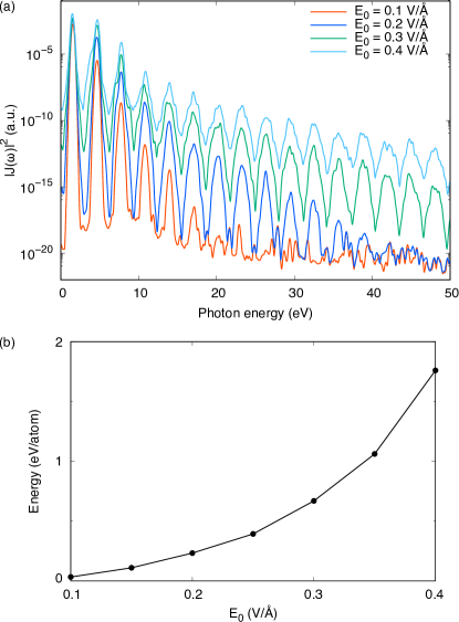
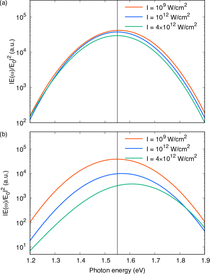
Figure 2(a) shows HHG spectra of single-cell calculations, Eq. (6), for applied pulses of several intensities, , , , and V/Å. The average frequency and the pulse duration are chosen to be common as = 1.55 eV and fs, respectively. As is evident from the figure, the HHG becomes more pronounced and extended to higher orders as the field amplitude increases. Clear HHG signals are seen up to 11th order for V/Å, up to 25th for V/Å, and more than 30th for V/Å. We note that production of HHG of very high order can be observed by using sufficiently long pulse, as we have shown previously Freeman et al. (2022).
Figure 2(b) shows the energy deposition to electrons after the pulse end. Since two photons are required to excite electrons across the direct bandgap, the energy deposition should scale as at low intensity region. For the pulse of the maximum amplitude of 0.35 eV/Å, the energy deposition per atom exceeds 1.0 eV per atom that eventually leads, as we mentioned previously, to a permanent damage to the material. These results indicate that a pulse of maximum amplitude around 0.3 V/Å produces HHG of very high orders extending beyond 50 eV, while avoiding to produce permanent damage to the material.
III.2 Multiscale calculation
III.2.1 Light propagation
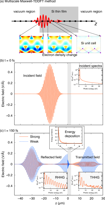
Figure 3 summarizes an overview of the multiscale Maxwell-TDDFT calculation for the light propagation of a pulsed light through a Si thin film. Figure 3(a) shows a schematic view of the numerical method. The light propagation is solved on a uniform 1D grid along the -axis. At each grid point inside the thin film, electron dynamics calculation is carried out in a unit cell of Si. In the figure, electron density changes driven by the light pulse are illustrated for the first three grid points of the -coordinate.
Figure 3(b) and (c) show snapshots of the electric field of the light pulse propagating through a Si thin film of nm thickness. In Fig. 3(b), the electric field of the initial pulse ( fs) that locates in front of the film is shown where the film is exhibited as a thin gray area. The initial pulse with the time profile given by Eq. (13) is used with the fundamental frequency of eV, total duration of fs, and the maximum intensity of W/cm2 that corresponds to V/Å. Note that the maximum field amplitude and the maximum intensity is related by . In Fig. 3(c), a snapshot of the electric field at fs is shown. Here we display results corresponding to initial pulses of two different maximum intensities, W/cm2 by red-solid line and W/cm2 by blue-dotted line, respectively. For the weaker pulse of the initial intensity of W/cm2, linear propagation is expected. In the figure, the field is multiplied by a factor of so that the differences of two lines manifest nonlinear effects in the stronger pulse. In the snapshot, reflected and transmitted pulses are seen. They are apart from the film (left for the reflected and right for the transmitted pulses). There also appears a component around the film that is caused by a reflection at the back surface of the film.
It can be observed that the nonlinear effects appear more significantly in the transmitted pulse than in the reflected pulse. While the envelopes of the reflected pulses of the weaker and the stronger cases look similar to each other and do not change much from the envelope of the initial pulse, the transmitted pulse of the stronger case suffers a strong nonlinear effect with the nearly flat envelope. This can be understood as follows: During the propagation, the high field component of the electric field excites efficiently electrons in the medium and, as the reaction, the amplitude of the high field part is reduced to produce the flat envelope in the transmitted pulse.
As the inset of Fig. 3(c), the energy deposition from the light field to electrons in the unit cell is shown as a function of . At the front surface, the energy deposition is about 0.5 eV/atom and is close to the case of 0.25 V/Å pulse in the single unit-cell calculation shown in Fig. 2(b). Since the electric field at the front surface is given as the sum of those of the incident and the reflected pulses, the maximum electric field at the front surface is smaller than that of the incident pulse that is more than 0.5 V/Å. As we noted previously, this amount of the energy deposition will not cause a permanent damage to the material. The fluence of the incident pulse is about 0.09 J/cm2 and this value is substantially smaller than 0.2 J/cm2, which is the reported threshold value of Si modificationBonse et al. (2002). The energy deposition at the front surface, 0.5 eV/atom, is also smaller than 0.65 eV/atom, which is the theoretical value of the threshold for the phase transitionMedvedev et al. (2015). The energy deposition shows the maximum value at the front surface and decays quickly inside the material, less than 0.1 eV/atom at 200 nm from the surface. This is because the high amplitude component of the light pulse is reduced during the propagation by nonlinear interaction.
III.2.2 HHG spectra
A Fourier spectrum [Eq. (10)] of the incident pulse is shown in the inset of Fig. 3(b), and those of the reflected and transmitted pulses (RHHG and THHG) are shown in the insets of Fig. 3(c) for the case of a strong incident pulse of W/cm2. We note that all the Fourier transforms are taken with a sufficiently long duration of fs, in which the pulse reflected at the back surface is included in the RHHG. It can be seen that, although both the reflected and transmitted pulses include HHG components, RHHG shows clear signals of higher orders than THHG.
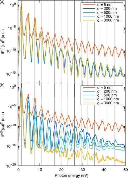
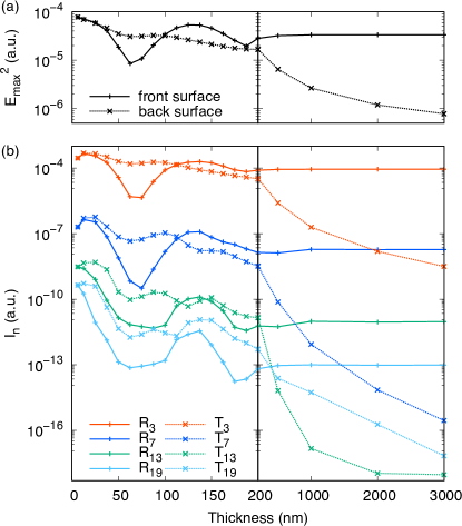
We next examine thickness dependence of RHHG and THHG. Figure 4(a) and (b) show spectra of RHHG and THHG, respectively, for Si films with thickness of 5, 200, 500, 1000, and 3000 nm. The incident pulse is chosen to be the same as that shown in Fig. 3(b). Figure 5 shows thickness dependence of RHHG and THHG at several harmonics orders for films of various thickness up to 3000 nm. In Fig. 5(b), strengths of RHHG (solid lines) and THHG (dotted lines) given by Eq. (12) are shown for the 3rd (4.65 eV), 7th (10.85 eV), 13th (20.15 eV), and 19th (29.45 eV) harmonics. In Fig. 5(a), a square of the maximum amplitude of the electric field in time, , are shown at the front surface (solid line) and back surface (dotted line) of the film. We note that a similar plot was provided in Fig. 5 of Ref Yamada and Yabana, 2021 up to 200 nm thickness.
As is seen from Fig. 4(a) and (b) and Fig. 5(b), spectra of RHHG and THHG for the film thickness of 5 nm are almost identical with each other and are the strongest among signals of films of different thicknesses. These features have already been reported in our previous analysis Yamada and Yabana (2021) and can be understood in terms of two-dimensional approximation for electromagnetism that is valid for very thin films.
In Fig. 5(b), there appears an oscillatory behavior as a function of thickness, clearly in RHHG and vaguely in THHG, below 200 nm. It originates from the interference effect that is seen in Fig. 5(a) at the front surface Yamada and Yabana (2021). Since the average frequency of the incident pulse, eV is below the direct bandgap of Si that is 2.6 eV in the present LDA calculation, the propagation is regarded as in a transparent medium in linear optics. Then, we expect that the electric field at the front surface suffers a cancellation if the thickness is equal to , where is the wavelength of incident light, is the index of refraction, and is an integer. In Fig. 5(a), the maximum amplitude shows a dip at the thickness of nm. This corresponds to case using the value of index of refraction, . However, such an interference effect soon becomes ineffective as the thickness increases since the strong pulse attenuates quickly during the propagation due to nonlinear excitation processes. As seen in Fig. 5(a), the next cancellation expected at around nm is less clear. We should note that the thickness at which the interference disappears depends strongly on the choice of the intensity of the initial pulse. In the present setting, we consider that the interference is no more important for films thicker than 200 nm.
In both Figs. 4(b) and 5(b), as the thickness increases from 200 nm to 3000 nm, the RHHG signals change little by the thickness. Meanwhile, the THHG signals decrease substantially and monotonically with the thickness increase. These trends look to follow the thickness dependence of the maximum amplitude of the electric field at the front and the back surfaces shown in Fig. 4(a). This finding indicates that RHHG (THHG) is dominantly produced at the front (back) surfaces. However, there takes place more complex dynamics that can be found if we look carefully the thickness dependence of THHG.
We focus on the THHG generated from the film of thickness nm that is shown by light blue line in Figs. 4(b). At this thickness, we find an appearance of a dip in THHG at around 20 eV. Looking at the spectrum carefully, peaks of THHG below 20 eV show blue shift, while peaks above 20 eV do not. We also note that THHG spectrum for the film of nm thickness has no longer clear peaks except for a few peaks at low frequency region. To understand the mechanism that causes these features, we make an analysis decomposing propagating pulse into frequency window in the next subsection.
III.2.3 Analysis using frequency windows
To understand mechanisms that produce characteristic features of THHG mentioned above, we investigate the pulse propagation behavior separating frequency regions using a filtered inverse-Fourier transformation as described below. Once the multiscale Maxwell-TDDFT calculation is finished, we take a Fourier transformation to obtain the electric field in the frequency domain at each grid point , . We then perform the inverse-Fourier transformation with the frequency window as follows,
| (14) |
As the window function for filtering the frequency region, , we use the Blackman window function,
| (15) |
where is the central frequency and the frequency width is set as eV.
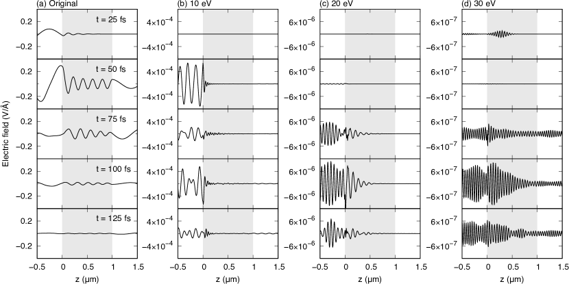
Figure 6(a) shows snapshots of the electric field at , , , , and fs for a pulse propagation through the Si thin film of nm thickness. The gray area indicates the Si thin film. We note that the incident pulse ends at fs. Figure 6(b), (c), and (d) show frequency-gated snapshots of the propagating pulse using the filtered inverse-Fourier transform of Eq. (14) with the central frequency of , 20, and 30 eV, respectively.
We first look at Fig. 6(a) which shows snapshots of the whole pulse. The amplitude is maximal at fs at the front surface. Since HHG depends strongly on the amplitude of the electric field as shown in Fig. 2(a), HHG takes place most efficiently at this moment and at around the front surface.
We next look at eV case shown in Fig. 6(b). There appears a strong reflection wave that corresponds to the RHHG around 10 eV which is produced at the front surface. However, inside the medium, the wave generated at the front surface attenuates quickly as it propagates. This is because silicon is strongly absorptive at around 10 eV in linear optics. Nevertheless, we find a weak transmitted wave at and 125 fs that should correspond to the THHG around 10 eV. This THHG should be produced at the back surface of the film. As seen in Fig. 6(a) at fs, there is an electric field of amplitude about 0.1 V/Å at around the back surface that can produce HHG up to 20 eV, as shown in Fig. 2.
The waveform looks similar at 20 eV region, as shown in Fig. 6(c), except for one important difference. There appears no visible transmission wave at and 125 fs. This can be understood by noting that the electric field at the back surface, shown in Fig. 6(a) at fs, is not large enough to produce HHG around 20 eV.
In contrast, at 30 eV case shown in Fig. 6(d), the HHG wave produced at the front surface does not attenuate completely and appears as the transmitted wave. It indicates that THHG at 30 eV region is mainly produced at the front surface and propagate through the film.
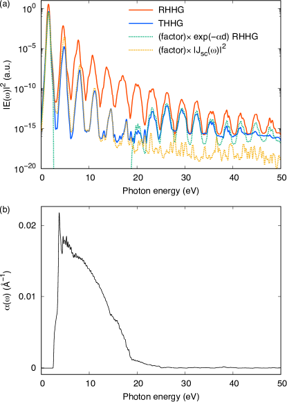
To verify the different mechanisms of THHG below and above 20 eV described above, we revisit RHHG and THHG spectra emitted from the 1000 nm Si thin film that is shown again in Fig. 7(a) by red and blue solid lines, respectively. As we found in Fig. 6(d), the THHG around 30 eV is produced at the front surface and propagates through the film. Then we may expect that such THHG spectrum is proportional to the RHHG spectrum multiplied by the penetration factor where is the attenuation coefficient calculated from the dielectric function of Si. This is plotted by green dotted line in Fig. 7(a) for which a constant factor is multiplied to roughly coincide with the THHG spectrum around 30 eV. The attenuation coefficient used in the plot is shown in Figure 7(b) that is calculated by linear response TDDFT. Above 20 eV, the dielectric function of Si becomes rather transparent and the penetration factor is close to unity. In the frequency region from 3 to 20 eV, the green dotted line in Fig. 7(a) becomes extremely small due to the penetration factor and cannot explain the THHG spectrum. From these observations, we can support the hypothesis that THHG above 20 eV is indeed generated from the front surface.
To confirm that THHG below 20 eV is generated at the back surface, we carry out the following analysis. We first examine the electric field at the front and the back surfaces in frequency domain around the fundamental frequency. In Fig. 8(a), spectra of electric fields at the front surface are compared for three different intensities of the incident pulse, W/cm2 (red line), W/cm2 (blue line), and W/cm2 (green line). They are shown with a normalization such that the incident pulse has the same amplitude. In Fig. 8(b), the same spectra but at the back surface are shown. We observe the following facts. For the electric field at the front surface, the peak is equal to the average frequency of the incident pulse, eV, irrespective of the intensity. For the electric field at the back surface, the peak position does not change for the weak intensity case of W/cm2. However, as the intensity increases, the peak is blue-shifted. At the intensity W/cm2, the peak position becomes eV. We thus find that there is a nonlinear effect that blue-shifts the peak frequency during the propagation. As we noted previously in Fig. 4(b), THHG below 20 eV shows blue-shift in the frequency as the intensity increases. This blue-shift can be naturally understood if we consider that the THHG below 20 eV is generated at the back surface.
To further assure this mechanism, we carry out the following analysis: We first extract the fundamental wave component from the electric field at the back surface, removing the HHG component. For this purpose, we make the inverse-Fourier transformation of Eq. (14) using the following window function,
| (16) |
with eV, and eV. Using the electric field thus obtained, we perform a single unit cell calculation described in Sec. IIA. We show the calculated spectrum multiplied by a constant as the orange dotted line in Fig. 7(a). As seen in the figure, THHG (blue line) and the orange dotted line agree well with each other, not only in relative intensity of each order but also in positions of the peak frequency. Since the electric field at the back surface is rather weak, it cannot produce harmonics above 20 eV. From these analyses, we conclude that THHGs below and above 20 eV have different origins and the dip at 20 eV appears due to the combination of two mechanisms.
After gaining a detailed understanding of the mechanism of THHG, we revisit thickness dependence of THHG shown in Fig. 5(b). As we mentioned previously, THHG signals decrease as the thickness increases from 200 nm to 3000 nm. A closer look at the figure shows that the decreasing behavior of the signal depends on the order. While the THHG signal of 19th order decreases exponentially (linearly in logarithmic plot), signals of other orders behave differently. Such difference of the signals can be understood by the different mechanisms of THHG discussed previously. Since THHG below 20 eV is generated at the back surface, the intensities of the 3rd and 7th harmonics are expected to behave as the 3rd and 7th power of the intensity of the fundamental wave at the back surface. On the other hand, the 19th HHG signal, whose frequency is about 30eV, is generated at the front surface and its thickness dependence is expected to be determined by the penetration factor, . These explanations are consistent with the results shown in Fig. 5(b). For the 13th harmonic that corresponds to about the dip position of the spectrum at 20 eV, the THHG signal exhibits complex dependencies reflecting the competition between the two mechanisms.
IV Summary
We have investigated the impact of propagation effects on high-order harmonic generation (HHG) in reflection and transmission pulses (RHHG and THHG) from silicon (Si) thin films. Using the multiscale Maxwell-TDDFT method, we calculated the spectrum of RHHG and THHG for Si films of various thickness up to 3000 nm and explored physical mechanisms that determines their behavior. The fundamental frequency of the incident pulse is set to 1.55 eV, well below the direct bandgap of Si. We have found the three following mechanisms to play an important role: (1) Propagation effect on the strong pulse in the frequency region of the incident pulse. (2) Generation of HHG that predominantly takes place at either the front or the back surfaces. (3) Propagation effect on the generated high harmonic waves under a linear light-matter interaction.
We first note that HHG takes place efficiently at the front surface since HHG is quite sensitive to the amplitude of the electric field and it attenuates quickly as it propagate inside the thin film. RHHG is considered to be produced at the front surface. We reported previously that the intensity of RHHG depends sensitively on the thickness of the film for thickness less than 200 nm, because of the linear interference effect inside the thin film. In the present work, we have found that the interference effect becomes less important for films above 200 nm, since the propagating wave inside the film attenuates quickly.
Propagation effects appear in more complex way in THHG. It shows different behavior in the frequency regions below and above 20 eV. This distinction comes from the linear absorption property of Si, strongly absorptive below and almost transparent above 20 eV. THHG signals appear in the transmitted wave after the propagation inside the thin film. Then THHG that produced at the front surface attenuates quickly for components below 20 eV. It was found that THHG in the frequency region below 20 eV is produced at the back surface. It is also observed that THHG below 20 eV shows blue-shift in the peak positions. This blue-shift can be understood in terms of the nonlinear propagation effect of the pulse in the fundamental frequency region.
The present results show that the propagation dynamics causes interesting and significant effects in HHG from Si films of nano- to micro-meter thickness and that the multiscale Maxwell-TDDFT scheme provides a reliable description for them. Since the method can be applicable for three-dimensional nano-materials Uemoto, Mitsuharu et al. (2019), it is expected to be useful to design and simulate optimal nano-materials that work as efficient HHG sources.
Acknowledgements.
This research was supported by JST-CREST under grant number JP-MJCR16N5, and by MEXT Quantum Leap Flagship Program (MEXT Q-LEAP) Grant Number JPMXS0118068681, and by JSPS KAKENHI Grant Number 20H2649. Calculations are carried out at Fugaku supercomputer under the support through the HPCI System Research Project (Project ID: hp220120), and Multidisciplinary Cooperative Research Program in CCS, University of Tsukuba.References
- Ghimire et al. (2011) S. Ghimire, A. D. DiChiara, E. Sistrunk, P. Agostini, L. F. DiMauro, and D. A. Reis, Nat. Phys. 7, 138 (2011).
- Schubert et al. (2014) O. Schubert, M. Hohenleutner, F. Langer, B. Urbanek, C. Lange, U. Huttner, D. Golde, T. Meier, M. Kira, S. W. Koch, et al., Nat. Photonics 8, 119 (2014).
- Vampa et al. (2015a) G. Vampa, T. J. Hammond, N. Thiré, B. E. Schmidt, F. Légaré, C. R. McDonald, T. Brabec, and P. B. Corkum, Nature 522, 462 (2015a).
- Hohenleutner et al. (2015) M. Hohenleutner, F. Langer, O. Schubert, M. Knorr, U. Huttner, S. W. Koch, M. Kira, and R. Huber, Nature 523, 572 (2015).
- Luu et al. (2015) T. T. Luu, M. Garg, S. Y. Kruchinin, A. Moulet, M. T. Hassan, and E. Goulielmakis, Nature 521, 498 (2015).
- Langer et al. (2017) F. Langer, M. Hohenleutner, U. Huttner, S. W. Koch, M. Kira, and R. Huber, Nat. Photonics 11, 227 (2017).
- You et al. (2017) Y. S. You, D. A. Reis, and S. Ghimire, Nat. Phys. 13, 345 (2017).
- Liu et al. (2017) H. Liu, Y. Li, Y. S. You, S. Ghimire, T. F. Heinz, and D. A. Reis, Nat. Phys. 13, 262 (2017).
- Shirai et al. (2018) H. Shirai, F. Kumaki, Y. Nomura, and T. Fuji, Opt. Lett. 43, 2094 (2018).
- Vampa et al. (2018a) G. Vampa, T. J. Hammond, M. Taucer, X. Ding, X. Ropagnol, T. Ozaki, S. Delprat, M. Chaker, N. Thiré, B. E. Schmidt, et al., Nat. Photonics 12, 465 (2018a).
- Orenstein et al. (2019) G. Orenstein, A. Julie Uzan, S. Gadasi, T. Arusi-Parpar, M. Krüger, R. Cireasa, B. D. Bruner, and N. Dudovich, Opt. Express 27, 37835 (2019).
- Ghimire and Reis (2019) S. Ghimire and D. A. Reis, Nat. Phys. 15, 10 (2019).
- Li et al. (2020) J. Li, J. Lu, A. Chew, S. Han, J. Li, Y. Wu, H. Wang, S. Ghimire, and Z. Chang, Nat. Commun. 11, 2748 (2020).
- Goulielmakis and Brabec (2022) E. Goulielmakis and T. Brabec, Nature Photonics 16, 411 (2022).
- Yoshikawa et al. (2017) N. Yoshikawa, T. Tamaya, and K. Tanaka, Science (80-. ). 356, 736 (2017).
- Xia et al. (2018) P. Xia, C. Kim, F. Lu, T. Kanai, H. Akiyama, J. Itatani, and N. Ishii, Opt. Express 26, 29393 (2018).
- Le Breton et al. (2018) G. Le Breton, A. Rubio, and N. Tancogne-Dejean, Phys. Rev. B 98, 165308 (2018).
- Yoshikawa et al. (2019) N. Yoshikawa, K. Nagai, K. Uchida, Y. Takaguchi, S. Sasaki, Y. Miyata, and K. Tanaka, Nat. Commun. 10, 3709 (2019).
- Bai et al. (2021) Y. Bai, F. Fei, S. Wang, N. Li, X. Li, F. Song, R. Li, Z. Xu, and P. Liu, Nature Physics 17, 311 (2021).
- Heide et al. (2022) C. Heide, Y. Kobayashi, D. R. Baykusheva, D. Jain, J. A. Sobota, M. Hashimoto, P. S. Kirchmann, S. Oh, T. F. Heinz, D. A. Reis, et al., Nature Photonics 16, 620 (2022).
- Neufeld et al. (2019) O. Neufeld, D. Podolsky, and O. Cohen, Nat. Commun. 10, 405 (2019).
- Yue and Gaarde (2022) L. Yue and M. B. Gaarde, J. Opt. Soc. Am. B 39, 535 (2022).
- Hansen et al. (2017) K. K. Hansen, T. Deffge, and D. Bauer, Phys. Rev. A 96, 053418 (2017).
- Hansen et al. (2018) K. K. Hansen, D. Bauer, and L. B. Madsen, Phys. Rev. A 97, 043424 (2018).
- Jin et al. (2019) J.-Z. Jin, H. Liang, X.-R. Xiao, M.-X. Wang, S.-G. Chen, X.-Y. Wu, Q. Gong, and L.-Y. Peng, Phys. Rev. A 100, 013412 (2019).
- Ikemachi et al. (2017) T. Ikemachi, Y. Shinohara, T. Sato, J. Yumoto, M. Kuwata-Gonokami, and K. L. Ishikawa, Phys. Rev. A 95, 043416 (2017).
- Wu et al. (2015) M. Wu, S. Ghimire, D. A. Reis, K. J. Schafer, and M. B. Gaarde, Phys. Rev. A 91, 043839 (2015).
- Apostolova and Obreshkov (2018) T. Apostolova and B. Obreshkov, Diam. Relat. Mater. 82, 165 (2018).
- Ghimire et al. (2012) S. Ghimire, A. D. DiChiara, E. Sistrunk, G. Ndabashimiye, U. B. Szafruga, A. Mohammad, P. Agostini, L. F. DiMauro, and D. A. Reis, Phys. Rev. A 85, 043836 (2012).
- Vampa et al. (2014) G. Vampa, C. R. McDonald, G. Orlando, D. D. Klug, P. B. Corkum, and T. Brabec, Phys. Rev. Lett. 113, 073901 (2014).
- Vampa et al. (2015b) G. Vampa, C. R. McDonald, G. Orlando, P. B. Corkum, and T. Brabec, Phys. Rev. B 91, 064302 (2015b).
- Faisal and Kamiński (1997) F. H. M. Faisal and J. Z. Kamiński, Phys. Rev. A 56, 748 (1997).
- Faisal et al. (2005) F. H. M. Faisal, J. Z. Kamiński, and E. Saczuk, Phys. Rev. A 72, 023412 (2005).
- Otobe (2012) T. Otobe, J. Appl. Phys. 111, 093112 (2012).
- Otobe (2016) T. Otobe, Phys. Rev. B 94, 235152 (2016).
- Tancogne-Dejean et al. (2017) N. Tancogne-Dejean, O. D. Mücke, F. X. Kärtner, and A. Rubio, Phys. Rev. Lett. 118, 087403 (2017), eprint 1609.09298.
- Floss et al. (2019) I. Floss, C. Lemell, K. Yabana, and J. Burgdörfer, Phys. Rev. B 99, 224301 (2019).
- Tancogne-Dejean et al. (2022) N. Tancogne-Dejean, F. G. Eich, and A. Rubio, npj Computational Materials 8, 145 (2022).
- Freeman et al. (2022) D. Freeman, A. Kheifets, S. Yamada, A. Yamada, and K. Yabana, Phys. Rev. B 106, 075202 (2022).
- Hussain et al. (2021) M. Hussain, S. Kaassamani, T. Auguste, W. Boutu, D. Gauthier, M. Kholodtsova, J. T. Gomes, L. Lavoute, D. Gaponov, N. Ducros, et al., APPLIED PHYSICS LETTERS 119 (2021).
- Vampa et al. (2018b) G. Vampa, Y. S. You, H. Liu, S. Ghimire, and D. A. Reis, Opt. Express 26, 12210 (2018b).
- Vampa et al. (2017) G. Vampa, B. G. Ghamsari, S. Siadat Mousavi, T. J. Hammond, A. Olivieri, E. Lisicka-Skrek, A. Y. Naumov, D. M. Villeneuve, A. Staudte, P. Berini, et al., Nat. Phys. 13, 659 (2017).
- Liu et al. (2018) H. Liu, C. Guo, G. Vampa, J. L. Zhang, T. Sarmiento, M. Xiao, P. H. Bucksbaum, J. VuÄkoviÄ, S. Fan, and D. A. Reis, Nat. Phys. 14, 1006 (2018).
- Lorin et al. (2007) E. Lorin, S. Chelkowski, and A. Bandrauk, Comput. Phys. Commun. 177, 908 (2007).
- Floss et al. (2018) I. Floss, C. Lemell, G. Wachter, V. Smejkal, S. A. Sato, X.-M. Tong, K. Yabana, and J. Burgdörfer, Phys. Rev. A 97, 011401 (2018).
- Orlando et al. (2019) G. Orlando, T.-S. Ho, and S.-I. Chu, J. Opt. Soc. Am. B 36, 1873 (2019).
- Kilen et al. (2020) I. Kilen, M. Kolesik, J. Hader, J. V. Moloney, U. Huttner, M. K. Hagen, and S. W. Koch, Phys. Rev. Lett. 125, 083901 (2020).
- Yamada and Yabana (2021) S. Yamada and K. Yabana, Phys. Rev. B 103, 155426 (2021).
- Wu et al. (2022) X.-Y. Wu, H. Liang, X.-S. Kong, Q. Gong, and L.-Y. Peng, Phys. Rev. E 105, 055306 (2022).
- Jensen and Madsen (2022) S. V. B. Jensen and L. B. Madsen, PHYSICAL REVIEW A 105 (2022).
- Yamada et al. (2018) S. Yamada, M. Noda, K. Nobusada, and K. Yabana, Phys. Rev. B 98, 245147 (2018).
- Yabana et al. (2012) K. Yabana, T. Sugiyama, Y. Shinohara, T. Otobe, and G. F. Bertsch, Phys. Rev. B 85, 045134 (2012), eprint arXiv:1112.2291v1.
- Bertsch et al. (2000) G. F. Bertsch, J.-I. Iwata, A. Rubio, and K. Yabana, Phys. Rev. B 62, 7998 (2000), eprint 0005512v1.
- Otobe et al. (2008) T. Otobe, M. Yamagiwa, J.-I. Iwata, K. Yabana, T. Nakatsukasa, and G. F. Bertsch, Phys. Rev. B 77, 165104 (2008).
- Troullier and Martins (1991) N. Troullier and J. L. Martins, Physical review B 43, 1993 (1991).
- Kleinman and Bylander (1982) L. Kleinman and D. M. Bylander, Phys. Rev. Lett. 48, 1425 (1982).
- Perdew and Zunger (1981) J. P. Perdew and A. Zunger, Physical Review B 23, 5048 (1981).
- Noda et al. (2019) M. Noda, S. A. Sato, Y. Hirokawa, M. Uemoto, T. Takeuchi, S. Yamada, A. Yamada, Y. Shinohara, M. Yamaguchi, K. Iida, et al., Comput. Phys. Commun. 235, 356 (2019), eprint 1804.01404.
- (59) https://salmon-tddft.jp, SALMON official website.
- Yabana and Bertsch (1996) K. Yabana and G. F. Bertsch, Phys. Rev. B 54, 4484 (1996).
- Bonse et al. (2002) J. Bonse, S. Baudach, J. Krüger, W. Kautek, and M. Lenzner, Appl. Phys. A 74, 19 (2002).
- Medvedev et al. (2015) N. Medvedev, Z. Li, and B. Ziaja, Phys. Rev. B 91, 054113 (2015).
- Venkat and Otobe (2022a) P. Venkat and T. Otobe, Appl. Phys. A 128, 810 (2022a).
- Venkat and Otobe (2022b) P. Venkat and T. Otobe, Appl. Phys. Express 15, 041008 (2022b).
- Uemoto, Mitsuharu et al. (2019) Uemoto, Mitsuharu, Yabana, Kazuhiro, Sato, Shunsuke A., Hirokawa, Yuta, and Boku, Taisuke, EPJ Web Conf. 205, 04023 (2019).