Proposal for a graphene based nano-electro-mechanical reference piezoresistor
Abstract
Motivated by the recent prediction of anisotropy in piezoresistance of ballistic graphene along longitudinal and transverse directions, we investigate the angular gauge factor of graphene in the ballistic and diffusive regimes using highly efficient quantum transport models. It is shown that the angular guage factor in both ballistic and diffusive graphene between to bears a sinusoidal relation with a periodicity of due to the reduction of six-fold symmetry into a two-fold symmetry as a result of applied strain. The angular gauge factor is zero at critical angles and in ballistic and diffusive regimes respectively. Based on these findings, we propose a graphene based ballistic nano-sensor which can be used as a reference piezoresistor in a Wheatstone bridge read-out technique. The reference sensors proposed here are unsusceptible to inherent residual strain present in strain sensors and unwanted strain generated by the vapours in explosives detection. The theoretical models developed in this paper can be applied to explore similar applications in other 2D-Dirac materials. The proposals made here potentially pave the way for implementation of NEMS strain sensors based on the principle of ballistic transport, which will eventually replace MEMS piezoresistance sensors with a decrease in feature size. The presence of strain insenstive “critical angle” in graphene may be useful in flexible wearable electronics also.
I Introduction
The development of micro/nano-electromechanical systems (MEMS/NEMS) has brought significant changes in every aspect of human life. The applications of MEMS in areas such as biotechnology Madou (2003); Wang and Soper (2006), medicine Tsai and Sue (2007); Kleinstreuer et al. (2008), avionics Jang and Liccardo (2007); Leclerc (2007), particle transportation Desai et al. (1999), and defense Tang and Lee (2001); Siepmann (2006) are virtually limitless. High-performance micro-scale systems, devices, and structures, including transducers Nam and Lee (2005); Mcneil et al. (2005), switches Rebeiz and Muldavin (2001); Brown (1998), logic gates Tsai et al. (2008); Tsai and Chen (2010), actuators Bell et al. (2005); Conway et al. (2007) and sensors Reeds III et al. (2003); Kitano et al. (2006) are currently used in day to day life. Graphene, a single atom thick material possesses extraordinary electro-mechanical properties such as high elasticity () Liu et al. (2007); Kim et al. (2009), Young’s modulus ( TPa) Lee et al. (2008), mobility Novoselov et al. (2004) and mean free path (in sub-micron range) Novoselov et al. (2004); Adam and Sarma (2008a); Castro Neto et al. (2009).
Due to these properties, it is considered a promising material for next generation micro/nano electro-mechanical systems. Graphene is already used in MEMS systems as sensors Smith et al. (2013); Dolleman et al. (2015); Wang et al. (2016), switches Li et al. (2018), resonators Chen et al. (2009) and actuators Huang et al. (2012); Rogers and Liu (2011), to name a few.
Rapid miniaturization of MEMS systems as a result of state-of-the-art nano-fabrication techniques, on one hand, offers multiple applications in a single chip, and on the other, necessitates the revamping of the theoretical understanding of electronic transport processes at a microscopic level in both the ballistic Datta (2012); Patil and Muralidharan (2017); Priyadarshi et al. (2018); Mukherjee et al. (2018); Singh et al. (2018) and the diffusive regimes Singha and Muralidharan (2017, 2018). A deeper theoretical understanding of electronic transport across these systems will hence lead to novel functionalities that govern the next generation NEMS devices. In this work, we explore the use of graphene in strain sensing in both the ballisic and diffusive limit.
The piezoresistance of graphene in both ballistic and diffusive regimes has been studied previously by various groups Sinha et al. (2019); Huang et al. (2011); Smith et al. (2013, 2016). The value of the gauge factor(GF) of ballistic and diffusive graphene for a uniaxial strain is reported in the range 0.3-6.1 Sinha et al. (2019); Smith et al. (2013, 2016). In ballistic graphene, an anisotropy of the order of ten exists between the longituginal gauge factor (LGF) and the transverse gauge factor(TGF) Sinha et al. (2019). Motivated by the presence of such an anisotropy in GF, we further venture to explore the variation of GF along different directions ( to ).
We devise a theoretical model using quantum transport theory built from the tight binding representation to calculate the angular gauge factor (AGF) in the ballistic regime.
Our model is highly efficient and thus reduces the computation time to of that required by the conventional band counting method in Ref. Sinha et al. (2019). The theoretical model used in this paper can be extended to other 2D-Dirac materials Mawrie and Muralidharan (2019a, b) as well. We obtain the AGF in the diffusive regime using the conductivity model developed by Peres et. al Peres et al. (2007). The value of GF simulated previously in the diffusive regime uses an approximation for Fermi-velocity instead of the actual value Huang et al. (2011); Sinha et al. (2019). In this work, we calculate the actual value of Fermi-velocity along different directions which enables us to get an accurate value of AGF in the diffusive regime. We find that the AGF in ballistic and diffusive graphene is a sinusoidal function of the transport direction with a periodicity of due to a reduction of the six-fold symmetry into two-fold symmetry on the application of a uniaxial strain. The AGF becomes zero at the critical angles and in ballistic and diffusive graphene respectively. Using these results, we propose a ballistic nano-sensor and a reference resistor using graphene in a Wheatstone bridge based read-out technique. Further, the proposals made here potentially pave the way for implementation of NEMS strain sensors based on the principle of ballistic transport which in NEMS sensors with further decrease in feature size. The presence of strain insenstive “critical angle” in graphene may be useful in flexible wearable electronics also.
In the subsequent sections, we develop the mathematical model to calculate the AGF of graphene across different transport regimes, explain the underlying physics for the predicted results, and discuss the applications and future scopes. The detail derivation of mathematical expressions are given in Appendix.
II Theoretical Model
II.1 Simulation setup
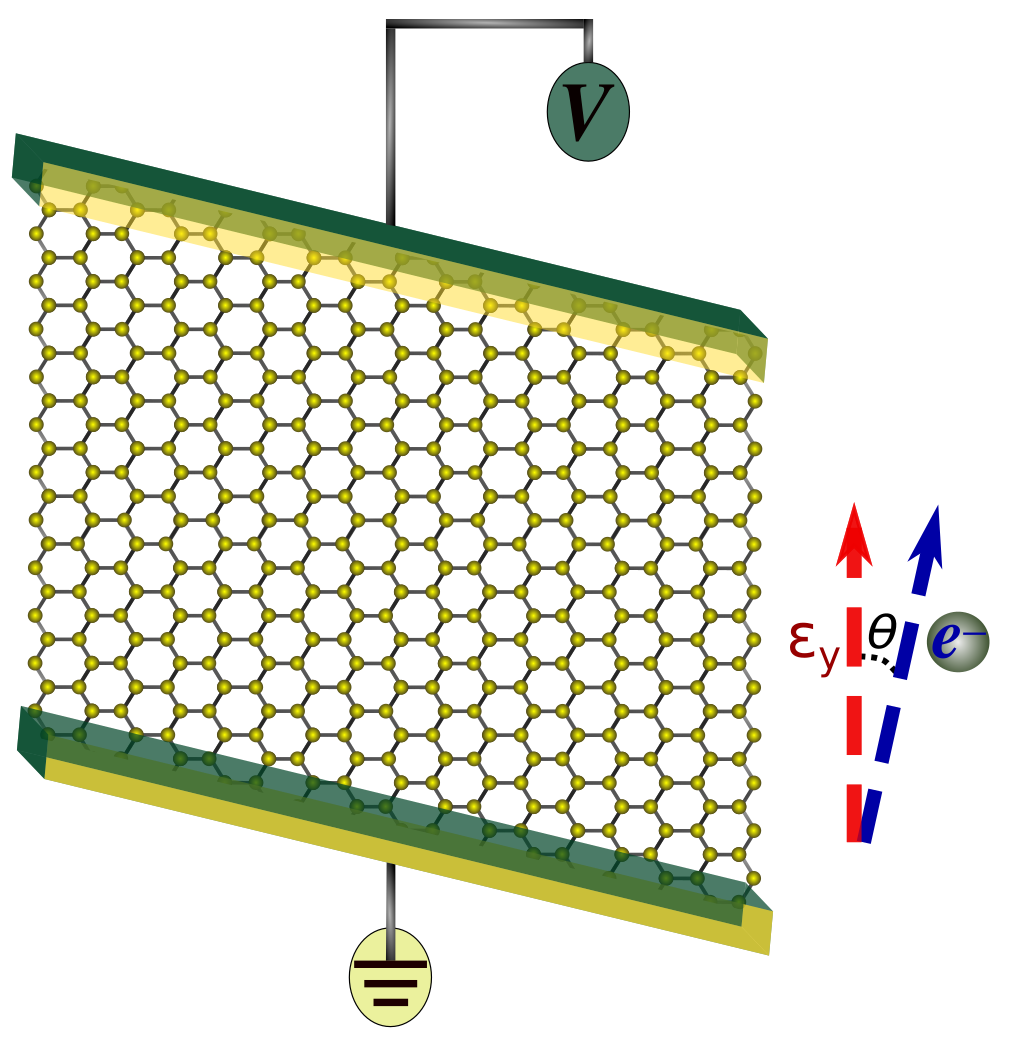
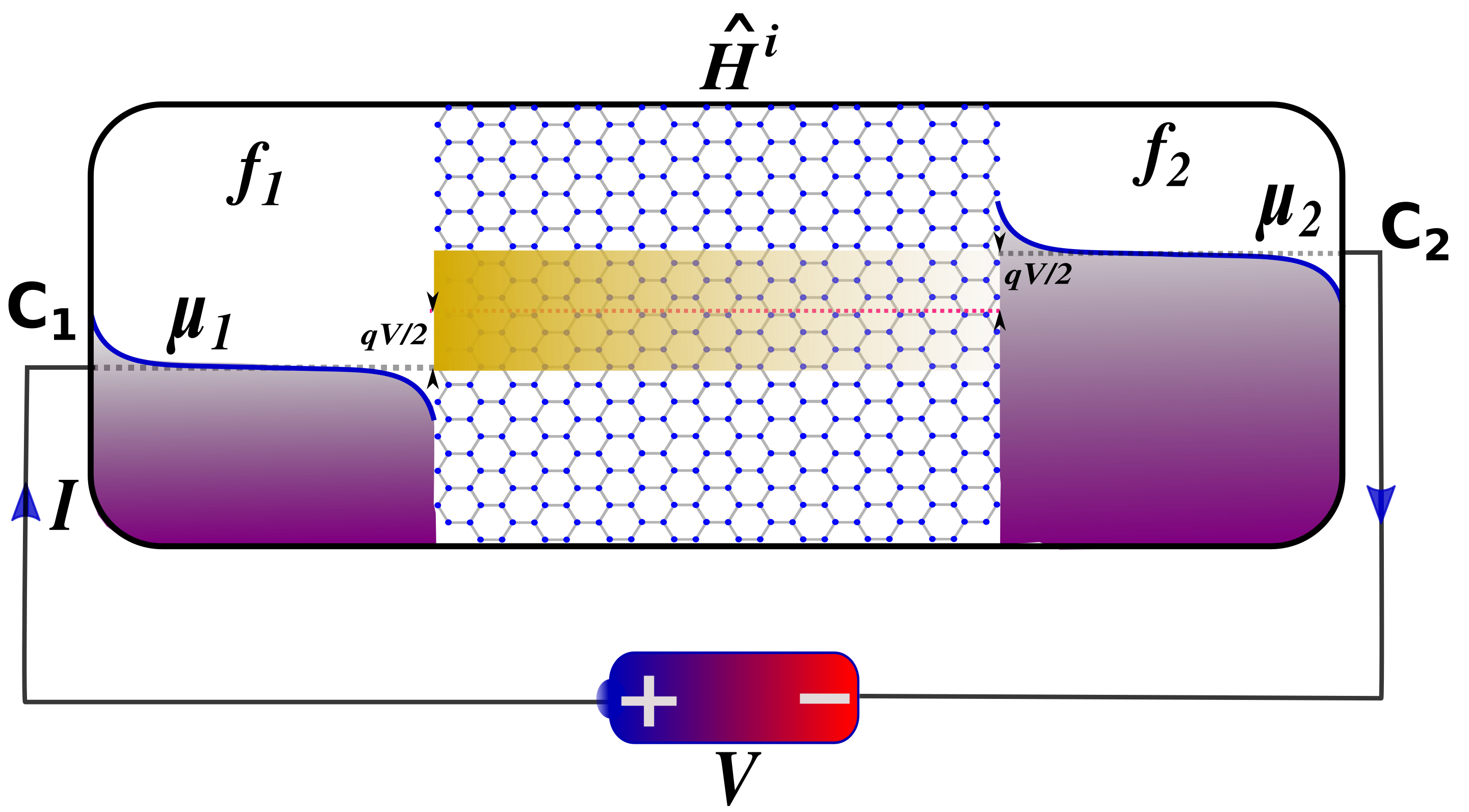
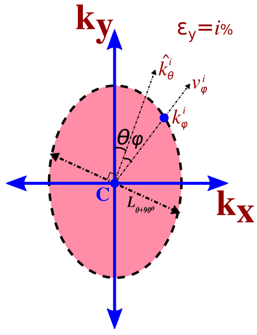
The schematic diagram of the angular gauge factor setup is presented in Fig. 1. A uniaxial strain () is applied along the zigzag direction, and the resistance is computed along different directions represented by ‘’.
The quantum transport model for the given setup is schematized in Fig. 1. The setup constitutes a graphene sheet represented by Hamiltonian ‘’ and ideal reflection-less contacts and . The equilibrium Fermi-energy of the graphene sheet and contacts are maintained at 0 eV. The voltage applied at the terminals and are -V/2 and V/2 Volts respectively.
We note that the simulation setup described here evaluates AGF in the linear regime [-0.01 eV - 0.01eV] within the elastic limit of graphene [].
II.2 Angular gauge factor calculation
The transport properties of graphene in the ballistic regime depends on mode density Datta (2012) whereas in the diffusive regime depends on Fermi velocity Peres et al. (2007). The value of mode density and Fermi-velocity depend on the applied strain. We evaluate the mode density and Fermi velocity of graphene as a function of strain along different directions () from band-structure of strained graphene. The mathematical models derived using quantum transport, and semi-classical transport formalisms for the evaluation of AGF in different transport regimes of graphene are discussed further.
II.2.1 Tight binding model
The tight binding Hamiltonian of a honey-comb lattice is expressed as
| (1) |
In Eq. (1), represents the hopping parameter that connects the lattice site with its neighbours in graphene at strain . and are respectively the annihilation and creation operators of electrons at sites and . We consider that the electron dynamics of graphene is governed by the nearest neighbour tight binding Hamiltonian. Thus, the energy eigen-values of Eq. (1) is given by
| (2) |
where and are the basis vectors of strained graphene, and , and are the nearest neighbor hopping parameters.
We obtain the tight-binding parameters of uniaxially strained graphene from Ribeiro et al. Ribeiro et al. (2009). In Ref. Ribeiro et al. (2009) the parameters are obtained by fitting Eq. 2 with ab-initio band-structures. This model is valid for energy E in the range [-0.2 eV- 0.2 eV].
The nearest neighbor tight binding model of graphene described by Eq. (2) accurately predicts the shift in Dirac cones due to strain, band gap threshold and anisotropy in Fermi velocity Hasegawa et al. (2006); Pereira et al. (2009). This model is consistent with the ab-initio calculations Farjam and Rafii-Tabar (2009); Ribeiro et al. (2009); Choi et al. (2010); Ni et al. (2009); Huang et al. (2011) and experiments Kim et al. (2009); Huang et al. (2010). Thus, Eq. (2) is suitable for AGF calculation in the linear regime.
II.2.2 Ballistic Regime
We compute the current-voltage characteristics of graphene in ballistic regime using Landauer formula which is expressed as
| (3) |
where is the mode density at energy ‘’, strain-percentage ‘’ and electron transport direction ‘’. The resistance calculated from Eq. (3) is expressed as
| (4) |
Thus, the value of AGF in the ballistic regime averaged over the entire strain-limit can be written as
| (5a) | |||
| (5b) | |||
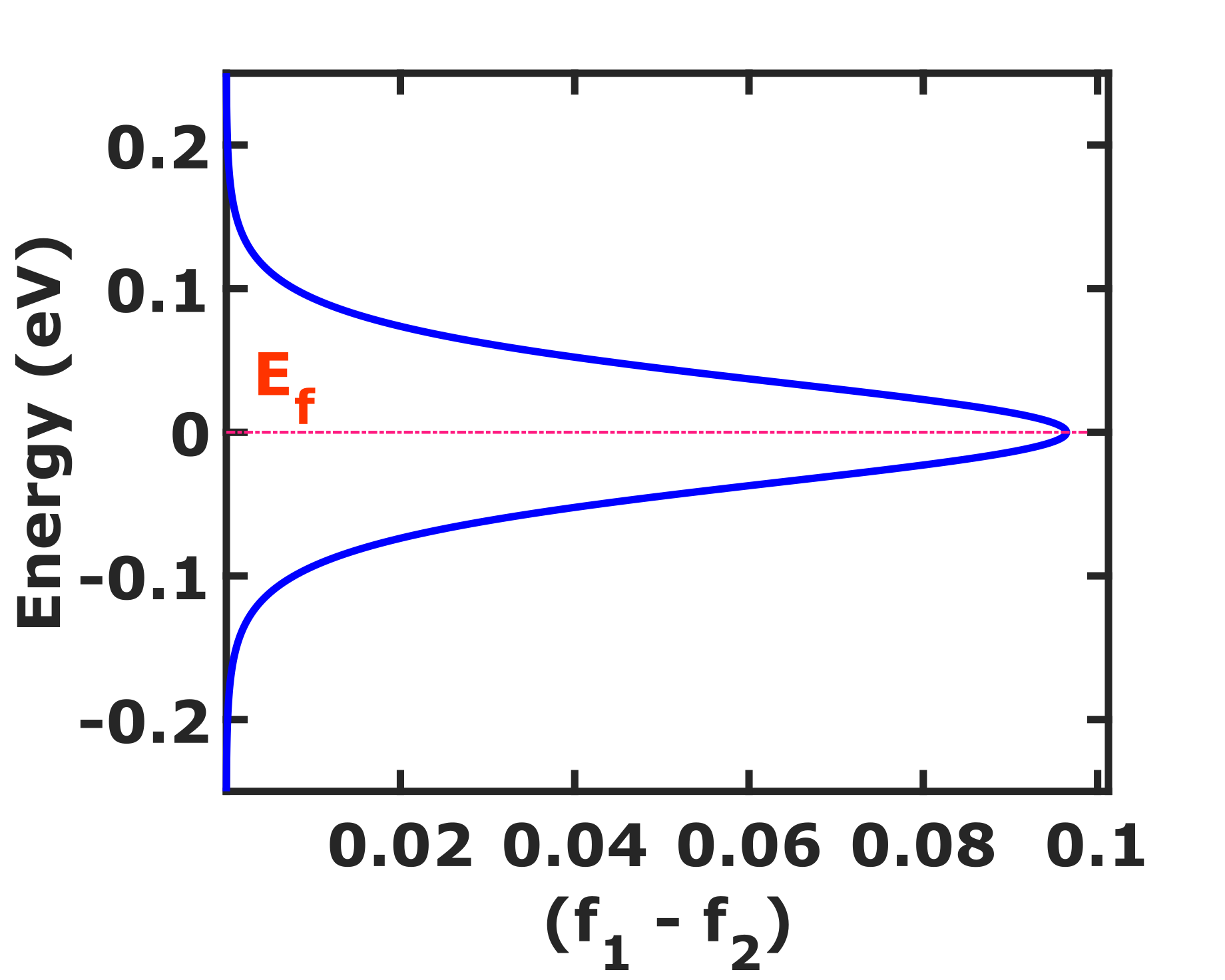
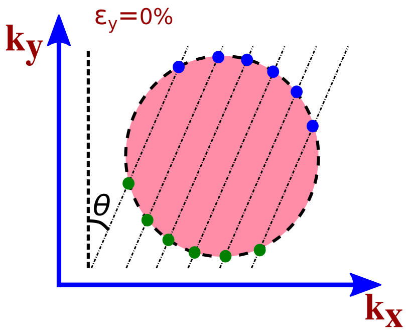
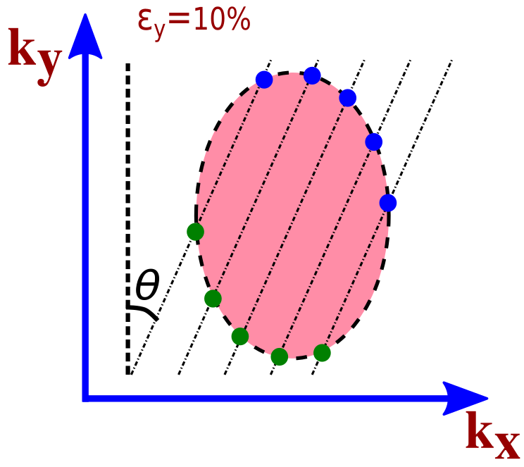
The Fermi-window depends on the energy and applied voltage. We apply a variable potential difference in the range [-0.01 V to 0.01 V] across the contacts. The Fermi-window plot as a function of energy at the potential difference 0.01 V is shown in Fig. 2. The Fermi-window opens up between -0.2 eV to 0.2 eV. Thus, our model using Eqs. (2) and (3) can accurately determine the angular piezo-resistance of graphene in the linear regime.
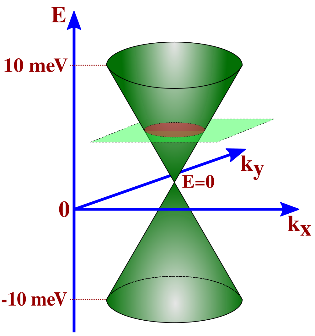
We obtain the mode density ‘’ from the band-structure in Dirac cone approximation. Figure 2 illustrates the constant energy surface formed as a result of intersection of the constant energy plane and the Dirac cone. Figures 2 and 2 illustrate the constant energy surface and modes along at and strain. The blue and green dots represent the modes of forward and backward moving electrons, respectively. Since the effective number of Dirac cones within the first Brillouin zone of strained and unstrained graphene is two Sinha et al. (2019). Thus, the effective number of modes at energy ‘E’ along is numerically equal to the sum of forward and backward moving electrons in a single Dirac cone. The mode density is therefore given by
| (6) |
where is the number of transverse modes (TMs) intersecting the constant energy surface at energy ‘’. The separation between TMs in Figs. 2 and 2 is where is the width of graphene sheet (see Appendix A).
The theoretical model described above for the mode density calculation leads to a significant reduction in the computation-time compared to the full-band mode density calculation Sinha et al. (2019) and can be applied to explore similar applications in other 2D-Dirac materials as well.
| 8.41 | 8.41 | 8.41 | 8.41 | |
| 7.35 | 7.75 | 8.37 | 8.59 | |
| 6.12 | 7.32 | 8.45 | 8.77 |
II.2.3 Diffusive Regime
Electron transport in the diffusive regime is described via the semi-classical transport mechanism. The electrons are treated as classical particles (wave-packets) whose position and momentum are precisely known. The electron mobility determines the electron transport properties in the diffusive regime as compared to mode density in the ballistic regime.
The experimentally determined conductivity of graphene in the diffusive regime shows a linear dependence on electron density except at the charge neutrality point Novoselov et al. (2004). By considering random Coulomb impurities as the dominant source of scattering, a linearly varying conductivity with gate voltage is obtained in Ref. Nomura and MacDonald (2007). The expression for conductivity of graphene as a function of the electron density, considering the presence of charged impurities was formulated using Boltzman transport theory under the relaxation time approximation by Peres et al. The expression for conductivity as derived in Ref. Peres et al. (2007) is given by
| (7) |
The conductivity of graphene in the diffusive regime depends on the electron density and Fermi velocity. However, variation in the conductivity due to a change in electron density is prominent only in the presence of a gate voltage Pereira et al. (2009). In the absence of gate voltage, conductivity depends primarily on the Fermi-velocity. The anisotropy in resistance due to a tensile strain predicted using Eq. (7) comply with the experimental results Kim et al. (2009). Hence, we use Eq. (7) to obtain the expression for AGF in diffusive regime.
The resistance of a uniaxially strained graphene is given by
| (8) |
where , , , and are the resistance, conductivity, length and width respectively at strain ‘’ along the direction ‘’.
Thus, the expression for AGF in the diffusive regime averaged over the entire strain range is given by
| (9a) | |||
| (9b) | |||
The AGF in diffusive regime depends on the variation of Fermi-velocity, electron density, and dimensions of the graphene with strain and direction . The strain-induced variation of Fermi-velocity is discussed in the present section, while the strain-induced change in dimensions is discussed separately in the next sub-section.
The velocity of electrons at an energy close to the Dirac point is equal to its Fermi-velocity. The Fermi-velocity is expressed as
| (10) |
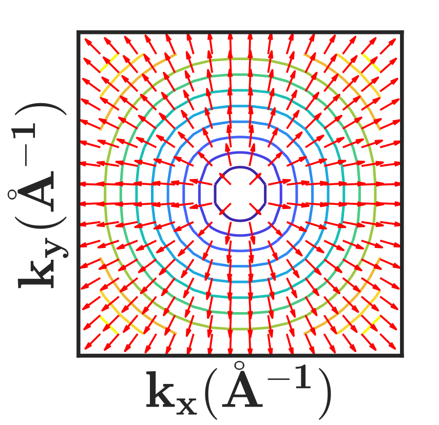
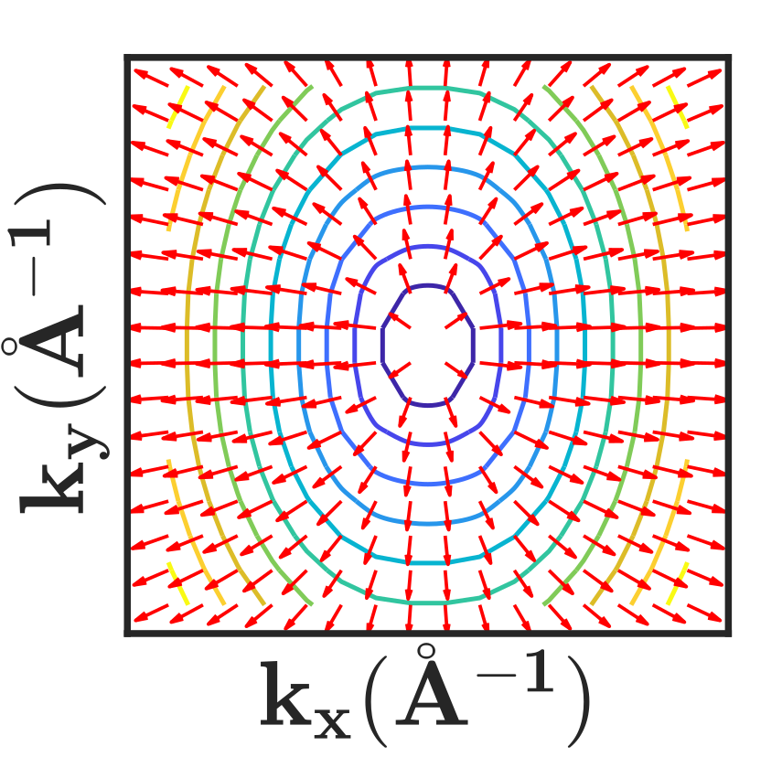
Figures 3 and 3 show the Fermi-velocity vectors and contours near a Dirac point at and strain respectively. The variation in magnitude of Fermi-velocity with and is given in Table 1. From the table, we infer that strain induces anisotropy in the Fermi-velocity. The AGF in diffusive regime depends on the average Fermi-velocity along the direction of transport. Figure 3 illustrates the methodology for evaluation of average Fermi-velocity along the transport direction (). The average Fermi velocity along at strain ‘’ is expressed as
| (11) |
where is the Fermi-velocity along direction and is the unit vector along . See Appendix B for detail derivation of Eq. (11).
II.2.4 Strain distribution in graphene
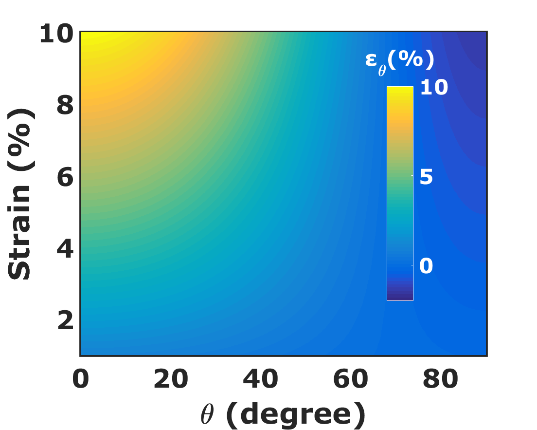
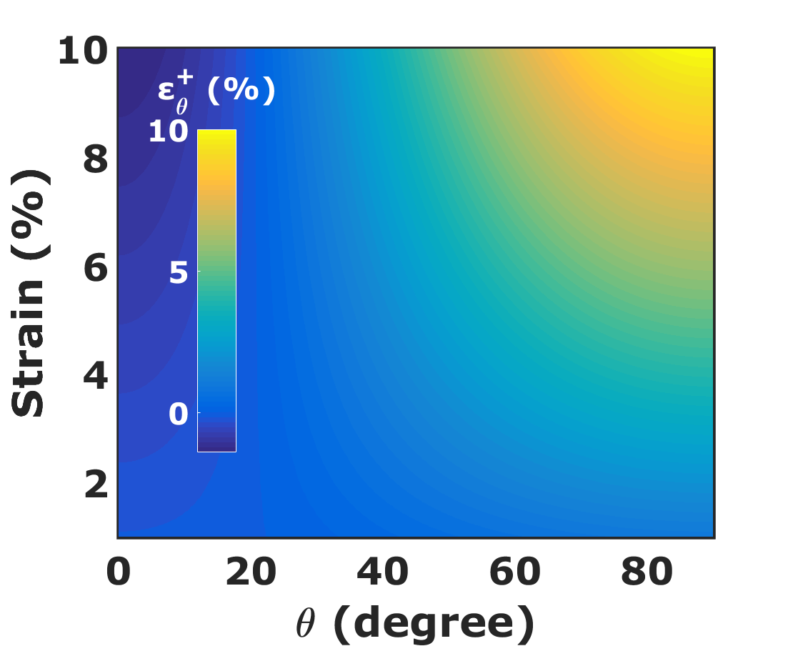
Apart from the variation of Fermi-velocity, AGF also depends on the magnitude of strain along the transport () and transverse directions (). The change in dimensions modifies the mode density and conductivity of graphene (see Eqs. (6) and (9)).
The strain ‘’ generates components along different directions of graphene. The stiffness or compliance matrix due to a uniaxial strain along the basal plane of the graphene sheet is the same irrespective of the choice of coordinate axes Landau (1986). Consequently, the Poisson’s ratio of graphene sheet is the same irrespective of the direction of tensile strain in the basal plane Pereira et al. (2009).
The mean free path of graphene is very high and is in the sub-micron range Adam and Sarma (2008b); Novoselov et al. (2004); Castro Neto et al. (2009). Therefore, we treat graphene as a continuum sheet in strain related calculations in this work.
The strain components along the electron transport direction () and its transverse direction () are expressed as
| (12a) | ||||
| (12b) | ||||
where is the longitudinal strain and is the transverse strain (). In ballistic regime, the mode density depends on the separation between TMs which is given by , where . In diffusive regime, apart from the Fermi-velocity, AGF varies with and (see Eq. 9).
III Results and Discussions


In this section, we obtain the AGF of graphene using the theoretical models discussed earlier and obtain a suitable mathematical fit. We discuss the physics behind the predicted results along with their applications and prospects.
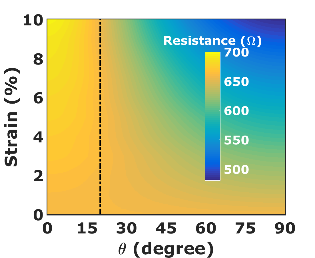
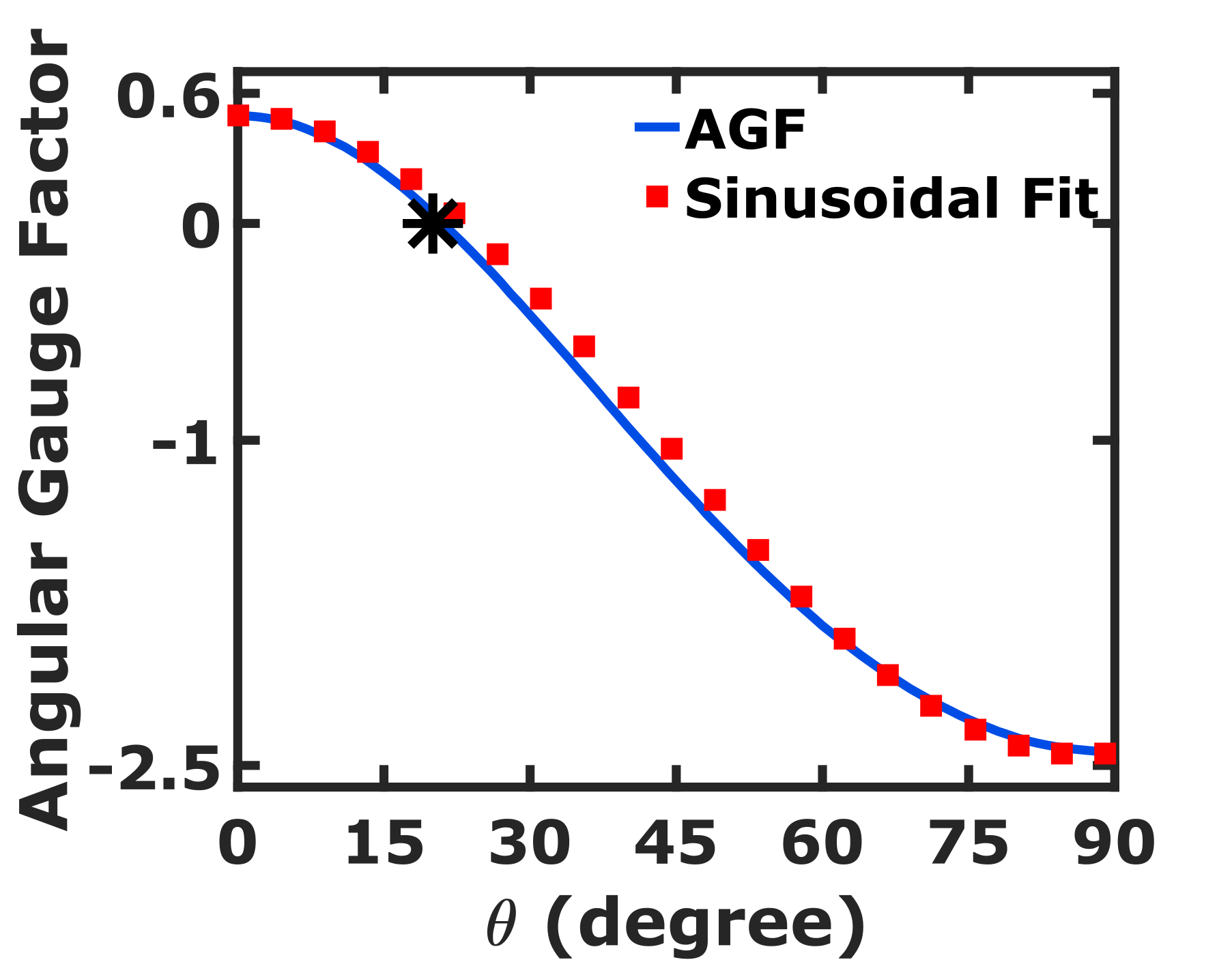
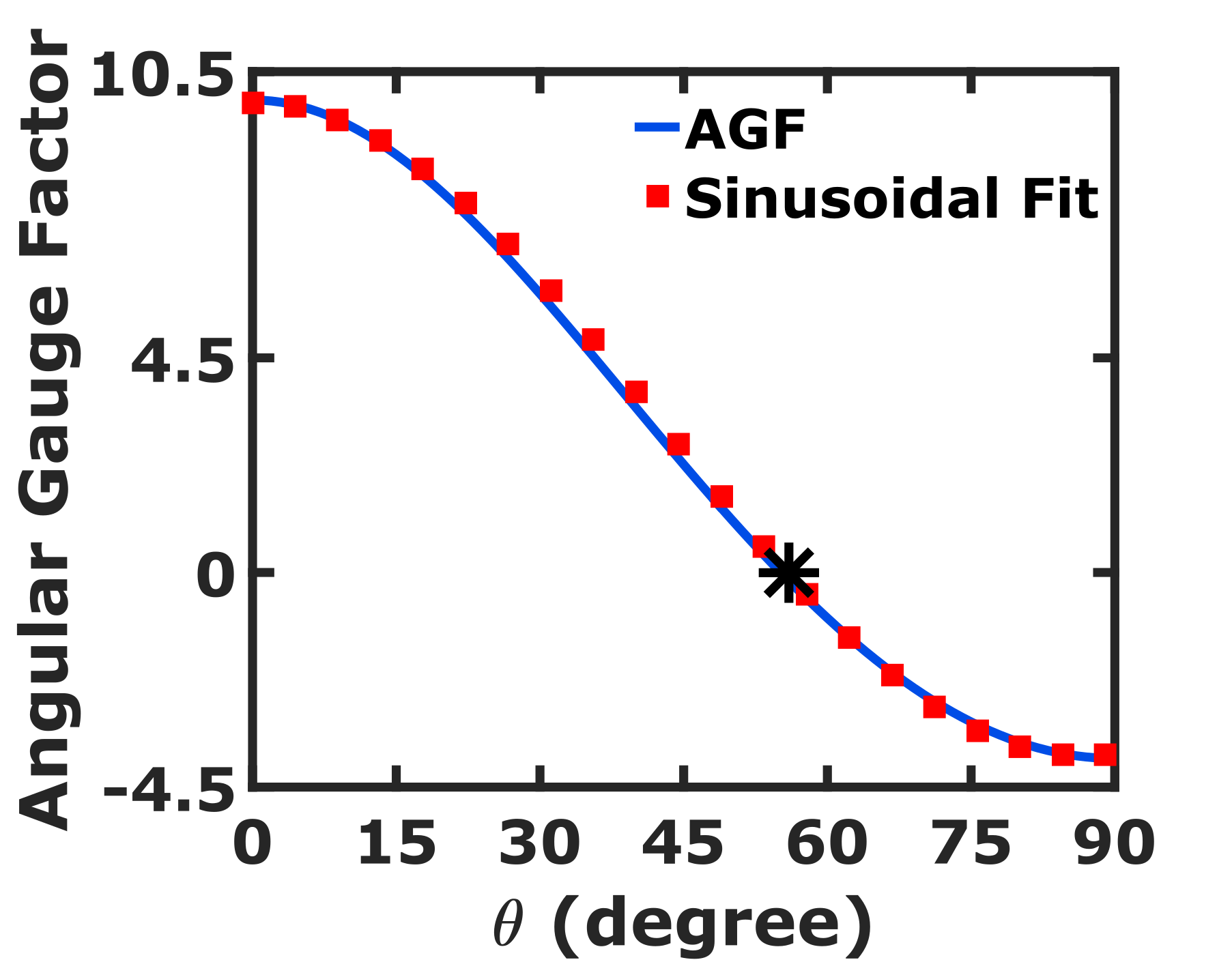
We show in Fig. 4, the variation of resistance of a 1- wide ballistic graphene sheet with and . The resistance at strain is constant irrespective of the direction . Nevertheless, the variation in resistance increases with as increases. Thus, Fig. 4 validates the fact that graphene is electrically isotropic at strain and becomes anisotropic on the application of tensile strain Pereira et al. (2009); Sinha et al. (2019). The anisotropy increases with an increase in strain. The resistance along increases by a small amount with an increase in strain. However, it decreases significantly along with an increase in strain. We note that the resistance remains constant with applied strain at . We show in Fig. 4, the variation of AGF with and the corresponding sinusoidal fit which is a sinusoidal function of the form
| (13) |
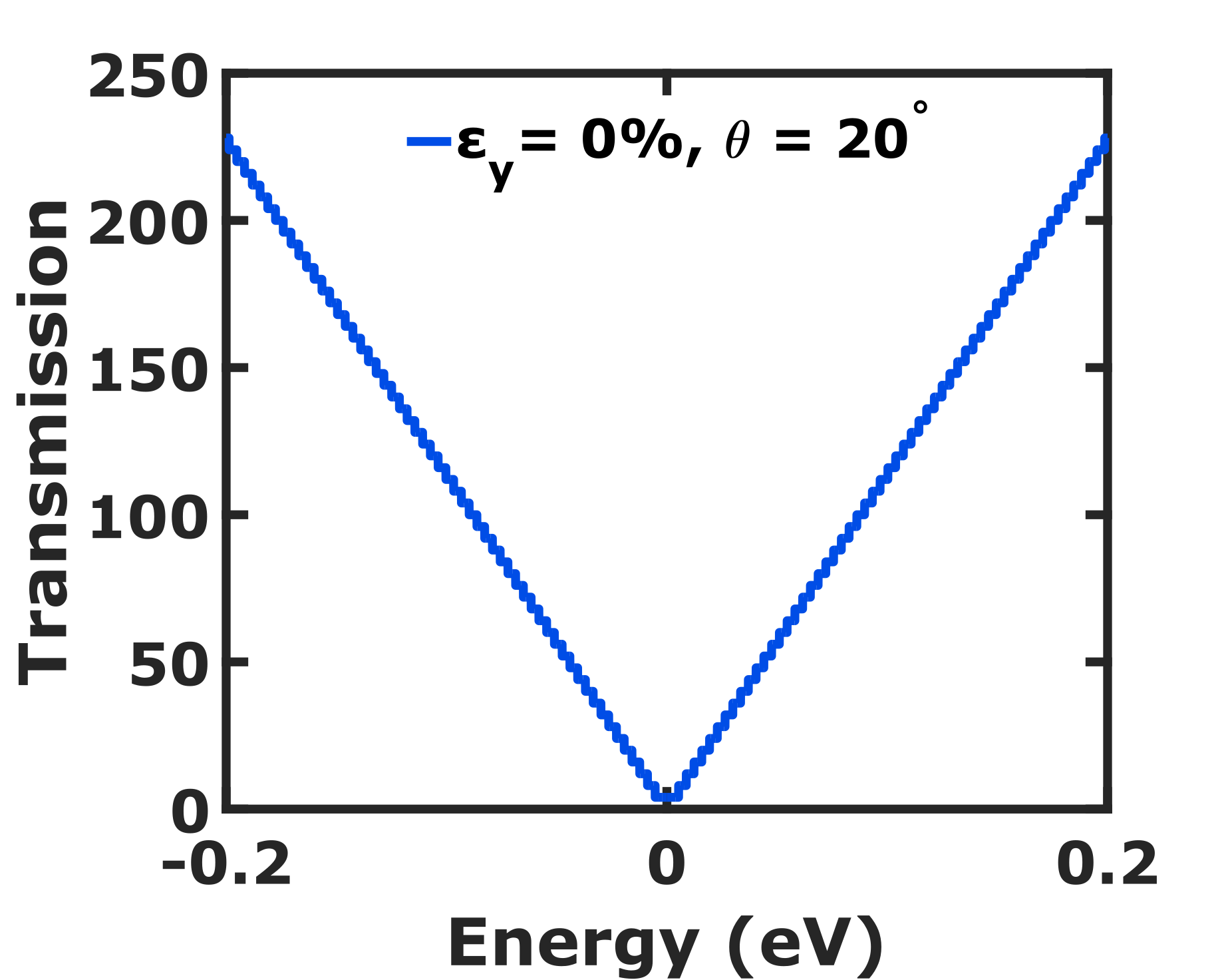
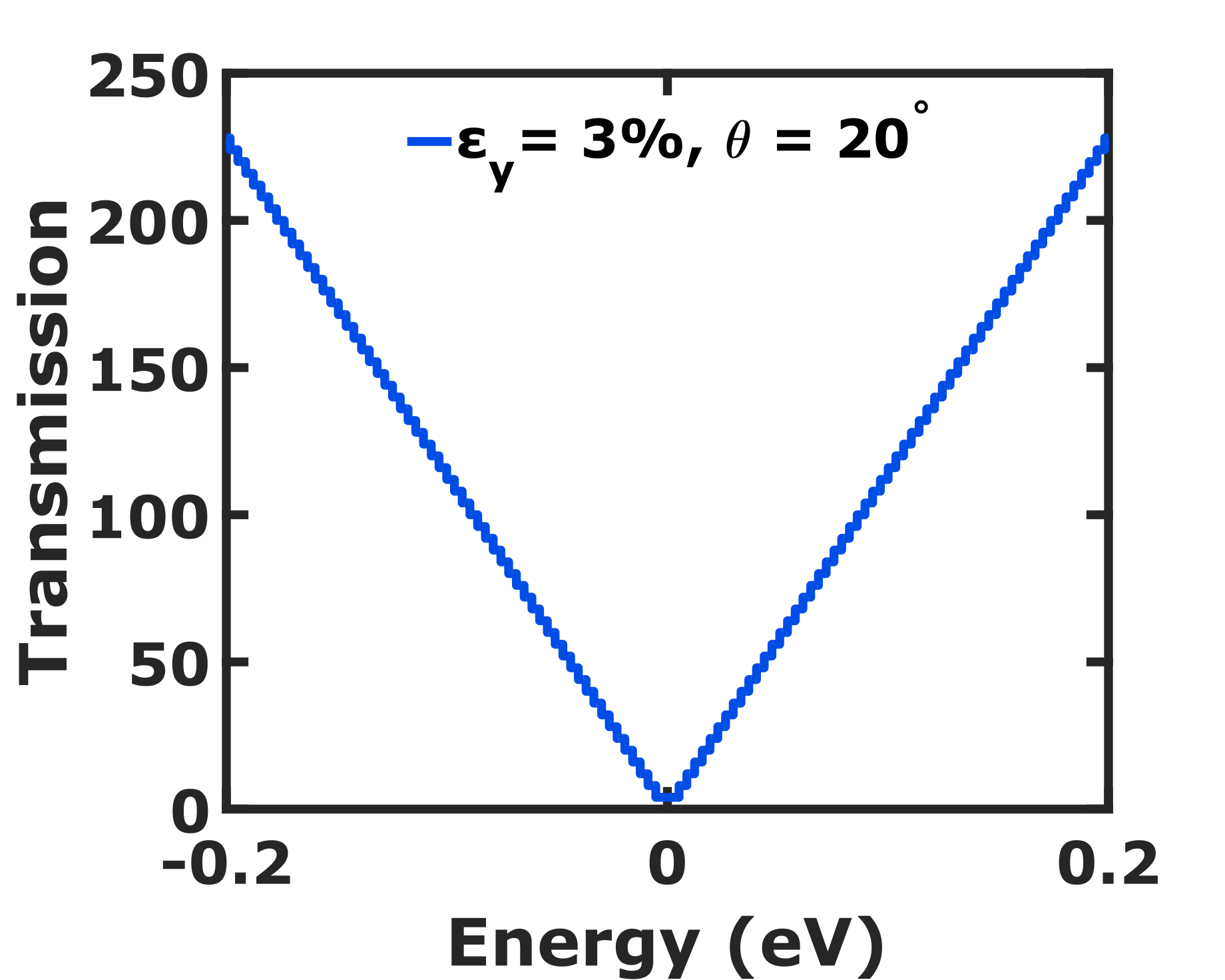
where A = 1.475 and B = -0.975. We see in Fig. 4 that the AGF along , , and are 0.6, 0, and -2.5, respectively. The observed pattern of AGF in the ballistic regime is a result of the deformation of Dirac cone and change in separation of TMs due to strain. The values of AGF at terminal angles and are consistent with the longitudinal and transverse GF of graphene obtained in Ref. Sinha et al. (2019). The transmissions along at different strains are identical as shown in Fig. 5, thereby substantiating our claim of the resistance invariance direction along .
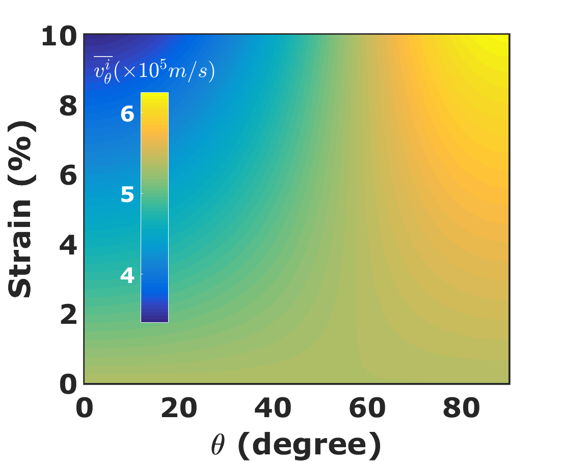
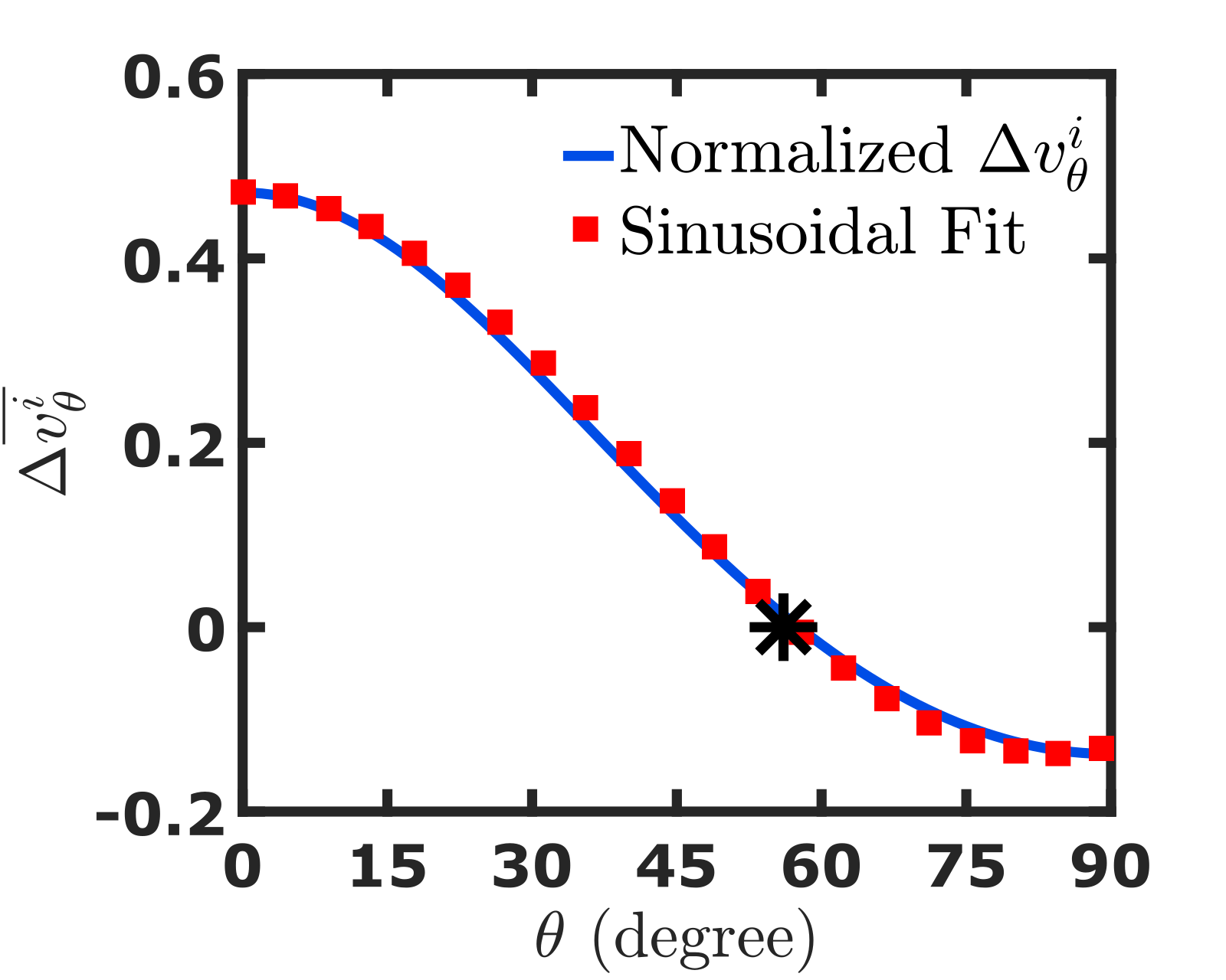
We show in Fig. 6, the variation of average Fermi-velocity with and . The average Fermi-velocity is constant at strain along differnt directions ‘’ and has a magnitude of . The average Fermi-velocity decreases sharply along , becomes zero and finally slightly increases along with the increase in strain. The variation in average Fermi-velocity with and is similar to the variation of Fermi-velocity (see Table 1). Figures 6 and 6 depict and as a function of and . The color maps of and are mirror image of each other due to two-fold symmetry and isotropic nature of a uniaxially strained graphene (explained in the next paragraph).
Figure 6 presents the AGF in diffusive graphene. The plot of AGF with can be approximated by a sinusoidal curve given by
| (14) |
where C = 6.85 and D = 3. The value of AGF varies sinusoidally between 9.85 to -3.85 and is zero at in the diffusive regime. We see that ballistic graphene has higher GF along whereas diffusive graphene has higher GF along .
Graphene has a six-fold symmetry, but due to the application of tensile strain, its symmetry reduces into a two-fold symmetry. In Figs. 4 and 6, the AGF plots have a periodicity of ‘’ which is due to the two-fold symmetry of uniaxially strained graphene lattice.
The results obtained in this paper are for a strain applied along the zigzag direction. Nevertheless, the results are same for strain along the armchair direction due to the isotropic Poisson’s ratio Pereira et al. (2009) and identical deformation of the Dirac cone for strain along with armchair and zigzag directions Sinha et al. (2019). The explanation for sinusoidal AGF and the application of these results are discussed in the subsequent sections of this paper.
III.1 Physics of sinusoidal AGF
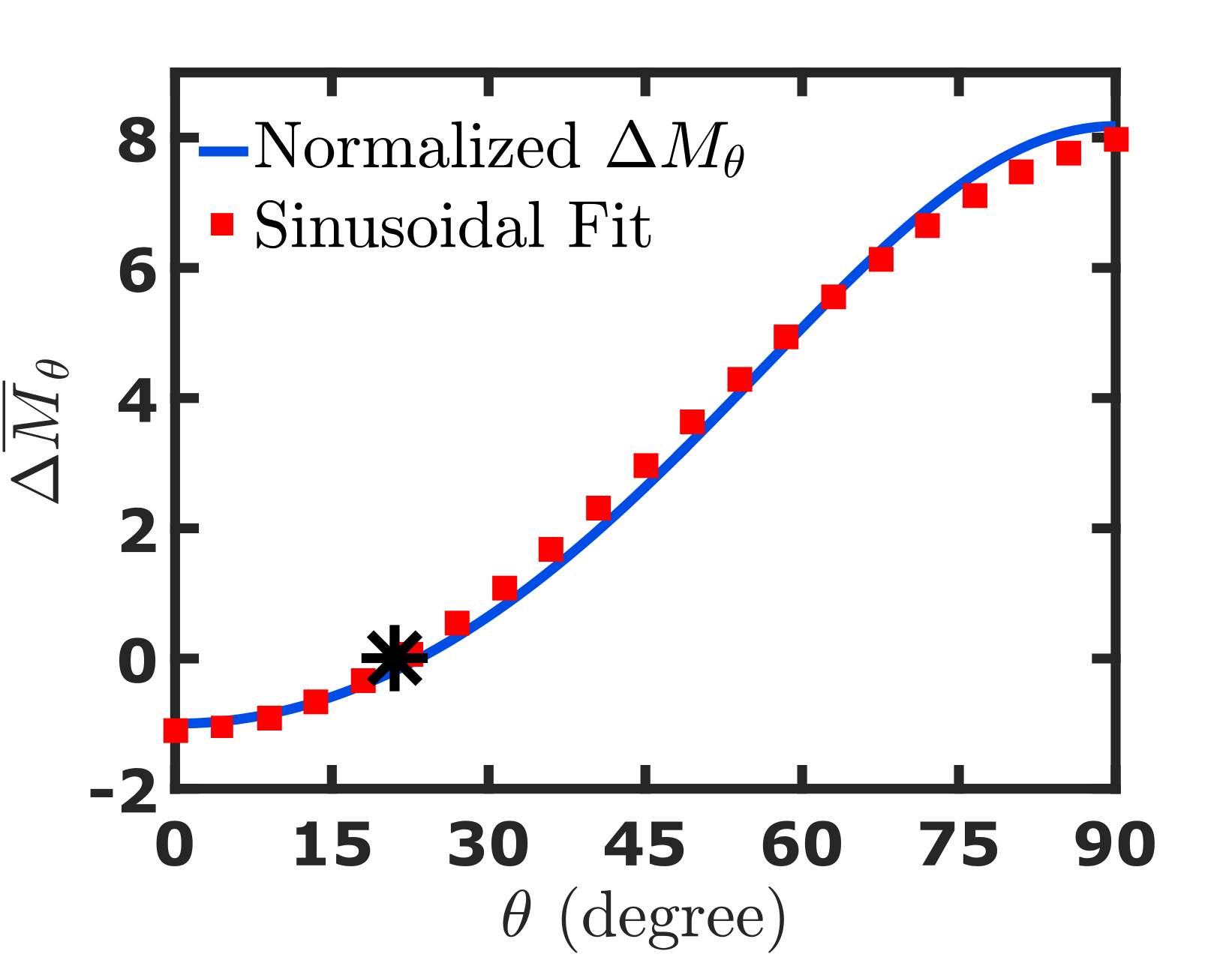
The mode density along a transport angle changes as a result of the applied strain due to the deformation of Dirac cone Sinha et al. (2019). The change in mode density is inversely proportional to the change in normalized resistance along the transport angle . In other words, AGF is inversely proportional to the change in normalized mode density. The mode density and change in the normalized mode density averaged over the entire strain range [] is mathematically expressed as
| (15a) | |||
| (15b) | |||
where , and are respectively the mode density, width of the graphene sheet and length of the axis of Dirac cone along the transverse direction as shown in Fig. 3. We show in Fig. 7, the plot of represented by Eq. 15b. Figure 7 is similar to the reciprocal of AGF in Fig. 4. Thus, the sinusoidal nature of AGF in ballistic graphene is due to the sinusoidal variation of mode density along different .
The AGF in diffusive graphene depends on the average Fermi-velocity along , strain along the transport direction() and the transverse direction (). Table 2 shows the variation of these parameters at transport angles , and . From the table, we infer that among these parameters, the contribution of average Fermi-velocity in the AGF supersedes all other parameters. We show in Fig. 7, the variation of average Fermi-velocity with is similar to a sinusoidal function and resembles the AGF in diffusive regime. Thus, the sinusoidal variation of AGF with transport angle is due to the sinusoidal variation of average Fermi-velocity with transport angle .
| 0.52 | 0.055 | 0.008 | |
| 0.13 | 0.024 | -0.024 | |
| -0.15 | -0.008 | -0.055 |
III.2 Application and future scope
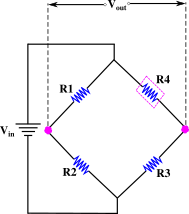
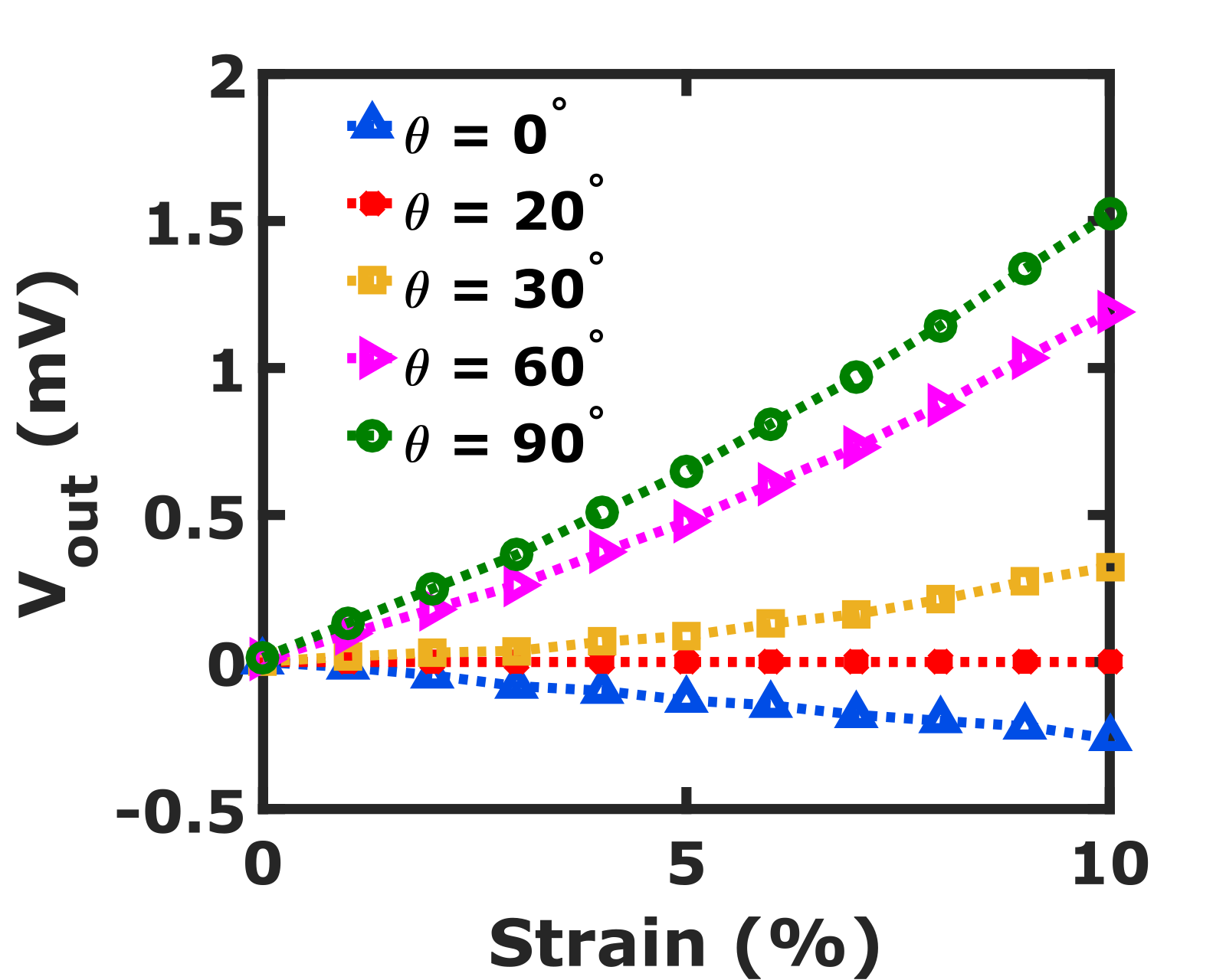
Piezoresistance sensing is commonly done using the Wheatstone bridge readout technique. We show in Fig. 8, a Wheatstone bridge based piezoresistance sensing setup for ballistic graphene. The Wheatstone bridge consists of identical ballistic graphene resistors ,, and . At zero strain, the resistors are equal, and the bridge is in a balanced state. is the strain sensor, and the other resistors act as reference resistors. When subjected to strain, the resistance of changes, which results in the generation of a potential difference (), as shown in Fig. 8. Figure 8 shows versus strain for different values of when the input voltage is maintained at 0.02 eV. is highest when . In addition, shows a linear dependence with strain at different . Thus, ballistic graphene can act as a strain sensor and shows maximum sensitivity at . Ballistic graphene can be used to detect explosives, gases, etc. provided the strain generated is mapped with the vapor density of explosives or gases. Boisen et al. (2011); Seena et al. (2011); Nelson et al. (2006); Pinnaduwage et al. (2004).
A major problem pertaining to the strain sensor is the presence of an inherent residual strain. Consequently, is non-zero even when no external strain is applied. In fact, during explosive detection or chemical sensing, the reference sensors are vulnerable to unwanted strain by the vapors of explosives and gases Boisen et al. (2011); Seena et al. (2011); Nelson et al. (2006); Pinnaduwage et al. (2004). In this paper, we propose a solution to overcome this problem without removing the residual or unwanted strain. As discussed earlier, the AGF of ballistic and diffusive graphene is zero at the critical angles. In this direction, the resistance does not change even in the presence of strain. The resistance along the critical angle is always equal to the resistance along any other direction at strain. The above discussion is equally valid for diffusive graphene also. Hence, we propose a graphene-based reference piezoresistor with the transport along the critical angle in the Wheatstone bridge read-out technique.
Due to the excellent electro-mechanical properties, graphene is also a strong contender for materials used in flexible electronics Kim et al. (2009); Sharma and Ahn (2013). The critical angle may find application in future flexible devices where a constant current is required despite the presence of a variable strain.
The existence of a critical angle in ballistic graphene is due to the unique deformation pattern of Dirac cone as a result of applied uniaxial strain. Similar studies for 2-D Dirac materials such as Silicene and Germanene etc. in ballistic regimes can be undertaken for similar applications in the future.
IV Conclusion
In summary, we investigated the angular gauge factor of graphene in the ballistic and diffusive regimes using highly efficient quantum transport models. It was shown that the angular gauge factor in both ballistic and diffusive graphene between to bears a sinusoidal relation with a periodicity of due to the reduction of six-fold symmetry into a two-fold symmetry as a result of applied strain. The angular gauge factor is zero at critical angles and in ballistic and diffusive regimes, respectively. Based on these findings, we propose a graphene-based ballistic nano-sensor, which can be used as a reference piezoresistor in a Wheatstone bridge read-out technique. The reference sensors proposed here are unsusceptible to inherent residual strain present in strain sensors and unwanted strain generated by the vapors in explosives detection. The theoretical models developed in this paper can be applied to explore similar applications in other 2D-Dirac materials. The proposals made here potentially pave the way for implementation of NEMS strain sensors based on the principle of ballistic transport, which will eventually replace MEMS piezoresistance sensors with a decrease in feature size. The presence of strain insensitive “critical angle” in graphene may be useful in flexible wearable electronics also.
Acknowledgements.
The Research and Development work undertaken in the project under the Visvesvaraya Ph.D. Scheme of Ministry of Electronics and Information Technology, Government of India, is implemented by Digital India Corporation (formerly Media Lab Asia). This work was also supported by the Science and Engineering Research Board (SERB), Government of India, Grant No. EMR/2017/002853 and Grant No. STR/2019/000030 and the Ministry of Human Resource and Development (MHRD), Government of India, Grant no. STARS/APR2019/NS/226/FS under the STARS scheme. The author Abhinaba Sinha was also supported by NNETRA project under Sanction Order: DST/NM/NNetRA/2018(G)-IIT-B at IIT Bombay.Appendix A Separation between adjacent transverse modes
The separation between adjacent states of conduction electrons in reciprocal space is determined by periodic boundary condition Ashcroft et al. (2016). Electrons in conduction band behave as nearly free electrons. The wave-function of these electrons are expressed as
| (16) |
Equation (16) represents a plane-wave equation travelling along . Let us consider a crystal of length L and wave-function at r=0 and r=L be denoted by and respectively. The wave-functions at the boundaries are equal as a result of periodic boundary condition. Thus,
| (17) |
Using Eqs. (16) and (17), we obtain the allowed states which is expressed as
| (18) |
where n=0,1,2,3…..
The separation between -states in reciprocal space is , where L is the length of the crystal. Extending the same reasoning along the width (w), we obtain a separation of between adjacent transverse modes (TMs) along the width in reciprocal space.
Appendix B Average Fermi-velocity under Dirac cone approximation
Under the Dirac cone approximation, the velocity of electrons along at different energies are equal to the Fermi-velocity (see Fig. 3). The magnitude of Fermi-velocity along different directions are equal in unstrained graphene. Application of a tensile strain () results in anisotropic Fermi-velocity (see Fig. 3). As a result, evaluation of the conductivity of strained graphene using Eq. (7) will require the value of average Fermi-velocity along .
Figure 3 illustrates the methodology for calculating average Fermi-velocity. The direction of Fermi velocity() forming angle in the range to with respect to have velocity components along . The Fermi-velocity () along is expressed as
| (19) |
The component of along is , where is a unit-vector along . Thus, the mean of these components for different values of along is given by
| (20) |
References
- Madou (2003) M. Madou, in Symposium on Design, Test, Integration and Packaging of MEMS/MOEMS 2003. (2003) p. 1.
- Wang and Soper (2006) W. Wang and S. A. Soper, Bio-MEMS: technologies and applications (CRC press, 2006).
- Tsai and Sue (2007) N.-C. Tsai and C.-Y. Sue, Sensors and Actuators A: Physical 134, 555 (2007).
- Kleinstreuer et al. (2008) C. Kleinstreuer, J. Li, and J. Koo, International Journal of Heat and Mass Transfer 51, 5590 (2008).
- Jang and Liccardo (2007) J. S. Jang and D. Liccardo, IEEE Aerospace and Electronic Systems Magazine 22, 30 (2007).
- Leclerc (2007) J. Leclerc, IEEE Aerospace and Electronic Systems Magazine 22, 31 (2007).
- Desai et al. (1999) A. Desai, S.-W. Lee, and Y.-C. Tai, Sensors and Actuators A: Physical 73, 37 (1999).
- Tang and Lee (2001) W. C. Tang and A. P. Lee, Mrs Bulletin 26, 318 (2001).
- Siepmann (2006) J. P. Siepmann, in Laser Radar Technology and Applications XI, Vol. 6214 (International Society for Optics and Photonics, 2006) p. 621409.
- Nam and Lee (2005) Y.-W. Nam and S.-h. Lee, “Flexible mems transducer and manufacturing method thereof, and flexible mems wireless microphone,” (2005), uS Patent 6,967,362.
- Mcneil et al. (2005) A. C. Mcneil, G. Li, and D. N. Koury Jr, “Single proof mass, 3 axis mems transducer,” (2005), uS Patent 6,845,670.
- Rebeiz and Muldavin (2001) G. M. Rebeiz and J. B. Muldavin, IEEE Microwave magazine 2, 59 (2001).
- Brown (1998) E. R. Brown, IEEE Transactions on microwave theory and techniques 46, 1868 (1998).
- Tsai et al. (2008) C.-Y. Tsai, W.-T. Kuo, C.-B. Lin, and T.-L. Chen, Journal of Micromechanics and Microengineering 18, 045001 (2008).
- Tsai and Chen (2010) C.-Y. Tsai and T.-L. Chen, Journal of Micromechanics and Microengineering 20, 095021 (2010).
- Bell et al. (2005) D. J. Bell, T. Lu, N. A. Fleck, and S. M. Spearing, Journal of Micromechanics and Microengineering 15, S153 (2005).
- Conway et al. (2007) N. J. Conway, Z. J. Traina, and S.-G. Kim, Journal of Micromechanics and Microengineering 17, 781 (2007).
- Reeds III et al. (2003) J. W. Reeds III, Y. W. Hsu, and P. C. Dao, “Mems sensor with single central anchor and motion-limiting connection geometry,” (2003), uS Patent 6,513,380.
- Kitano et al. (2006) M. Kitano, H. Sumi, and T. Moribe, “Capacitance difference detecting circuit and mems sensor,” (2006), uS Patent 7,119,550.
- Liu et al. (2007) F. Liu, P. Ming, and J. Li, Phys. Rev. B 76, 064120 (2007).
- Kim et al. (2009) K. S. Kim, Y. Zhao, H. Jang, S. Y. Lee, J. M. Kim, K. S. Kim, J.-H. Ahn, P. Kim, J.-Y. Choi, and B. H. Hong, Nature 457, 706 (2009).
- Lee et al. (2008) C. Lee, X. Wei, J. W. Kysar, and J. Hone, Science 321, 385 (2008).
- Novoselov et al. (2004) K. S. Novoselov, A. K. Geim, S. V. Morozov, D. Jiang, Y. Zhang, S. V. Dubonos, I. V. Grigorieva, and A. A. Firsov, Science 306, 666 (2004).
- Adam and Sarma (2008a) S. Adam and S. D. Sarma, Solid State Communications 146, 356 (2008a).
- Castro Neto et al. (2009) A. H. Castro Neto, F. Guinea, N. M. R. Peres, K. S. Novoselov, and A. K. Geim, Rev. Mod. Phys. 81, 109 (2009).
- Smith et al. (2013) A. Smith, F. Niklaus, A. Paussa, S. Vaziri, A. C. Fischer, M. Sterner, F. Forsberg, A. Delin, D. Esseni, P. Palestri, et al., Nano letters 13, 3237 (2013).
- Dolleman et al. (2015) R. J. Dolleman, D. Davidovikj, S. J. Cartamil-Bueno, H. S. van der Zant, and P. G. Steeneken, Nano letters 16, 568 (2015).
- Wang et al. (2016) Q. Wang, W. Hong, and L. Dong, Nanoscale 8, 7663 (2016).
- Li et al. (2018) Y. Li, H. Yu, X. Qiu, T. Dai, J. Jiang, G. Wang, Q. Zhang, Y. Qin, J. Yang, and X. Jiang, Scientific Reports 8, 1562 (2018).
- Chen et al. (2009) C. Chen, S. Rosenblatt, K. I. Bolotin, W. Kalb, P. Kim, I. Kymissis, H. L. Stormer, T. F. Heinz, and J. Hone, Nature nanotechnology 4, 861 (2009).
- Huang et al. (2012) Y. Huang, J. Liang, and Y. Chen, J. Mater. Chem. 22, 3671 (2012).
- Rogers and Liu (2011) G. W. Rogers and J. Z. Liu, Journal of the American Chemical Society 133, 10858 (2011).
- Datta (2012) S. Datta, “Lessons from nanoelectronics: A new perspective on transport.–hackensack,” (2012).
- Patil and Muralidharan (2017) U. Patil and B. Muralidharan, Physica E: Low-dimensional Systems and Nanostructures 85, 27 (2017).
- Priyadarshi et al. (2018) P. Priyadarshi, A. Sharma, S. Mukherjee, and B. Muralidharan, Journal of Physics D: Applied Physics 51, 185301 (2018).
- Mukherjee et al. (2018) S. Mukherjee, P. Priyadarshi, A. Sharma, and B. Muralidharan, IEEE Transactions on Electron Devices 65, 1896 (2018).
- Singh et al. (2018) S. Singh, K. Thakar, N. Kaushik, B. Muralidharan, and S. Lodha, Phys. Rev. Applied 10, 014022 (2018).
- Singha and Muralidharan (2017) A. Singha and B. Muralidharan, Scientific Reports 7, 7879 (2017).
- Singha and Muralidharan (2018) A. Singha and B. Muralidharan, Journal of Applied Physics 124, 144901 (2018).
- Sinha et al. (2019) A. Sinha, A. Sharma, A. Tulapurkar, V. R. Rao, and B. Muralidharan, Phys. Rev. Materials 3, 124005 (2019).
- Huang et al. (2011) M. Huang, T. A. Pascal, H. Kim, W. A. Goddard, and J. R. Greer, Nano Letters 11, 1241 (2011).
- Smith et al. (2016) A. D. Smith, F. Niklaus, A. Paussa, S. Schröder, A. C. Fischer, M. Sterner, S. Wagner, S. Vaziri, F. Forsberg, D. Esseni, M. Östling, and M. C. Lemme, ACS Nano 10, 9879 (2016).
- Mawrie and Muralidharan (2019a) A. Mawrie and B. Muralidharan, Phys. Rev. B 99, 075415 (2019a).
- Mawrie and Muralidharan (2019b) A. Mawrie and B. Muralidharan, Phys. Rev. B 100, 081403 (2019b).
- Peres et al. (2007) N. M. R. Peres, J. M. B. Lopes dos Santos, and T. Stauber, Phys. Rev. B 76, 073412 (2007).
- Ribeiro et al. (2009) R. M. Ribeiro, V. M. Pereira, N. M. R. Peres, P. R. Briddon, and A. H. C. Neto, New Journal of Physics 11, 115002 (2009).
- Hasegawa et al. (2006) Y. Hasegawa, R. Konno, H. Nakano, and M. Kohmoto, Phys. Rev. B 74, 033413 (2006).
- Pereira et al. (2009) V. M. Pereira, A. H. Castro Neto, and N. M. R. Peres, Phys. Rev. B 80, 045401 (2009).
- Farjam and Rafii-Tabar (2009) M. Farjam and H. Rafii-Tabar, Phys. Rev. B 80, 167401 (2009).
- Choi et al. (2010) S.-M. Choi, S.-H. Jhi, and Y.-W. Son, Phys. Rev. B 81, 081407 (2010).
- Ni et al. (2009) Z. H. Ni, T. Yu, Y. H. Lu, Y. Y. Wang, Y. P. Feng, and Z. X. Shen, ACS Nano 3, 483 (2009).
- Huang et al. (2010) M. Huang, H. Yan, T. F. Heinz, and J. Hone, Nano Letters 10, 4074 (2010).
- Nomura and MacDonald (2007) K. Nomura and A. H. MacDonald, Phys. Rev. Lett. 98, 076602 (2007).
- Landau (1986) L. Landau, Course of theoretical physics 7 (1986).
- Adam and Sarma (2008b) S. Adam and S. D. Sarma, Solid State Communications 146, 356 (2008b).
- Boisen et al. (2011) A. Boisen, S. Dohn, S. S. Keller, S. Schmid, and M. Tenje, Reports on Progress in Physics 74, 036101 (2011).
- Seena et al. (2011) V. Seena, A. Fernandes, P. Pant, S. Mukherji, and V. R. Rao, Nanotechnology 22, 295501 (2011).
- Nelson et al. (2006) I. C. Nelson, D. Banerjee, W. J. Rogers, and M. S. Mannan, in Micro (MEMS) and Nanotechnologies for Space Applications, Vol. 6223 (International Society for Optics and Photonics, 2006) p. 62230O.
- Pinnaduwage et al. (2004) L. Pinnaduwage, A. Wig, D. Hedden, A. Gehl, D. Yi, T. Thundat, and R. Lareau, Journal of Applied Physics 95, 5871 (2004).
- Sharma and Ahn (2013) B. K. Sharma and J.-H. Ahn, Solid-State Electronics 89, 177 (2013).
- Ashcroft et al. (2016) N. W. Ashcroft, N. D. Mermin, and D. Wei, Solid State Physics (Cengage Learning Asia Pte Limited, 2016).