[S-]SI_PRB
Proximity effect in a superconductor-topological insulator heterostructure based on first principles
Abstract
Superconductor-topological insulator (SC-TI) heterostructures were proposed to be a possible platform to realize and control Majorana zero-modes. Despite experimental signatures indicating their existence, univocal interpretation of the observed features demands theories including realistic electronic structures. To achieve this, we solve the Kohn-Sham-Dirac-Bogoliubov-de Gennes equations for ultrathin Bi2Se3 films on superconductor PdTe, within the fully relativistic Korringa-Kohn-Rostoker method, and investigate quasiparticle spectra as a function of chemical potential and film thickness. We find a strongly momentum-dependent proximity-induced gap feature where the gap sizes highly depend on characteristics of the TI states. The interface TI Dirac state is relevant to the induced gap only when the chemical potential is close to the Dirac-point energy. Otherwise, at a given chemical potential, the largest induced gap arises from the highest-energy quantum-well states, whereas the smallest gap arises from the TI topological surface state with its gap size depending on the TI pairing potential.
I Introduction
Superconducting proximity effects in nanoscale heterostructures have been studied in various experimental platforms since proposals Kitaev (2001); Fu and Kane (2008); Alicea (2012) on realization of Majorana zero-modes in them. Representative systems are superconductor(SC)-topological insulator(TI) heterostructures Yang et al. (2012); Wang et al. (2012); Xu et al. (2014a, b); He et al. (2014); Xu et al. (2015); Flototto et al. (2018); Sun et al. (2017) and semiconductor nanowires or ferromagnetic chains on SC substrates Mourik et al. (2012); Gül et al. (2017); Zhang et al. (2018); Nadj-Perge et al. (2014); Feldman et al. (2017); Ruby et al. (2017); Palacio-Morales et al. (2019). Majorana zero modes remain robust over local environmental perturbations due to the topological nature, which allows their applications to quantum computation Kitaev (2003). Experimental data has exhibited signatures of Majorana zero modes, yet there remains debate on whether other possibilities can be completely excluded for them. This doubt is raised from inconsistent experimental findings and current theoretical limitations.
In SC-TI heterostructures, it was predicted that the topological TI interface state creates proximity-induced topological superconductivity where the edge state or the vortex lattice can host Majorana zero-modes. Keeping this in mind, experiments were performed on Bi2Se3(111) or Bi2Te3(111) films ( 10 nm) grown on NbSe2 or Nb substrates, using scanning tunneling miscroscopy/spectroscopy (STM/S) Wang et al. (2012); Xu et al. (2014b, 2015) and angle-resolved photoemission spectra (ARPES) Xu et al. (2014a); Flototto et al. (2018). A proximity-induced gap was measured when the Fermi level lies in the TI conduction band. The proximity-induced gap was shown to decrease with increasing TI film thickness. However, both characteristics of the gap and its dependence on film thickness remain elusive and inconsistent among different groups. The induced surface gap was reported to reach 15-40% of the bulk SC gap Wang et al. (2012); Xu et al. (2014b); Flototto et al. (2018) even for thick TI films where the interface and top-surface Dirac states do not hybridize. Intriguingly, transport experiments on Bi2Se3 with a Pb overlayer showed zero resistivity and a proximity-induced gap about 1 m away from the interface Yang et al. (2012).
Theoretical efforts have been made to understand the proximity effect in SC-TI heterostructures, using the Bogoliubov-de Gennes Hamiltonian for SC and effective models for TI Fu and Kane (2008); Alicea (2012); Stanescu et al. (2010); Lababidi and Zhao (2011); Black-Schaffer and Balatsky (2013); Chiu et al. (2016). The TI model Hamiltonian ranges from the Fu-Kane-Mele model Fu et al. (2007) to the model Zhang et al. with parameter values from calculated band structures using density-functional theory (DFT). For chemical potential away from the Dirac point, triplet pairing was predicted Fu and Kane (2008); Stanescu et al. (2010), and proximity-induced pairing types were classified based on symmetries Black-Schaffer and Balatsky (2013). Despite this success, the current theoretical approaches have many limitations due to the lack of information on realistic band structures and interface effects as well as insufficient treatment of quasi-two-dimensional experimental systems. The reported theoretical studies either neglected quantum-well states (QWS) or included generic QWS, although the experimental Fermi level typically lies in the TI conduction band, and they oversimplified the Fermi surfaces despite their importance in the induced gap features.
We investigate quasiparticle spectra of heterostructures comprised of thin Bi2Se3 overlayers on a -wave SC PdTe substrate, by solving the Dirac-Bogoliubov-de Gennes (DBdG) equations Capelle and Gross (1999) using the fully relativistic screened Korringa-Kohn-Rostoker (SKKR) Green’s function method Csire et al. (2015, 2018) within DFT. We calculate the band structure of Andreev bound states and determine proximity-induced gap features in the TI layers, considering two different TI pairing potentials, as the overlayer thickness and chemical potential are varied. Several different types of induced gaps appear depending on the characteristics of the TI states for a given overlayer thickness and chemical potential. The induced gap arising from the interface TI Dirac state is the largest, while the gap from the top-surface TI state is smallest, independently of the thickness, chemical potential, and TI pairing potential. The induced gap associated with a given QWS type increases as the chemical potential decreases. The induced gap sizes do not have a spatial dependence except for the top-surface TI Dirac state for thick TI films. The induced gap size from the top-surface TI Dirac state is highly susceptible to the TI pairing potential, although that is not the case for the induced gap from the interface TI Dirac state.
We first discuss our systems of interest in Sec. II and present our first-principles calculations of the electronic structure of the heterostructures in normal state as a function of overlayer thickness in Sec.III.A. We then show our calculated spectral functions of the heterostructures in SC state with two different TI pairing potentials as a function of overlayer thickness and chemical potential in Sec.III.B. We make brief comparison of our results with relevant experimental data in Sec.III.C and make a conclusion in Sec.IV.
II Systems of interest
To incorporate realistic electronic structures in the superconducting proximity effect, we simulate Bi2Se3 films of 1-6 quintuple layers (QLs) overlaid on SC PdTe [Fig. 1(a)] within the fully relativistic SKKR method Csire et al. (2015, 2018). We consider such heterostructures due to the following advantages: (i) good lattice match at the interface; (ii) reasonable SC transition temperature of PdTe; (iii) a single Dirac cone of Bi2Se3 at a given surface Zhang et al. ; (iv) experimental data on SC-Bi2Se3 heterostructures (despite different SC substrates) Yang et al. (2012); Wang et al. (2012); Xu et al. (2014a, b); Flototto et al. (2018). Bulk Bi2Se3 has a rhombohedral structure (space group 166, ) with experimental lattice constants and Å Nakajima (1963). As shown in Fig. 1, Se-Bi-Se-Bi-Se atomic layers form one QL (about 1 nm) along the [111] direction, and individual QLs are bonded via weak van der Waals interaction. The (111) surface has a hexagonal in-plane lattice with a lattice constant Å. Bulk PdTe has a NiAs-type hexagonal structure (space group 194, ) with experimental lattice constants and Å Karki et al. (2012). When a Se-terminated Bi2Se3(111) film is interfaced with a Te-terminated PdTe(001) substrate, the in-plane lattice mismatch between Bi2Se3 and PdTe is about 0.2%. PdTe is a type-II SC with critical temperature of 4.5 K Karki et al. (2012) and its SC gap is about 0.71 meV at zero temperature Karki et al. (2012). The electron-phonon coupling of PdTe is 1.4 Karki et al. (2012), whereas the reported electron-phonon coupling of Bi2Se3 has an upper bound of 0.43 Zhu et al. (2012).
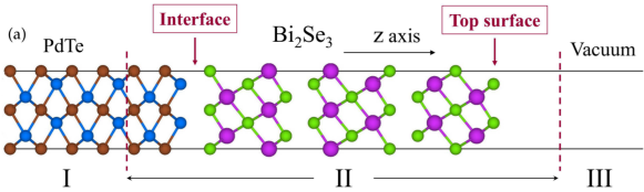
As required in the SKKR formalism, the SC-TI heterostructures are divided into three regions I-III (Fig. 1(a)). Region I and III are semi-infinite PdTe and vacuum layers, respectively. Region II consists of Pd-Te-Pd-Te atomic layers overlaid with Bi2Se3 layers (1-6 QLs) and 4-6 vacuum layers on top. The heterostructures have two-dimensional translational symmetry with the lattice constant of Bi2Se3, 4.143 Å. Our choice of the in-plane lattice constant is made to avoid an effect of strain on the topological surface states Young et al. (2011); Yang et al. (2018). The out-of-plane lattice constant for PdTe is slightly expanded to conserve the volume of PdTe. Otherwise, experimental lattice constants are used. We consider the band structure only along the direction, axis, in this work.
III Results and Discussion
In multiple scattering theory the band structure is obtained from site-dependent Bloch spectral functions (BSF) , where denotes the -th atomic site and is the -th band energy at in-plane momentum . We calculate the BSF for the -th site (located at ) from its retarded Green’s function :
| (1) |
Density of states (DOS) within the SKKR method is obtained from an integral of the BSF over , i.e., . A detailed description of solving the DBdG equations within the fully relativistic SKKR method can be found in Refs.Csire et al., 2015, 2018. A brief method description with parameter values for our simulations is shown in the Supplemental Material (SM).
III.1 Electronic structure of normal state
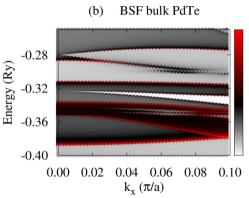
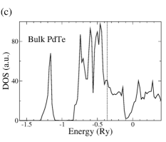
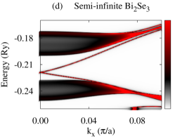
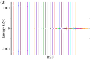
First of all, we present calculated electronic structures of PdTe and Bi2Se3 in the normal state, separately. Figure 1(b) and (c) show BSF contours and DOS of bulk PdTe, respectively. The calculated BSF shows metallic nature. There is a wide range of high electron density below the Fermi level (0.36 Ry) with a sharp DOS peak around 1.20 Ry which arises from Te and orbitals. Figure 1(d) shows BSF contours of a semi-infinite Bi2Se3 system. We find Dirac surface states within a bulk band gap of about 0.03 Ry as well as continuous conduction and valence band regions. For Bi2Se3 slabs, all bands are doubly degenerate due to time-reversal and inversion symmetries, and several QWS appear in the conduction and valence band regions. For a -QL slab, () QWS appear in the conduction (valence) band region Park et al. (2013), as shown in Fig. S1(b),(d) in the SM. For Bi2Se3 slabs thinner than 5-6 QLs, the top and bottom surface states hybridize, opening an energy gap in the Dirac surface states Park et al. (2013); Zhang et al. (2010). This gap is referred to as a surface-hybridization gap. The SKKR-calculated band structures of PdTe and Bi2Se3 agree with those using VASP code Kresse and Furthmuller (1996a, b) (Fig. S1 in the SM).
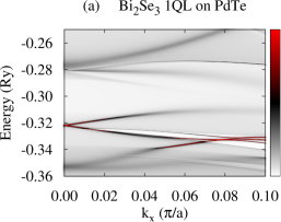
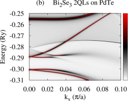
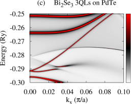
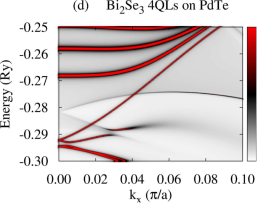
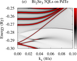
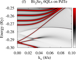
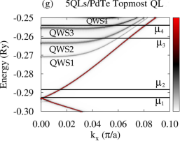
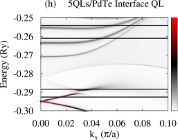
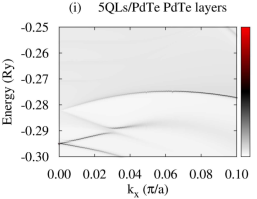
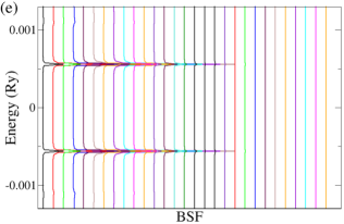
Using the above converged potentials of PdTe and Bi2Se3, we perform fully relativistic SKKR calculations on the Bi2Se3-PdTe heterostructure in the normal state. Figure 2(a)-(f) show calculated normal-state BSF of the heterostructure with the TI film thickness varying from 1 to 6 QLs, where all layers are summed. The gray continuous spectrum in the BSF is similar to that of PdTe. Compare Fig. 2(a)-(f) with Fig. 1(b) or 2(i). We find that a shift of the Madelung potential lowers the TI Dirac point around Ry and that the top-surface and interface Dirac states are shifted from each other with strong modification of the dispersion of the interface Dirac states. The slope of the dispersion near the Dirac point is substantially reduced and the states lose the interface-state character somewhat away from . See Fig. 2(g) and (h). The top-surface (interface) Dirac states are identified as states with a large BSF weight onto the topmost (interface) QL. Strong hybridization of the interface states with the substrate causes the strong modification of their dispersion. Similar effects have been reported in various heterostructures involving Bi2Se3 Govaerts et al. (2014); Hsu et al. (2017). For thin films ( 5 QLs) we also observe an energy gap in the vicinity of the two Dirac points which decreases with increasing the TI overlayer thickness. This gap is induced by the hybridization between the interface and top-surface Dirac states. The shape and number of TI QWS, however, remain unchanged with the substrate, but they are quite broadened compared to the Dirac states, as shown in Fig. 2(b)-(f). This broadening may be caused by scattering of electrons from the substrate. Calculated BSF with finer resolution suggests that each broad QWS peak in Fig. 2 consists of two bands or states. For the 5-QL overlayer on PdTe [Fig. 2(g)], chemical potential Ry crosses three QWS (labeled as QWS1, QWS2, QWS3) and the top-surface Dirac state, while chemical potential Ry crosses only the top-surface and interface Dirac states. For thinner TI overlayers, chemical potential crosses fewer number of QWS compared to the 5-QL overlayer. See Fig. S2 for the characteristics of the QWS.
III.2 Electronic structure of superconducting state
III.2.1 Induced spectral gap with
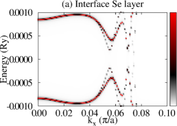
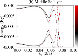
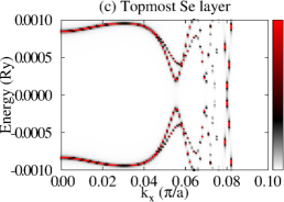
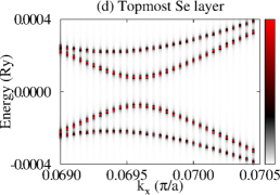
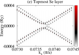
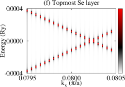
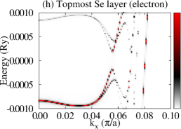
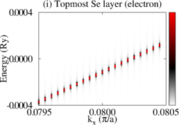
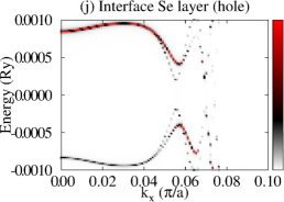
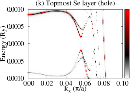
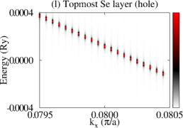
Let us now consider that PdTe is in the SC state with a bulk SC gap of 0.001 Ry and that the TI pairing potential is zero. We then calculate BSF of the heterostructures at a fixed chemical potential. See the SM for the detailed procedure. Figure 3 shows BSF contours of the 5-QL TI overlayer on SC PdTe as a function of energy and at chemical potential Ry. Within the bulk SC gap, we find a highly momentum-dependent proximity-induced gap feature, . In particular, we focus on seven induced gap sizes listed in Table 1. Two large gaps and are clearly seen in Fig. 3(a)-(c). Gap sizes , , , , and are zoomed in in Fig. 3(d)-(f). Except for , all six gap sizes are observed in the BSF of all TI layers. For example, see Fig. 4(c) in the case of . Thus, these gap sizes do not depend on for a fixed TI-overlayer thickness. The induced gap size is larger with smaller . The dispersion near the six gap sizes arises from both electron and hole contributions. See Figs. 3(g),(h),(j),(k), S3, and S4. In the case of , however, the dispersion appears only for the topmost QL and it exhibits a positive (negative) slope only from the electron (hole) contribution. See Fig. 3(i) and (l).
| (Ry) | 0 | ||||||
|---|---|---|---|---|---|---|---|
| () | 0.05550 | 0.05700 | 0.06930 | 0.06960 | 0.07370 | 0.07380 | 0.08023 |
| origin | QWS3 | QWS3 | QWS2 | QWS2 | QWS1 | QWS1 | SS |
The dispersion near the first six induced gaps suggests that Cooper pairs of PdTe tunnel into the TI region, giving rise to the proximity-induced gaps and Andreev bound states. The momentum-dependence and gap sizes can be strongly modified with the interface type and the band structure of non-SC. By comparing the SC-state BSF to the normal-state BSF, we identify that and originate from Cooper-pair tunneling into QWS3 and that and from QWS2. Similarly, and arise from Cooper-pair tunneling into QWS1, and from the top-surface Dirac state. See also Fig. S5. To elucidate the origin of the two different gap sizes from each QWS, we plot normalized SC-state and normal-state BSF at fixed energies and points near the gap size . As shown in Fig. 4(a), the two SC-state BSF qualitatively differ from each other, while the two normal-state BSF are indistinguishable. The state with a larger spectral weight near the interface gives rise to a larger induced gap. Figure 4(c) also clearly shows the two induced gaps at . This two-gap feature is consistent with that of the normal-state BSF (Fig. S6). The induced gap size overall increases as Cooper pairs tunnel into higher-energy QWS because of stronger coupling with the substrate. See Fig. 4(b) and Table 1. The dispersion near (Fig. 3(i) and (l)) is quite distinct from that near the other gaps. Cooper pairs do not seem to efficiently tunnel into the top-surface Dirac state which is strongly localized at the top surface, giving rise to zero induced gap.
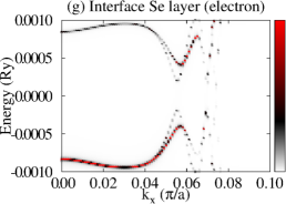
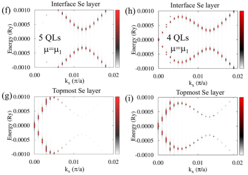
We now investigate the effect of chemical potential on the proximity-induced gap at the 5-QL overlayer by considering , , and , as indicated in Fig. 2(g). For five distinct gap sizes are found. Similarly to the case of , the smallest gap is zero from the top-surface Dirac state, while the rest four gaps are as significant as those for . The dispersion near the four gaps has characteristics of Andreev states. As chemical potential decreases, the number of gaps decreases, whereas the gap size associated with a given QWS type (such as QWS1, QWS2) increases. See Fig. S7. For and , only two gap sizes are observed, and Andreev states exist only near the larger gap. Figure 4(d) and (e) show layer-resolved BSF with , and Fig. 4(f) and (g) show BSF of the interface and topmost layers with . The two gaps appear only closer to the interface QL or the topmost QL. The highly suppressed slope of the dispersion does not allow Cooper pairs to tunnel into the interface TI state until chemical potential reaches near the Dirac points. For and , only top-surface and interface TI states are involved. The induced gap from the interface TI state is largest among the gaps found.
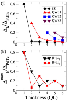
To examine the effect of TI film thickness, we plot the smaller induced gap from each TI-state type (i.e., QWS1, QWS2, QWS3, interface or top-surface) vs thickness at [Fig. 4(j)]. We find that the induced gap from higher-energy QWS decays much slowly than that from lower-energy QWS, and that the gap from the top-surface Dirac state becomes zero for thickness greater than 3 QLs. Figure 4(k) shows the ”maximum” gap from the gap sizes shown in Fig. 4(j) as a function of overlayer thickness, at and . Interestingly, the ”maximum” gap oscillates with thickness. For overlayers thinner than 5 QLs, the surface-hybridization effect is also seen in the induced gap. The gap size from the top-surface Dirac state becomes noticeable, and the induced gap sizes do not depend on . Compare Fig. 4(h) and (i) with Fig. 4(f) and (g) for . Tables in the SM list all induced gap sizes.
III.2.2 Induced spectral gap with
We study an effect of the TI pairing potential by keeping same as before and considering that . Although electron-phonon coupling of the TI cannot induce superconductivity itself, it can create a finite pairing potential induced by the superconductor Fu and Kane (2008). Figure 5(a) shows effective pairing potential calculated self-consistently for the 5-QL overlayer on PdTe using semi-phenomenological parameters within the SKKR method. See the SM for the detailed procedure. As shown in the inset, the pairing potential decays very slowly in the TI region. With this calculated pairing potential, we obtain BSF for the 5-QL overlayer on SC PdTe at . As listed in Table 2, the induced gap from the top-surface Dirac state becomes noticeable with Andreev-state characteristics (Fig. 5(b)-(d)), whereas the gap from high-energy QWS does not change much compared to the case of zero TI pairing potential. We expect that topological edge states within the smallest induced gap can trap Majorana zero-modes with broken time-reversal symmetry Fu and Kane (2008); Alicea (2012) and that pairing type of the proximity-induced superconductivity may be identified from gap anisotropy Alicea (2012) and/or unique spin-orbital textures of the Andreev states Fukaya et al. (2019).
| [Fig. 5(a)] | ||
|---|---|---|
| QWS3 | 0.220 | 0.200 |
| QWS2 | 0.110 | 0.080 |
| QWS1 | 0.056 | 0.016 |
| SS | 0.030 | 0 |
III.3 Comparison with experiment
Let us make brief qualitative comparison of our results with experimental and model-Hamiltonian studies, considering that our SC substrate differs from those used in experiments. Refs. Xu et al., 2014a; Flototto et al., 2018 showed momentum-resolved proximity-induced gaps using ARPES. In Ref. Xu et al., 2014a the proximity-induced gap from the bulk TI state significantly differs from the gap from the TI surface state, while in Ref. Flototto et al., 2018 that is not the case. Our results are consistent with the former experimental data whether is set to zero or not. The discrepancy may originate from the experimental difficulty in identifying the peak center of the spectral function corresponding to the bulk and surface states. We find that an accurate estimate of the induced gap from the TI surface state requires a high precision in momentum such as 10-5 . With a precision of 0.001 , the induced gap can be overestimated by two orders of magnitude. However, the induced gap from bulk states is insensitive to the precision of momentum. Compared to STM experimental data Wang et al. (2012); Xu et al. (2014b), we obtain underestimated induced gaps even for . Model-Hamiltonian studies predicted the zero gap from the top-surface TI state for thick TI overlayers Stanescu et al. (2010); Chiu et al. (2016), which is consistent with our result. However, the rich features of the induced gaps that we find were not obtained from the model-Hamiltonian approaches.
IV Conclusion
In summary, we simulated Bi2Se3 films of 1-6 nm overlaid on SC PdTe by solving the DBdG equations with two pairing potential profiles within the SKKR method, finding that the strong -dependence of the proximity-induced gap arises from the unique TI band structure and its modifications under the SC substrate. The size of the induced gap strongly varies with characteristics of TI states which are partially occupied at the Fermi level. Cooper pairs tunnel into higher-energy QWS more efficiently and the induced gap from higher-energy QWS decreases more slowly with increasing TI film thickness. For thick TI films, the induced gap from the top-surface Dirac state becomes zero with zero TI pairing potential, whereas the gap can be substantial for finite TI pairing potential. For a given thick TI film, the induced gap from the interface Dirac state appears only near the interface QL, although the induced gap size from each QWS does not depend on . Our findings demonstrate an importance of consideration of the realistic TI band structure for studies of the superconducting proximity effect, and they can be used for future larger-scale simulations and experimental studies of topological edge states or nanowires on SC substrates in pursuit of Majorana zero-modes.
Acknowledgements.
We are grateful to Peter Rakyta for setting up initial Bi2Se3 structures. The computational support was provided by San Diego Supercomputer Center under DMR060009N and Virginia Tech Advanced Research Computing. BU was supported by the Hungarian National Research, Development and Innovation Office under Contract No. K131938 and BME Nanotechnology FIKP grants. GC acknowledges support from the European Unions Horizon 2020 research and innovation programme under the Marie Sklodowska-Curie grant agreement No. 754510.References
- Kitaev (2001) A. Y. Kitaev, Phys.-Usp. 44, 131 (2001).
- Fu and Kane (2008) L. Fu and C. L. Kane, Phys. Rev. Lett. 100, 096407 (2008).
- Alicea (2012) J. Alicea, Rep. Prog. Phys. 75, 076501 (2012).
- Yang et al. (2012) F. Yang, F. Qu, J. Shen, Y. Ding, J. Chen, Z. Ji, G. Liu, J. Fan, C. Yang, L. Fu, and L. Lu, Phys. Rev. B 86, 134504 (2012).
- Wang et al. (2012) M.-X. Wang, C. Liu, J.-P. Xu, F. Yang, L. Miao, M.-Y. Yao, C. L. Gao, C. Shen, X. Ma, X. Chen, Z.-A. Xu, Y. Liu, S.-C. Zhang, D. Qian, J.-F. Jia, and Q.-K. Xue, Science 336, 52 (2012).
- Xu et al. (2014a) S.-Y. Xu, N. Alidoust, I. Belopolski, A. Richardella, C. Liu, M. Neupane, G. Bian, S.-H. Huang, R. Sankar, C. Fang, B. Dellabetta, W. Dai, Q. Li, M. J. Gilbert, F. Chou, N. Samarth, and M. Z. Hasan, Nat. Phys. 10, 943 (2014a).
- Xu et al. (2014b) J.-P. Xu, C. Liu, M.-X. Wang, J. Ge, Z.-L. Liu, X. Yang, Y. Chen, Y. Liu, Z.-A. Xu, C.-L. Gao, D. Qian, F.-C. Zhang, and J.-F. Jia, Phys. Rev. Lett. 112, 217001 (2014b).
- He et al. (2014) Q. L. He, H. Liu, M. He, Y. H. Lai, H. He, G. Wang, K. T. Law, R. Lortz, J. Wang, and I. K. Sou, Nat. Commun. 5, 4247 (2014).
- Xu et al. (2015) J.-P. Xu, M.-X. Wang, Z. L. Liu, J.-F. Ge, X. Yang, C. Liu, Z. A. Xu, D. Guan, C. L. Gao, D. Qian, Y. Liu, Q.-H. Wang, F.-C. Zhang, Q.-K. Xue, and J.-F. Jia, Phys. Rev. Lett. 114, 017001 (2015).
- Flototto et al. (2018) D. Flototto, Y. Ota, Y. Bai, C. Zhang, K. Okazaki, A. Tsuzuki, T. Hashimoto, J. N. Eckstein, S. Shin, and T.-C. Chiang, Sci. Adv. 4, eaar7214 (2018).
- Sun et al. (2017) H.-H. Sun, M.-X. Wang, F. Zhu, G.-Y. Wang, H.-Y. Ma, Z.-A. Xu, Q. Liao, Y. Lu, C.-L. Gao, Y.-Y. Li, C. Liu, D. Qian, D. Guan, and J.-F. Jia, Nano Lett. 17, 3035 (2017).
- Mourik et al. (2012) V. Mourik, K. Zuo, S. M. Frolov, S. R. Plissard, E. P. A. M. Bakkers, and L. P. Kouwenhoven, Science 336, 1003 (2012).
- Gül et al. (2017) O. Gül, H. Zhang, F. K. de Vries, J. van Veen, K. Zuo, V. Mourik, S. Conesa-Boj, M. P. Nowak, D. J. van Woerkom, M. Quintero-PÃrez, M. C. Cassidy, A. Geresdi, S. Koelling, D. Car, S. R. Plissard, E. P. A. M. Bakkers, and L. P. Kouwenhoven, Nano Lett. 17, 2690 (2017).
- Zhang et al. (2018) H. Zhang, C.-X. Liu, S. Gazibegovic, D. Xu, J. A. Logan, G. Wang, N. van Loo, J. D. S. Bommer, M. W. A. de Moor, D. Car, R. L. M. Op het Veld, P. J. van Veldhoven, S. Koelling, M. A. Verheijen, M. Pendharkar, D. J. Pennachio, B. Shojaei, J. S. Lee, C. J. PalmstrÃm, E. P. A. M. Bakkers, S. D. Sarma, and L. P. Kouwenhoven, Nature 556, 74 (2018).
- Nadj-Perge et al. (2014) S. Nadj-Perge, I. K. Drozdov, J. Li, H. Chen, S. Jeon, J. Seo, A. H. MacDonald, B. A. Bernevig, and A. Yazdani, Science 346, 602 (2014).
- Feldman et al. (2017) B. E. Feldman, M. T. Randeria, J. Li, S. Jeon, Y. Xie, Z. Wang, I. K. Drozdov, B. Andrei Bernevig, and A. Yazdani, Nat. Phys. 13, 286 (2017).
- Ruby et al. (2017) M. Ruby, B. W. Heinrich, Y. Peng, F. von Oppen, and K. J. Franke, Nano Lett. 17, 4473 (2017).
- Palacio-Morales et al. (2019) A. Palacio-Morales, E. Mascot, S. Cocklin, H. Kim, S. Rachel, D. K. Morr, and R. Wiesendanger, Sci. Adv. 5, eaav6600 (2019).
- Kitaev (2003) A. Kitaev, Ann. Phys. 303, 2 (2003).
- Stanescu et al. (2010) T. D. Stanescu, J. D. Sau, R. M. Lutchyn, and S. Das Sarma, Phys. Rev. B 81, 241310 (2010).
- Lababidi and Zhao (2011) M. Lababidi and E. Zhao, Phys. Rev. B 83, 184511 (2011).
- Black-Schaffer and Balatsky (2013) A. M. Black-Schaffer and A. V. Balatsky, Phys. Rev. B 87, 220506 (2013).
- Chiu et al. (2016) C.-K. Chiu, W. S. Cole, and S. Das Sarma, Phys. Rev. B 94, 125304 (2016).
- Fu et al. (2007) L. Fu, C. L. Kane, and E. J. Mele, Phys. Rev. Lett. 98, 106803 (2007).
- (25) H. Zhang, C.-X. Liu, X.-L. Qi, X. Dai, Z. Fang, and S.-C. Zhang, .
- Capelle and Gross (1999) K. Capelle and E. K. U. Gross, Phys. Rev. B 59, 7140 (1999).
- Csire et al. (2015) G. Csire, B. Ujfalussy, J. Cserti, and B. Gyorffy, Phys. Rev. B 91, 165142 (2015).
- Csire et al. (2018) G. Csire, A. Deak, B. Nyari, H. Ebert, J. F. Annett, and B. Ujfalussy, Phys. Rev. B 97, 024514 (2018).
- Nakajima (1963) S. Nakajima, J. Phys. Chem. Solids 24, 479 (1963).
- Karki et al. (2012) A. B. Karki, D. A. Browne, S. Stadler, J. Li, and R. Jin, J. Phys.: Condens. Matter 24, 055701 (2012).
- Zhu et al. (2012) X. Zhu, L. Santos, C. Howard, R. Sankar, F. C. Chou, C. Chamon, and M. El-Batanouny, Phys. Rev. Lett. 108, 185501 (2012).
- Young et al. (2011) S. M. Young, S. Chowdhury, E. J. Walter, E. J. Mele, C. L. Kane, and A. M. Rappe, Phys. Rev. B 84, 085106 (2011).
- Yang et al. (2018) W. J. Yang, C. W. Lee, D. S. Kim, H. S. Kim, J. H. Kim, H. Y. Choi, Y. J. Choi, J. H. Kim, K. Park, and M.-H. Cho, J. Phys. Chem. C 122, 23739 (2018).
- Park et al. (2013) K. Park, C. D. Beule, and B. Partoens, 15, 113031 (2013).
- Zhang et al. (2010) Y. Zhang, K. He, C.-Z. Chang, C.-L. Song, L.-L. Wang, X. Chen, J.-F. Jia, Z. Fang, X. Dai, W.-Y. Shan, S.-Q. Shen, Q. Niu, X.-L. Qi, S.-C. Zhang, X.-C. Ma, and Q.-K. Xue, Nat. Phys. 6, 584 (2010).
- Kresse and Furthmuller (1996a) G. Kresse and J. Furthmuller, Phys. Rev. B 54, 11169 (1996a).
- Kresse and Furthmuller (1996b) G. Kresse and J. Furthmuller, Comput. Mater. Sci. 6, 15 (1996b).
- Govaerts et al. (2014) K. Govaerts, K. Park, C. De Beule, B. Partoens, and D. Lamoen, Phys. Rev. B 90, 155124 (2014).
- Hsu et al. (2017) Y.-T. Hsu, K. Park, and E.-A. Kim, Phys. Rev. B 96, 235433 (2017).
- Fukaya et al. (2019) Y. Fukaya, S. Tamura, K. Yada, Y. Tanaka, P. Gentile, and M. Cuoco, Phys. Rev. B 100, 104524 (2019).