Random 2D nanowire networks: Finite-size effect and the effect of busbar/nanowire contact resistance on their electrical conductivity
Abstract
We have studied the resistance of two-dimensional random percolating networks of zero-width metallic nanowires (rings or sticks). We toke into account the nanowire resistance per unit length, the junction (nanowire/nanowire contact) resistance, and the busbar/nanowire contact resistance. Using a mean-field approximation (MFA), we derived the total resistance of the nanoring-based networks as a function of their geometrical and physical parameters. We have proposed a way of accounting for the contribution of the busbar/nanowire contact resistance toward the network resistance. The MFA predictions have been confirmed by our Monte Carlo (MC) numerical simulations. Our study evidenced that the busbar/nanowire contact resistance has a significant effect on the electrical conductivity when the junction resistance dominates over wire resistance.
I Introduction
In recent years, the study of random two-dimensional (2D) networks of conductive nanowires has become a hot topic of research. Due to the excellent electrical and optical performances of such systems, numerous applications are possible, while their low cost and ease of manufacturing promise very attractive prospects.[1]
A comprehensive review of the different approaches used to describe the behavior of the electrical conductivity of random 2D nanowire networks can be found in Ref. 2. This review should be extended by some recently published works devoted to nanostick- and nanowire-based random 2D networks.[3, 4, 5, 6, 7, 8, 9] Benda, Cancès, and Lebental [2] proposed a closed-form approximation of the functional dependence of the effective resistance () of 2D random networks of zero-width stick nanowires on their physical parameters
| (1) |
where is the wire resistance, is the junction resistance (wire-to-wire contact resistance), and is the busbar/wire contact resistance, while , , and are the geometrical coefficients. Similar relations have been proposed by other authors.[10, 11, 12, 3] However, in those works, only the wire resistance and the junction resistance were taken into account, while the busbar/wire contact resistance was ignored. A consideration of the busbar/wire contact resistance as an independent and significant parameter is an important novelty of Ref. 2. This dependence has been derived using a dimensional analysis (-theorem). However, the coefficients , , and have been obtained using a fit of MC simulations rather than from an analytical consideration. These coefficients depend on both the geometry (the aspect ratio of electrode separation over stick length) and the number of wires with respect to the number of wires at the percolation threshold. However, the percolation threshold was not explicitly used in the derivation of Eq. (1). By contrast, the percolation threshold and the two critical exponents were taken into account in Ref. 10, viz., the sheet resistance of dense networks of randomly placed zero-width sticks is
| (2) |
where is the linear system size, is the length of the stick, is the number density of the conductive sticks (number of sticks per unit area), is the percolation threshold, , , and are adjustable parameters, is the correlation-length exponent, and is the conductivity exponent.[10] Since the critical exponents as well the number of particles at the percolation threshold are dimensionless, these quantities can readily be incorporated into dimensional analyse.
The resistance of the contacts of the conductive wires with the busbars was taken into account in computations by Forró et al. [13] However, their conductivity estimates using an MFA ignored this resistance. To reconcile the MFA predictions and computations, the authors introduced a correction factor (a so-called “effective wire length”). In our own recent computations, the busbar/wire resistance was 0, so the consistency of the computations and the MFA predictions was provided without any correction factor being required.[9]
In the case of nanoring-based films, when the junction resistance dominates over the wire resistance while the busbar/nanowire contact resistance and the junction resistance are of the same order of magnitude, the MFA significantly overestimates the electrical conductivity when compared to the computations.[7] Thus, the contribution of the busbar/wire resistance to the sheet resistance seems to be important.
The increased effective length associated with microstructured electrodes results in modifications of the electrical device behavior within the same Ag nanowire network.[14] Reduction of 10–40% was observed in the sheet resistance, with the strongest reductions for devices with two serrated electrodes. The nanowires had mean diameters of nm and lengths of m. Active network areas were and m. Hence, the values of the ratio were from 6.67 to 26.67. For the flat electrode devices, the authors reported . Note that the sizes of nanowire-based films can be very different, viz., mm,[15] mm,[16] m.[17]
Reported data evidenced that the ratio of Ag nanowire length to its diameter ranges from 100 to 1000 of the order of magnitude (Table 1), i.e., a slender-rod approximation seems to be valid. Four-probe measurements on almost 40 individual nanowires with diameters ranging from 50 to 90 nm gave an average resistivity of nm.[18] Gomes da Rocha et al. [17] reported similar value of the average Ag nanowire resistivity, viz., nm obtain using 15 Ag nanowires.[17] Using three different methods, the junction resistance for Ag nanowires was determined. The distribution shows a strong peak at , corresponding to the median value of the distribution.[18] Selzer et al. [19] reported that a value of the resistance of a single Ag nanowire is m while the junction resistance is (annealed junctions) and (non-annealed ones). Out estimates (the last column of Table 1) evidenced that, typically, the junction resistance is significantly larger than the wire resistance (up to 2 orders of magnitude), .
| Reference | length , m | diameter , nm | , | |
|---|---|---|---|---|
| ( nm) | ||||
| Lee et al. [20] | ||||
| Nguyen et al. [21] | ||||
| Khanarian et al. [22] | 4,8–36 | 56–153 | 31–360 | |
| He et al. [23] | ||||
| Gomes da Rocha et al. [17] | ||||
| Selzer et al. [19] | ||||
| Bellew et al. [18] | ||||
| Kou et al. [15] | ||||
| Xu et al. [24] | 120 | |||
| Oh et al. [25] | ||||
| Lee et al. [26] | 16–22 |
Silver nanorings with the uniform ring diameter of m can also be synthesized.[27, 28] Depending on the nanoring concentration, the sheet resistance of nanoring-based films of size cm varies from 20 to 350 .[28] In these samples, the ratio of the linear system size to the nanoring diameter is approximately 3000.
The goal of our study was to evaluate the contribution of the busbar/nanowire contact resistance in the total resistance of 2D systems of randomly placed conductive wires. For this purpose, we derived a closed-form expression for the effective electrical resistance as a function of the main physical parameters including the busbar/nanowire contact resistance. An MC simulation has been performed to test this expression.
The rest of the paper is constructed as follows. Section II.1 is devoted to our simulation. Since details of the computer simulation have been described previously,[28, 7, 9, 8] we present in Sec. II.1 only a brief sketch using the nanoring-based system as an example. The electrical conductivity of the system of randomly placed conductive rings using a discreet version of the MFA is derived in Sec. II.2. The effect of the busbars on the electrical resistance is analyzed in Sec. II.3. In Section III, we compare our MC simulations and theoretical predictions. Section IV summarizes the main results and discusses some open questions.
II Methods
II.1 Computer simulation
Sampling is very close to the used previously.[28, 7, 8, 9] Identical conductive fillers were randomly placed on a substrate. Their centers were independent and identically distributed within a square domain of size . To reduce the finite-size effect, periodic boundary conditions (PBCs) were applied along both mutually perpendicular directions. Since the electrical conductivity is our primary interest, the number density was required to be above the percolation threshold, . When the desired number density of the fillers was reached, the PBCs were removed, allowing us to consider the model as an insulating film of size covered by conductive fillers. Two opposite borders of the domain were considered as superconductive busbars. A potential difference, , was applied to these busbars. The electrical resistance per unit length of each filler is . The electrical resistance of each contact (junction) between any two fillers is . The electrical resistance of each contact (junction) between a filler and a busbar is . Junctions are assumed to be ohmic. The system under consideration can be treated as a random resistor network (RRN). Such a network is an irregular network with different branch resistances. Applying Ohm’s law to each branch and Kirchhoff’s point rule to each junction, a system of linear equations (SLEs) can be written. Although this SLE is huge, its matrix is sparse. We used the EIGEN library[29] to solve it numerically.
Two particular kinds of fillers were considered, viz, rings with a given radius (, ) and equiprobable orientated zero-width sticks with a given length ().
Generally, we used domains of the fixed size . An additional study of the finite-size effect was performed. To efficiently determine the percolation threshold (occurrence of a percolation cluster that spans the system in a given direction), the union-find algorithm [30, 31] was used. In our simulations, for rings, while for sticks.
Computations for systems of randomly placed zero-width conductive sticks were carried out similarly. Depending on which effect was of interest, in the figures we used either the resistance or the electrical conductivity as alternatives. The results of the computations were averaged over 100 independent runs. The error bars in the figures correspond to the standard deviation of the mean. When not shown explicitly, they are of the order of the marker size.
II.2 Mean-field approach for randomly placed conductive rings
When the number density of the conductive rings is large enough, the variation of the electrical potential along the film is close to linear.[28] The basic idea behind the MFA is as follows. Only one conductive ring in the mean-field produced by all the other rings can be considered instead of a consideration of the entire network. Let there be a conductive ring of radius placed in an external electrostatic field (Fig. 1). The potential of the external field depends on the coordinate, . The conductive ring is assumed to be covered with an ideal insulator. Each intersection of this ring with other rings (junctions) in the original system is considered in the MFA as an insulation imperfection that can lead to some leakage current. Thus, each junction is assumed to be possessed of an electrical resistance .
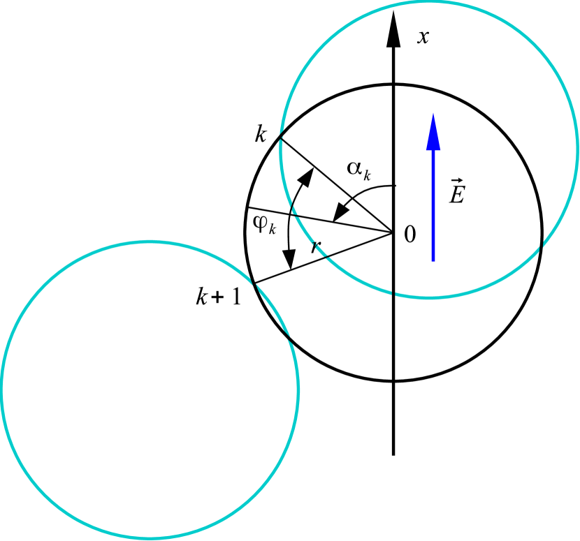
Consider the arc of the ring between the -th and the -th contacts (Fig. 1). Let the central angle of this arc be , while the angle between the direction of the external electrostatic field and the direction from the ring center to the center of the arc be equal to . The resistance of the arc between these two contacts is equal to .
According to Ohm’s law, the potential drop along the arc is
| (3) |
where and are the potentials of the contacts and , respectively, while is the electrical current in the arc between these contacts. According to Kirchhoff’s rule, for the -th contact
| (4) |
where is the potential of the external field at the point where the -th contact is located. Hence, the potential of the -th contact, , can be written as
| (5) |
The potential of the -th contact, , can be written similarly. Substitution of the potential drop between these two contacts into Eq. (3) leads to
| (6) |
Taking the center of the ring as the zero potential of the external field, we get the dependence of the potential on the angular coordinate
| (7) |
where is the angle between the direction of the electrostatic field and the radius vector that connects the center of the ring with the given point. Accordingly, the potential of the external field at the -th contact is
| (8) |
while the potential of the external field at the -th contact is
| (9) |
Then,
| (10) |
Hence, Eq. (6) can be rewritten as
| (11) |
To solve this recurrence relation, some additional assumptions are required.
Let . Then,
| (12) |
According to Ref. 32, the probability density function (PDF) for the arc’s central angle is
| (13) |
when . Multiply equation (12) by the PDF (13) and then integrate over all angles
| (14) |
Thus, the electrical current in the -th arc is
| (15) |
The average current at the point of the ring that has the angular coordinate , is equal to
| (16) |
or, in Cartesian coordinates,
| (17) |
The total electrical current that is carried by all the rings intersecting a given equipotential line, is
| (18) |
According to the continuum (vector) form of Ohm’s law . Hence, the formula for the electrical conductance is
| (19) |
This formula coincides with that which was obtained within the framework of the continuous approximation.[7]
Now, let us assume that the contacts are evenly distributed over the ring. Hence, the angle between any two nearest contacts is , while and . Thus, Eq. (11) transforms in
| (20) |
We will look for a solution to the recurrence relation (20) in the form . Substitution of this guest solution into Eq. (20) leads to
| (21) |
since and . Thus, the electrical current in the -th arc is
| (22) |
The total electrical current that is carried by all the rings intersecting a given equipotential line, is
| (23) |
The electrical conductance is
| (24) |
while the electrical resistance is
| (25) |
Formula (24) coincides with the formula obtained using a continuous approach.[7]
II.3 Effect of busbars
We will distinguish between the potential difference applied to the busbars, , and the potential difference, , between the boundaries of the internal region of the system under consideration. Only when the resistance of the contacts of the conductive wires (sticks, rings, etc.) with the busbars is zero, does . Otherwise, the voltage drops at the contacts of the conductive wires with the busbars should be taken into consideration. The average voltage drop at each busbar/wire contact is
| (26) |
where is the number of contacts between the wires and the busbar. Since there are two busbars, . Accounting for the continuum form of Ohm’s law,
| (27) |
Hence, the effective resistance accounting for the busbar/wire contact resistance is
| (28) |
In our particular case, , hence,
| (29) |
Substituting (24) into (29), we get the formula
| (30) |
Both the system size and the busbar/nanowire resistance are presented only in the last term. Hence, the last term describes both a finite-size effect and the effect of the busbar/nanowire resistance on the electrical conductivity. This term is especially significant when [the so-called “junction dominated approach” (JDA)[33] or, alternatively, the “junction resistance dominant assumption” (JRDA)[4]]. Comparison of (1) and (30) clearly evidenced that , , and . In the thermodynamic limit (), the resistance of the system is determined only by the two first terms of formula (30), i.e., it is independent of the resistance of the contacts of the conductors with the busbars.
Thus, for a 2D nanoring-based random system, an analog of Eq. (1) is obtained. In contrast with Ref. 2, the explicit expressions for the geometrical coefficients are presented for the system under consideration.
The above method can easily be transferred to other 2D systems, e.g., random metallic nanowire networks with zero-width rodlike wires (sticks).[9, 8] For a dense system,[9, 8]
| (31) |
where
| (32) |
In this case, the number of contacts between the wires and a busbar is
| (33) |
where is the stick length. Hence,
| (34) |
Using a series expansion of (31), the effective resistance can be split into three terms like (1)
| (35) |
Hence, the finite-size effect and the effect of the busbar/nanowire resistance on the electrical conductivity can be studied independently of other effects. Again, comparison of (1) and (35) evidenced that , , and . In the thermodynamic limit (), the resistance of the system is determined only by the two first terms of formula (35), i.e., it does not depend on the resistance of the contacts of the conductors with the busbars. When the junction resistance dominates over the wire resistance, Eq. (35) is simplified, then
| (36) |
III Results
III.1 Ring-based conductive films
Figure 2 presents the dependencies of the average electrical current, , on the position in the conductive ring, for different values of the number density. Here, 0 corresponds to the ring center. The lines correspond to the MFA prediction (17). Figure 2 evidenced that the MFA prediction is reasonable only for sufficiently dense systems. This is quite expected, since the assumption was used in the derivation.
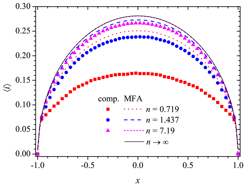
Figure 3 shows the potential distribution in one particular sample with randomly placed conductive rings (, , ). The potential drop along the sample is close to linear. The potential of each junction in the system is plotted here against its position in the sample. However, although the busbar potentials are 0 and 1, the potentials of the contacts closest to the busbars differ markedly from these values.
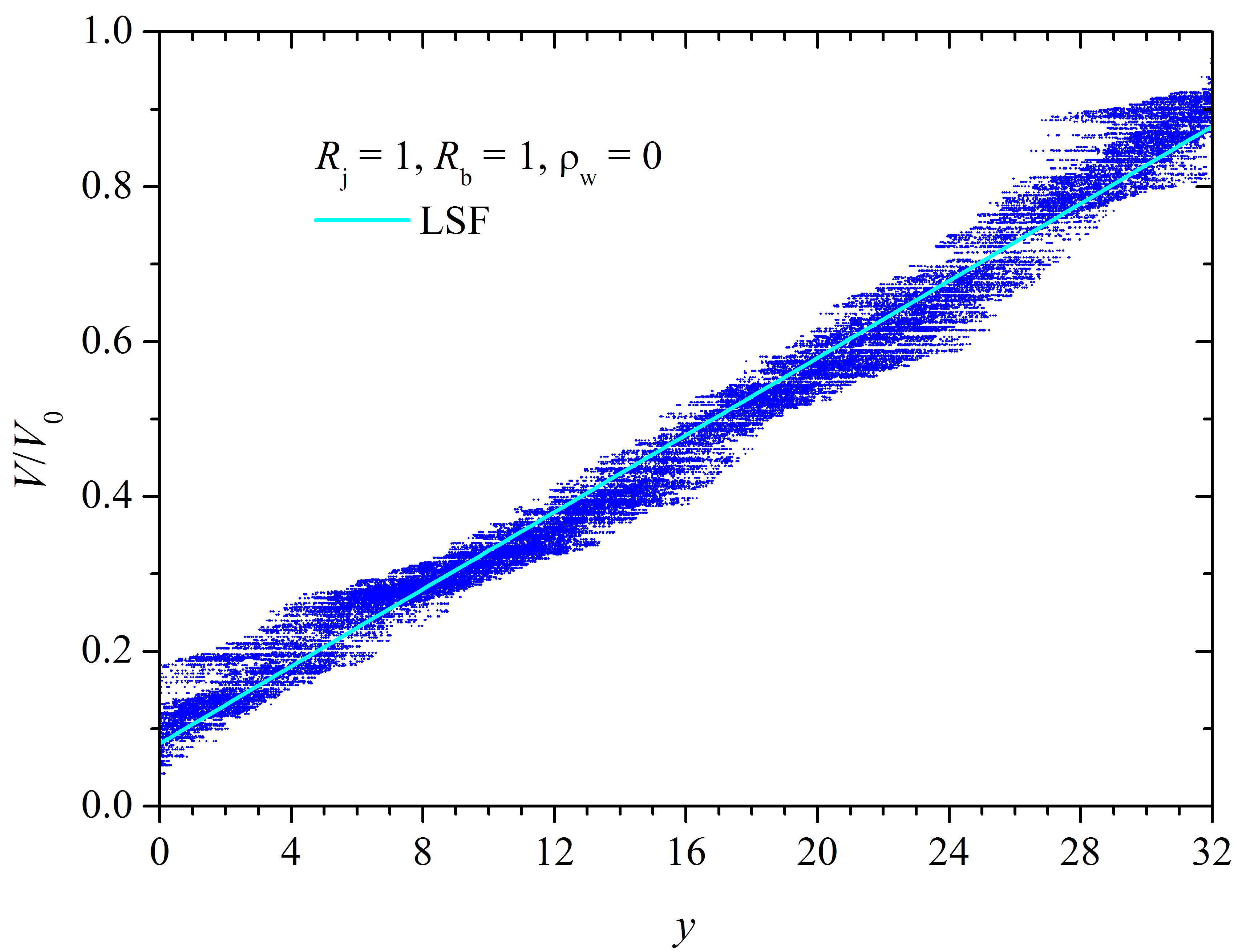
Figure 4 exhibits the electrical conductance against the number density of the conductive rings when the junction resistance dominates over the wire resistance (, ). In this particular case, Eq. (30) leads to the electrical conductance
| (37) |
The markers correspond to the direct computation of the electrical conductance, viz., (squares) and (circles) (see Section II.1 for details). The solid lines correspond to the least squares fit (LSF) using a polynomial of the second degree, while the dashed lines correspond to the MFA. Figure 4 evidenced that accounting for the busbar/nanowire contact resistance is crucial when the junction resistance dominates over the wire resistance. The MFA correctly describes the behavior of the electrical conductivity for .
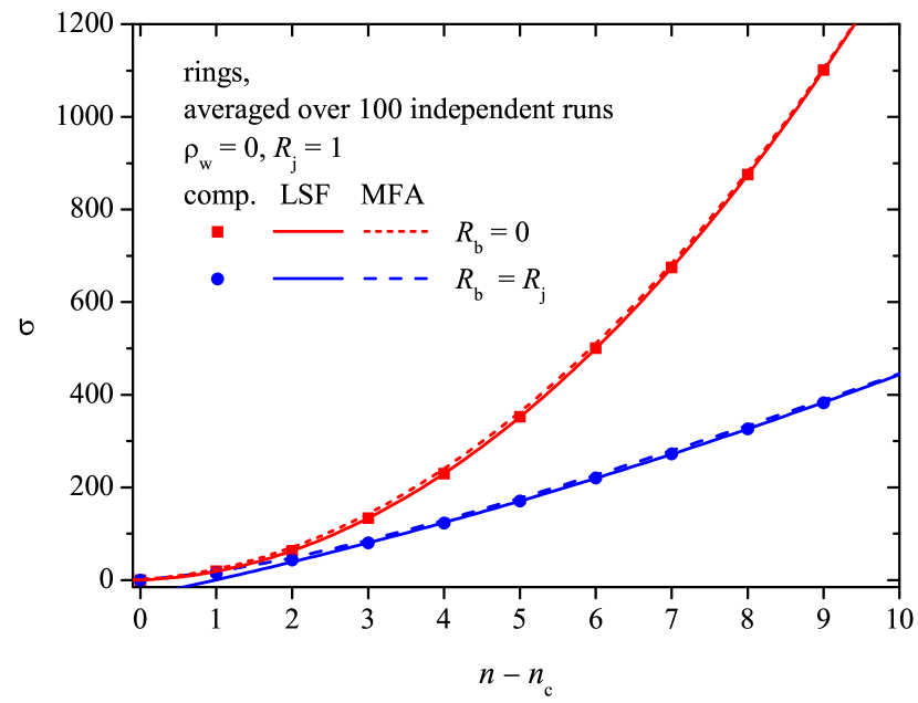
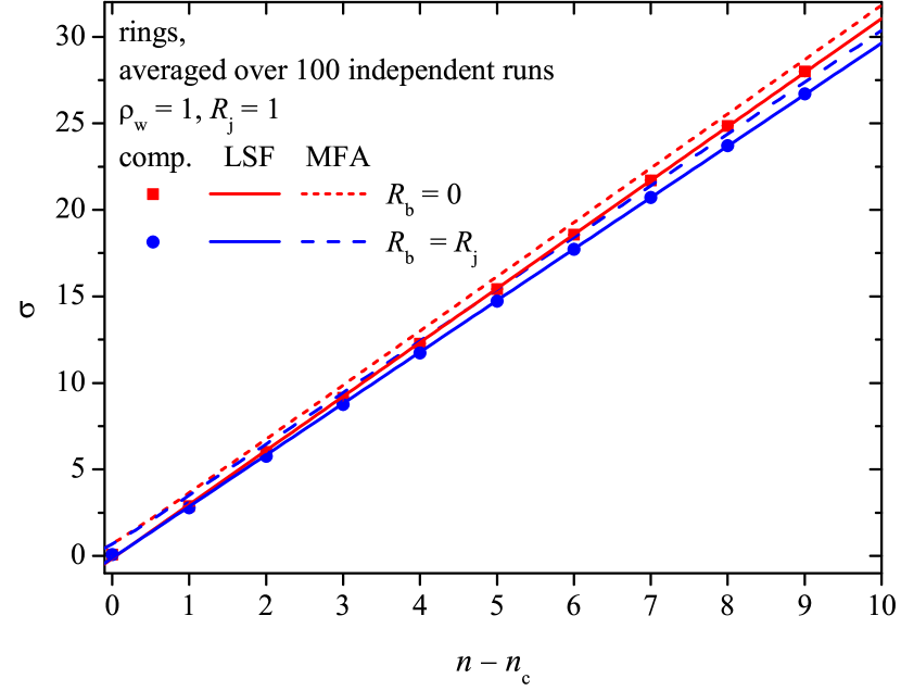
Figure 5 demonstrates the electrical conductance against the number density of the conductive rings when the wire resistance dominates over the junction resistance (, ). In this particular case, Eq. (30) leads to the electrical conductance
| (38) |
The markers correspond to the direct computation of the electrical conductance, viz., (squares) and (circles). The solid lines correspond to the LSF using a linear function. The dashed lines correspond to the MFA. Again, the MFA correctly describes the behavior of the electrical conductance when the wire resistance dominates over the junction resistance. However, the effect of the busbars is much smaller as compared to the previous case.
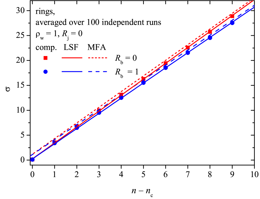
Figure 6 shows the electrical conductance against the number density of the conductive rings when the wire resistance equals the junction resistance (, ). The markers correspond to the direct computation of the electrical conductance, viz., (squares) and (circles). The solid lines correspond to the LSF using a linear function. The dashed lines correspond to the MFA. In this common case, , where is defined by Eq. (30).
To check the contribution of the busbars to the electrical resistance, the dependencies of the resistance on the system size, , as well as on the number density, , have been studied. Formulae (30) and (36) predict a linear dependency of this contribution, both on and on .
Figure 7 demonstrates the electrical resistance against the reciprocal number density for different values of the ratio when . The results of the direct computations (markers) are compared with the predictions of the MFA (lines). The larger the number density, the more accurate the prediction, since the contribution of the ring/ring contacts to the electrical resistance decreases rapidly as .
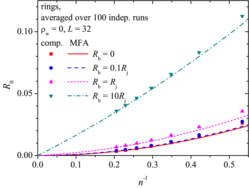
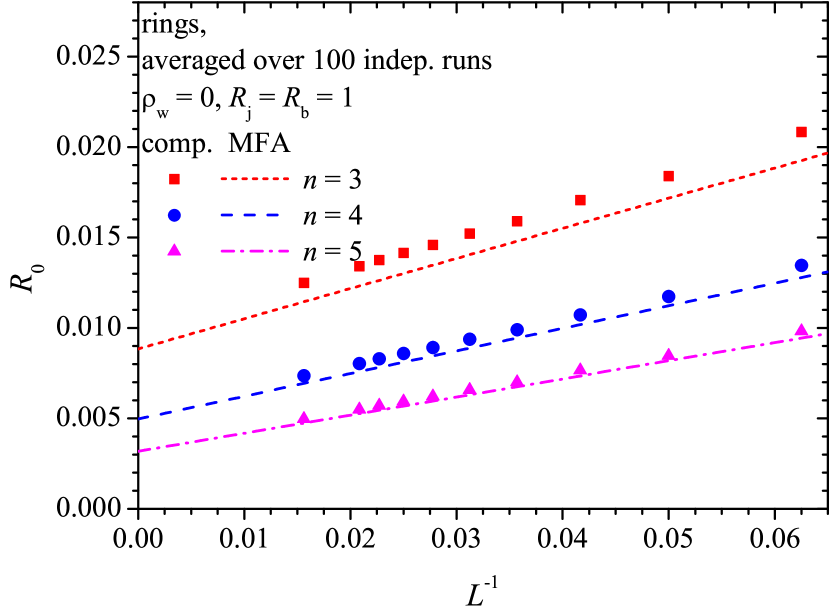
Figure 8 presents the resistance against the reciprocal linear size of the system under consideration for the three different values of the number density when , . The lines correspond to Eq. (30). As the size of the system increases, the contribution of the busbars to the resistance decreases.
III.2 Stick-based conductive films
Figure 9 shows the dependency of the potential jump between the busbar and a conductor on the value of the ratio for systems of randomly placed conductive sticks. Combination of Eqs. (26), (36), and (33) with Ohm’s law leads to
| (39) |
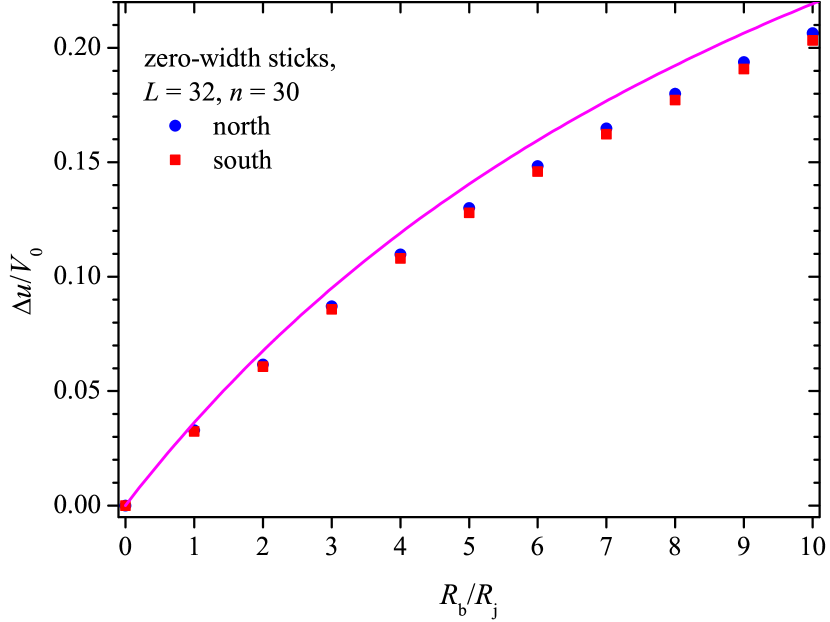
Figure 10 demonstrates the electrical resistance against the reciprocal number density for different values of the ratio when . The results of the direct computations (markers) are compared with the predictions of the MFA (lines). The larger the number density, the more accurate the prediction, since the contribution of the stick/stick contacts to the electrical resistance decreases rapidly as .
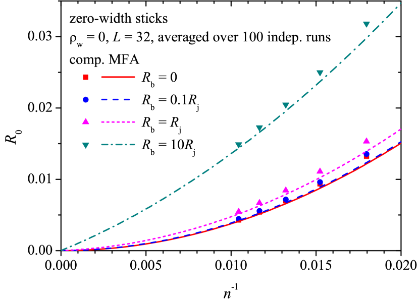
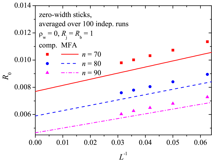
Figure 11 presents the resistance against the reciprocal linear size of the system under consideration for the three different values of the number density when , . The lines correspond to Eq. (36). As the size of the system increases, the contribution of the busbars to the resistance decreases. The results of computer simulations show the same trend as theoretical predictions.
IV Conclusion
We found that the busbar/nanowire contact resistance is crucial when the junction resistance, , dominates over the wire resistance, . Accounting for the busbar/nanowire contact resistance leads to a correct description of the behavior of the electrical conductivity for any ratio within the MFA. Recently, a deviation between computations and the MFA predictions in systems of randomly placed conductive rings when , while has been reported.[7] In the present study, we have shown that this discrepancy is completely eliminated if, when carrying out a theoretical assessment of the electrical conductivity, the busbar/nanowire contact resistance is taken into account. However, in the thermodynamic limit (), the electrical resistance of the system under consideration is independent on the resistance of the contacts of the conductors with the busbars. Comparison of (1) with (30) and (35) evidenced that , , and ( in the case of rings). These exponents of for and are consistent with the exponents proposed for large dense networks, well above the percolation threshold.[10] However, these exponents are noticeably different from those obtained for small systems ().[2]
In the case of nanorod-based 2D systems, the transition from a continuous consideration in the framework of the MFA[9] to a discrete one[8] somewhat improved the estimates of the electrical conductivity. By contrast, in the case of nanoring-based 2D systems, the discrete consideration in the framework of the MFA, carried out in the present study, gave no improvement as compared to the continuous consideration.[7] In any case, although the MFA is supposed to be valid only for very dense systems, its estimates of the electrical conductivity are fairly reasonable even at very moderate values of the number density.
Acknowledgements.
The authors (Y.Y.T. and A.V.E.) acknowledge funding from the Foundation for the Advancement of Theoretical Physics and Mathematics “BASIS”, grant 20-1-1-8-1.Author declarations
Conflict of Interest
The authors have no conflicts to disclose.
Data availability
The data that support the findings of this study are available from the corresponding author upon reasonable request.
References
- Liu et al. [2019] J. Liu, D. Jia, J. M. Gardner, E. M. Johansson, and X. Zhang, “Metal nanowire networks: Recent advances and challenges for new generation photovoltaics,” Mater. Today Energy 13, 152–185 (2019).
- Benda, Cancès, and Lebental [2019] R. Benda, E. Cancès, and B. Lebental, “Effective resistance of random percolating networks of stick nanowires: Functional dependence on elementary physical parameters,” J. Appl. Phys. 126, 044306 (2019).
- Ponzoni [2019] A. Ponzoni, “The contributions of junctions and nanowires/nanotubes in conductive networks,” Appl. Phys. Lett. 114, 153105 (2019).
- Kim and Nam [2020] D. Kim and J. Nam, “Electrical conductivity analysis for networks of conducting rods using a block matrix approach: A case study under junction resistance dominant assumption,” J. Phys. Chem. C 124, 986–996 (2020).
- Fata et al. [2020] N. Fata, S. Mishra, Y. Xue, Y. Wang, J. Hicks, and A. Ural, “Effect of junction-to-nanowire resistance ratio on the percolation conductivity and critical exponents of nanowire networks,” J. Appl. Phys. 128, 124301 (2020).
- Manning et al. [2020] H. G. Manning, P. F. Flowers, M. A. Cruz, C. Gomes da Rocha, C. O’Callaghan, M. S. Ferreira, B. J. Wiley, and J. J. Boland, “The resistance of Cu nanowire–nanowire junctions and electro-optical modeling of Cu nanowire networks,” Appl. Phys. Lett. 116, 251902 (2020).
- Tarasevich, Eserkepov, and Vodolazskaya [2021] Y. Y. Tarasevich, A. V. Eserkepov, and I. V. Vodolazskaya, “Electrical conductivity of nanoring-based transparent conductive films: A mean-field approach,” J. Appl. Phys. 130, 244302 (2021).
- Tarasevich, Vodolazskaya, and Eserkepov [2022] Y. Y. Tarasevich, I. V. Vodolazskaya, and A. V. Eserkepov, “Electrical conductivity of random metallic nanowire networks: an analytical consideration along with computer simulation,” Phys. Chem. Chem. Phys. 24, 11812–11819 (2022).
- Tarasevich, Eserkepov, and Vodolazskaya [2022] Y. Y. Tarasevich, A. V. Eserkepov, and I. V. Vodolazskaya, “Electrical conductivity of nanorod-based transparent electrodes: Comparison of mean-field approaches,” Phys. Rev. E 105, 044129 (2022).
- Žeželj and Stanković [2012] M. Žeželj and I. Stanković, “From percolating to dense random stick networks: Conductivity model investigation,” Phys. Rev. B 86, 134202 (2012).
- Kumar, Vidhyadhiraja, and Kulkarni [2017] A. Kumar, N. S. Vidhyadhiraja, and G. U. Kulkarni, “Current distribution in conducting nanowire networks,” J. Appl. Phys. 122, 045101 (2017).
- Ainsworth, Derby, and Sampson [2018] C. A. Ainsworth, B. Derby, and W. W. Sampson, “Interdependence of resistance and optical transmission in conductive nanowire networks,” Adv. Theory Simul. 1, 1700011 (2018).
- Forró et al. [2018] C. Forró, L. Demkó, S. Weydert, J. Vörös, and K. Tybrandt, “Predictive model for the electrical transport within nanowire networks,” ACS Nano 12, 11080–11087 (2018).
- Fairfield et al. [2014] J. A. Fairfield, C. Ritter, A. T. Bellew, E. K. McCarthy, M. S. Ferreira, and J. J. Boland, “Effective electrode length enhances electrical activation of nanowire networks: Experiment and simulation,” ACS Nano 8, 9542–9549 (2014).
- Kou et al. [2017] P. Kou, L. Yang, C. Chang, and S. He, “Improved flexible transparent conductive electrodes based on silver nanowire networks by a simple sunlight illumination approach,” Sci. Rep. 7, 42052 (2017).
- Park et al. [2016] J. H. Park, G.-T. Hwang, S. Kim, J. Seo, H.-J. Park, K. Yu, T.-S. Kim, and K. J. Lee, “Flash-induced self-limited plasmonic welding of silver nanowire network for transparent flexible energy harvester,” Adv. Mater. 29, 1603473 (2016).
- Gomes da Rocha et al. [2015] C. Gomes da Rocha, H. G. Manning, C. O’Callaghan, C. Ritter, A. T. Bellew, J. J. Boland, and M. S. Ferreira, “Ultimate conductivity performance in metallic nanowire networks,” Nanoscale 7, 13011–13016 (2015).
- Bellew et al. [2015] A. T. Bellew, H. G. Manning, C. Gomes da Rocha, M. S. Ferreira, and J. J. Boland, “Resistance of single Ag nanowire junctions and their role in the conductivity of nanowire networks,” ACS Nano 9, 11422–11429 (2015), supporting info DOI: 10.1021/acsnano.5b05469.
- Selzer et al. [2016] F. Selzer, C. Floresca, D. Kneppe, L. Bormann, C. Sachse, N. Weiß, A. Eychmüller, A. Amassian, L. Müller-Meskamp, and K. Leo, “Electrical limit of silver nanowire electrodes: Direct measurement of the nanowire junction resistance,” Appl. Phys. Lett. 108, 163302 (2016).
- Lee et al. [2008] J.-Y. Lee, S. T. Connor, Y. Cui, and P. Peumans, “Solution-processed metal nanowire mesh transparent electrodes,” Nano Lett. 8, 689–692 (2008).
- Nguyen et al. [2019] V. H. Nguyen, J. Resende, D. T. Papanastasiou, N. Fontanals, C. Jiménez, D. Muñoz-Rojas, and D. Bellet, “Low-cost fabrication of flexible transparent electrodes based on Al doped ZnO and silver nanowire nanocomposites: impact of the network density,” Nanoscale 11, 12097–12107 (2019).
- Khanarian et al. [2013] G. Khanarian, J. Joo, X.-Q. Liu, P. Eastman, D. Werner, K. O’Connell, and P. Trefonas, “The optical and electrical properties of silver nanowire mesh films,” J. Appl. Phys. 114, 024302 (2013).
- He et al. [2018] S. He, X. Xu, X. Qiu, Y. He, and C. Zhou, “Conductivity of two-dimensional disordered nanowire networks: Dependence on length-ratio of conducting paths to all nanowires,” J. Appl. Phys. 124, 054302 (2018).
- Xu et al. [2018] F. Xu, W. Xu, B. Mao, W. Shen, Y. Yu, R. Tan, and W. Song, “Preparation and cold welding of silver nanowire based transparent electrodes with optical transmittances % and sheet resistances ohm/sq,” J. Coll. Interf. Sci. 512, 208–218 (2018).
- Oh et al. [2018] J. S. Oh, J. S. Oh, T. H. Kim, and G. Y. Yeom, “Efficient metallic nanowire welding using the eddy current method,” Nanotechnology 30, 065708 (2018).
- Lee et al. [2016] E.-J. Lee, Y.-H. Kim, D. K. Hwang, W. K. Choi, and J.-Y. Kim, “Synthesis and optoelectronic characteristics of 20 nm diameter silver nanowires for highly transparent electrode films,” RSC Adv. 6, 11702–11710 (2016).
- Azani and Hassanpour [2018] M.-R. Azani and A. Hassanpour, “Silver nanorings: New generation of transparent conductive films,” Chem. - Eur. J. 24, 19195–19199 (2018).
- Azani et al. [2019] M.-R. Azani, A. Hassanpour, Y. Y. Tarasevich, I. V. Vodolazskaya, and A. V. Eserkepov, “Transparent electrodes with nanorings: A computational point of view,” J. Appl. Phys. 125, 234903 (2019).
- Guennebaud, Jacob et al. [2010] G. Guennebaud, B. Jacob, et al., “Eigen v3,” http://eigen.tuxfamily.org (2010).
- Newman and Ziff [2000] M. E. J. Newman and R. M. Ziff, “Efficient Monte Carlo algorithm and high-precision results for percolation,” Phys. Rev. Lett. 85, 4104–4107 (2000).
- Newman and Ziff [2001] M. E. J. Newman and R. M. Ziff, “Fast Monte Carlo algorithm for site or bond percolation,” Phys. Rev. E 64, 016706 (2001).
- Akhunzhanov, Tarasevich, and Vodolazskaya [2020] R. K. Akhunzhanov, Y. Y. Tarasevich, and I. V. Vodolazskaya, “Circles of equal radii randomly placed on a plane: some rigorous results, asymptotic behavior, and application to transparent electrodes,” J. Stat. Mech: Theory Exp. 2020, 033202 (2020).
- Manning et al. [2019] H. G. Manning, C. G. da Rocha, C. O. Callaghan, M. S. Ferreira, and J. J. Boland, “The electro-optical performance of silver nanowire networks,” Sci. Rep. 9, 11550 (2019).