Random-gate-voltage induced Al’tshuler-Aronov-Spivak effect in topological edge states
Abstract
Helical edge states are the hallmark of the quantum spin Hall insulator. Recently, several experiments have observed transport signatures contributed by trivial edge states, making it difficult to distinguish between the topologically trivial and nontrivial phases. Here, we show that helical edge states can be identified by the random-gate-voltage induced -period oscillation of the averaged electron return probability in the interferometer constructed by the edge states. The random gate voltage can highlight the -period Al’tshuler-Aronov-Spivak oscillation proportional to by quenching the -period Aharonov-Bohm oscillation. It is found that the helical spin texture induced Berry phase is key to such weak antilocalization behavior with zero return probability at . In contrast, the oscillation for the trivial edge states may exhibit either weak localization or antilocalization depending on the strength of the spin-orbit coupling, which have finite return probability at . Our results provide an effective way for the identification of the helical edge states. The predicted signature is stabilized by the time-reversal symmetry so that it is robust against disorder and does not require any fine adjustment of system.
I INTRODUCTION
Over the past decade, topological phases of matter such as topological insulator and superconductor have become a new research field of condensed matter physics Qi and Zhang (2011); Hasan and Kane (2010). As the first theoretically proposed and experimentally implemented topological material, the quantum spin Hall insulator (QSHI) has attracted broad research interest Kane and Mele (2005); Bernevig and Zhang (2006); Bernevig et al. (2006); Liu et al. (2008); König et al. (2007); Knez et al. (2011, 2014); Du et al. (2015). The fingerprint of QSHI is the existence of topologically protected helical edge states at the sample boundary Kane and Mele (2005); Bernevig et al. (2006). Due to spin-momentum locking, helical edge states provide an interesting platform to study exotic electronic properties. Moreover, such strongly spin-orbit coupled system can also lead to important applications such as spintronic device, low-consumption transistor Qi and Zhang (2011); Hasan and Kane (2010) and topological quantum computation Fu and Kane (2008, 2009); Kitaev (2001).
Although the edge states have been confirmed by measuring the edge conductance in various QSHI materials König et al. (2007); Knez et al. (2011, 2014); Du et al. (2015), its helical nature remains to be identified. Recently, topologically trivial edge states induced by band bending have been observed in various materials, such as InAs/GaSb quantum wells Nguyen et al. (2016); Nichele et al. (2016); Mueller et al. (2017); Sazgari et al. (2019), InAs Mueller et al. (2017); de Vries et al. (2018) and InSb de Vries et al. (2019). These trivial edge states result in similar transport signatures which make it difficult to discriminate them from the helical ones. Several theoretical proposals have been put forward for the detection of helical spin texture of the edge states Hou et al. (2009); Schmidt (2011); Das and Rao (2011); Soori et al. (2012); Edge et al. (2013); Romeo and Citro (2014); Chen et al. (2016), yet their implementation remains challenging, which are either beyond state-of-the-art fabrication technique or requires a fine tuning of the sample parameters. Therefore, it is highly demanded to find a clear and robust signature to discriminate the helical edge states from the trivial ones without fine tuning of the system.
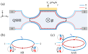
In this work, we investigate coherent electron transport through an Aharonov-Bohm (AB) interferometer composed of edge states; see Fig. 1(a). By imposing a random gate to the interferometer, the main -period AB oscillation is suppressed due to the dephasing effect [cf. Fig. 1(b)], giving rise to a dominant Al’tshuldr-Aronov-Spivak (AAS) oscillation with periodicity [cf. Fig. 1(c)]. Different from the conventional AAS oscillation, here, the weak antilocalization effect is induced by the random gate rather than disorder averaging Al’Tshuler et al. (1981); Al’tshuler et al. (1982). The results are generally stabilized by the time-reversal symmetry, thus offering a robust signature of the helical spin texture that does not rely much on the sample details. Specifically, the AAS oscillation of the return probability takes the form . The absence of return probability at is attributed to the destructive AAS interference induced by the spin Berry phase accumulated during inter-edge tunneling, a direct result of the helical spin texture. For the trivial edge state, the return probability take the general form with , where the “” is determined by the strength of the spin-orbit coupling. In contrast to the helical edge states, nonzero return probability occurs at for the trivial edge states due to the doubling of transport channels. The different oscillation patterns of the return probability can be measured by the differential conductance. Therefore, our scheme provides an unambiguous evidence to discriminate between the nontrivial and trivial edge states.
The rest of this paper is organized as follows. In Sec. II, we explicate the basic physical picture of the main results. In Sec. III, we adopt a scattering matrix analysis based on the effective model of the edge states to solve the random gate induced -period oscillation of the return probability. Detailed numerical simulations on the lattice model is conducted in Sec. IV to show the robustness of the main results for the helical edge states. In Sec. V, we study the AAS oscillation for the trivial edge states and compare the results with that of the helical edge states. Finally, a brief summary and discussion are given in Sec. VI.
II Physical picture
The AB interferometer constructed by the edge states of the QSHI is illustrated in Fig. 1(a), where the spin up (down) edge states propagate in the clockwise (anticlockwise) direction. Two point contacts (PCs) are fabricated to introduce inter-edge coupling Strunz et al. (2020), such that the central region of the setup forms a closed interfering loop. A weak magnetic field is applied, which acts on the electron motion through the flux modulation in the area enclosed by the interference loop. At two PCs, Rashba spin-orbit coupling can be induced by local electric fields Rothe et al. (2010); Ström et al. (2010); Väyrynen and Ojanen (2011); Strunz et al. (2020), which gives rise to inter-edge transmission, i.e., electrons in one edge transmit to the opposite edge with the same moving direction accompanied by a spin flipping Väyrynen and Ojanen (2011); Chen et al. (2016). Here, we apply a gate voltage to the upper edge; see Fig. 1(a), which introduces an additional phase factor to the wave function of the upper electron, with the length of the gate and the velocity of the edge states. Here, takes random values, which is key to the main results of this work.
Consider an electron propagates coherently in the AB interferometer, which contains multiple interfering loops. Two typical ones among them are the main AB and AAS interfering loops, as shown in Figs. 1(b) and 1(c), respectively. The main AB loop is composed of the upper and lower transmission channels, which results in a -period oscillation of transmission probability. Such interference is sensitive to the phase shift induced by so that a random causes dephasing effect and quenches such AB oscillation. In contrast, the AAS interference consists of two backscattering trajectories being the time-reversal counterpart to each other. As the time scale of fluctuation is much larger than that an electron spends inside the interferometer, the pair of paths gain the same random phase . Therefore, such AAS interference survives, giving rise to a dominant -period oscillation of the return probability.
Importantly, the electron return probability contains the key information of the helical spin texture of the edge states. Consider an electron incident from terminal 1 in Fig. 1(a), both two backscattering trajectories involves an inter-edge transmission along with a spin rotation about the axis in opposite directions denoted by the rotation operator ; see Fig. 1(c). Accordingly, the backscattering wave function takes the form , with the backscattering amplitude for each path. It reduces to and gives rise to the probability using the property of the spin Berry phase . Since the spin rotation is enforced by the spin-momentum locking, such an oscillation behavior directly reveals the spin texture of the edge states. For zero magnetic field with , the return probability vanishes, which is prohibited by the time-reversal symmetry of the helical edge states. A small magnetic flux breaks the time-reversal symmetry and increases the return probability, indicating a weak antilocalization effect.
III Scattering matrix analysis
In this section, we study electron transport in the interferometer using the scattering matrix approach based on the low-energy model of the edge states. The scattering matrix of the whole interferometer is obtained by combining the scattering matrices at two PCs and involving the phase accumulation during electron propagation. The scattering matrix at the left PC can be parameterized as
| (1) |
which relates the incident and outgoing waves via . The four components of the wave correspond to the upper and lower channels on the left and right side of the PC. Here, the antisymmetric condition is taken into account due to the time-reversal symmetry of the helical states Bardarson and Moore (2013). The amplitudes are the intra- and inter-edge transmission, respectively; are the inter-edge reflection on both sides of the PC, while the intra-edge reflection with spin flipping is prohibited by the time-reversal symmetry. The matrix for the right PC is defined in the same way. The phase modulation of the interferometer comes from the gate voltage deposited on the upper channel [cf. Fig. 1(a)] and the flux in the middle area encircled by the interfering loop, which can be described by the matrix
| (2) |
where are the extra phase due to the magnetic field, with the sum being gauge invariant.
Combining three matrices yields the scattering matrix for the whole interferometer. In the following, is adopted for simplicity, which will not change the main results. For an electron injected from terminal 1, its return probability and transmission probability to terminal 2 are obtained after some algebra as
| (3) |
where , , , with are the arguments of , respectively, and .
The scattering probabilities in Eq. (3) contains the information of the competition between the AB and AAS effects. For a fixed or equivalently, the phase factor , the transmission is dominated by the AB oscillation with periodicity. Due to the current conservation, the -period component also appears in the oscillating pattern of the return probability . As takes random values or equivalently, it is integrated out, the first-order AB oscillation quenches and the -period AAS oscillation dominates the transport. This fact can be clearly seen in the weak reflection limit of the PCs, that is . By expanding in Eq. (3) to the first order of , the return probability reduces to
| (4) |
which contains both and periodicity. To see the effect due to the random gate voltage, we integrate out , which yields
| (5) |
where only the -period oscillation remains. Similarly, the averaged transmission probability reduces to
| (6) |
in which only the -period oscillation remains, the same as . The random introduces dephasing effect to the AB interference process while retains phase coherence between paired AAS interference loops. As a result, the AAS effect dominates the transport, giving rise to the -period oscillation.
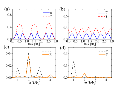
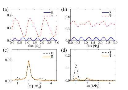
The conclusion above generally holds beyond the weak reflection limit. We provide numerical results of Eq. (3) for a general case in Fig. 2. The return and transmission probabilities for fixed and random are shown in Figs. 2(a) and 2(b), respectively. For a certain , the transmission is dominated by the AB oscillation with periodicity. As is averaged out, both and oscillate with periodicity, which is a clear signature of the AAS scenario. The transition of the oscillation period from (in ) to (in ) visibly manifests the random gate induced AAS interference. Importantly, here the return probability takes the form of which vanishes for . It is a direct result of the spin-momentum locking as elucidated in Sec. II thus providing a direct evidence of helical edge states.

IV Lattice model simulation
Based on the scattering matrix analysis, one can see that only the AAS oscillation is stable for a random . Next, we perform numerical simulation to show the robustness of the results. We adopt the Bernevig-Hughes-Zhang model to describe the QSHI Bernevig et al. (2006)
| (7) |
where and are Pauli matrices acting on the spin and orbital space, respectively. Here, , and are the material parameters. At the PC, the Rashba spin-orbit coupling is described by Rothe et al. (2010). We map the effective model onto the square lattice through the substitutions with the lattice constant (see Appendix A for details) and calculate the scattering probabilities using KWANT package Groth et al. (2014).
The geometric parameters of the setup are provided in the caption of Fig. 2 and Appendix A. The side gate voltage is applied on the upper edge states, specifically, in the area of the middle region. The strengths of Rashba spin-orbit coupling around two PCs are set to an equal value. Consider an electron injected from terminal 1 with an energy within the bulk gap of the QSHI, only the edge channels are available for propagation. The scattering probabilities for is shown in Fig. 2(c), which resemble those from the edge state analysis in Fig. 2(a). Specifically, is dominated by the -period oscillation and contains multiple periods of oscillation. Then we consider a random with uniform distribution meV. The averaged scattering probability and are shown in Fig. 2(d). Both and exhibit a dominant -period oscillation, which manifests a random gate induced AAS effect. Note that vanishes for , indicates the helical spin texture of the edge states. The transition of the oscillating period is more clearly revealed by the frequency distribution of the oscillating pattern in Figs. 2(e) and 2(f). One can see that there are three peaks at in the FFT spectra of with nearly equal amplitude for a fixed . The random enhances the component in the FFT spectra of while quenches other frequencies, corresponding to a -period AAS oscillation. For the transmission , it is initially dominated by the frequency corresponding to the -period AB oscillation. After random averaging, the AB oscillation of quenches, while the -period AAS frequency maintains and dominates the transport.
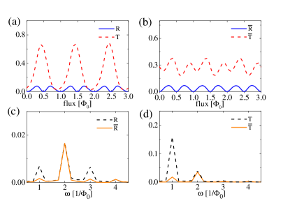
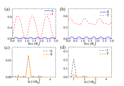
Next we show that the random gate induced AAS effect generally holds for different systemic parameters and is robust against nonmagnetic disorder. First, we change the Rashba coefficient at the right PC. The scattering probabilities () without (with) averaging are shown in Fig. 3. One can see that the main results still hold, i.e., the random quenches the -period oscillation and leads to a dominant -period oscillation as shown in Figs. 3(a) and 3(b). There are three peaks in the frequency domain of , and only a single peak at survives in after averaging; see Fig. 3(c). Accordingly, the -period AAS oscillation overwhelms the -period AB oscillation in the transmission probability as shown in Fig. 3 (d). Similar results also hold as one varies the length of the right PC as shown in Fig. 4. Fig. 5 shows the similar results with a different incident energy. The -period oscillation dominates the return probability ( and ) before and after averaging. The -period oscillation of the transmission probability is strongly suppressed by the random , while the component remains unaffected. We also show in Fig. 6 that our results are robust against disorder. Since the main results are stabilized by the time-reversal symmetry, the modification of the sample details will not change the qualitative results. From Figs. 3-6, one can see that the averaged return probability generally holds for various sample parameters, indicating the universality of the predicted signal of the helical edge states.
V Trivial edge states
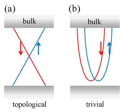
Very recently, trivial edge states have been reported in various QSHI candidates, which contribute similar conduction signature to that by the helical edge states Nguyen et al. (2016); Nichele et al. (2016); Mueller et al. (2017); Sazgari et al. (2019); de Vries et al. (2018, 2019). Thus, it is difficult to discriminate the two kinds of edge states with totally different physical origins. The main difference between the helical and trivial edge states can be seen in Fig. 7(a) and 7(b). The helical edge states originate from the band topology of QSHI, which cannot be realized in any one-dimensional nanowire. In contrast, the trivial edge states originate from the surface band bending without topological reasons Nichele et al. (2016), which resembles those of a nanowire with Rashba spin-orbit coupling Haidekker Galambos et al. (2020), as shown in Fig. 7(b). The trivial edge states differ from the helical ones by a doubling of the transport channel, in which backscattering with spin conservation becomes possible. Therefore, the existence of backscattering or not provides a distinctive signal for the identification of helical and trivial edge states, which can be probed in the oscillation pattern of the return probability.
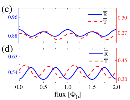
We simulate the trivial edge states by a one-dimensional nanowire with Rashba spin-orbit coupling described by the Hamiltonian . The AB and AAS effects are studied numerically in the interferometer composed of two nanowires coupling at two points based on the lattice model. A magnetic flux threads the closed loop and a gate voltage is imposed to the upper edge like that in the QSHI model. At the coupling bond between two nanowires, the Rashba spin-orbit coupling during lateral hopping is included. The oscillation patterns for and after averaging are plotted in Figs. 7(c) and 7(d). One can see that the averaged scattering probabilities exhibit a -period oscillation, indicating an AAS effect dominated scenario. Specifically, for a small Rashba coefficient, the return probability can be captured by ; see Fig. 7(c). A small magnetic field results in a decrease of , showing the weak localization effect. For a large Rashba coefficient, the oscillation acquires an extra phase shift, i.e., as shown in Fig. 7(d), which is the weak antilocalization effect. The feature of pattern for the trivial edge states provides an effective way to discriminate them from helical edge states. As the oscillation of shows a weak localization behavior as that in Fig. 7(c), trivial edge states are confirmed. Importantly, in both weak localization and antilocalization regimes of the trivial edge states, the return probability is always finite for , in start contrast to the helical edge states, thus providing a discriminative signal of the helical and trivial edge states.
VI Discussion and Summary
Some remarks are made below about the experimental implementation of our proposal. The main ingredient of the interferometer is the PC structure introducing inter-edge coupling which can be achieved by state-of-the-art fabrication techniques Strunz et al. (2020). Then two PCs make up an interferometer giving rise to coherent oscillation of the scattering probabilities with varying magnetic field. The distinctive signature of helical and trivial edge states can be extracted from the oscillation pattern of the return probability , which is directly related to the differential conductance by . Specifically, as the oscillation of exhibits a weak localization scenario, trivial edge states can be identified. If shows a weak antilocalization oscillation, the helical and trivial edge states can be discriminated by zero and finite at , respectively. Note that the precondition for such a judgement is the occurrence of coherent oscillation. In our proposal, the absence of return probability should originate from a spin-texture resolved interference effect rather than other trivial physical reasons. The averaged return probability by AAS interference further reveals the robustness and universality of such a signal, which excludes any accidental result by fine tuning the parameters.
To summarize, we investigate quantum coherent transport through an AB interferometer constructed by the edge states of a QSHI. By applying a random gate to the edge channel, the -period AB oscillation quenches and the -period AAS oscillation dominates the transport. Such random gate induced AAS oscillation differs from the conventional scenario of disorder averaging. The helical spin texture of topological edge states results in an AAS oscillation of the weak antilocalization type and more importantly the absence of return probability at zero magnetic field. In contrast, the AAS oscillation for the trivial edge states can be of either weak localization or antilocalization type, both having nonzero return probability. Therefore, our proposal provides an effective way for the discrimination between helical and trivial edge states through spin resolved interference effect. Such a signal is protected by time-reversal symmetry, so that it generally holds without fine tuning of the system and is robust against disorder.
Acknowledgements.
This work was supported by the National Natural Science Foundation of China under Grant No. 12074172 (W.C.), No. 11674160 and No. 11974168 (L.S.), the startup grant at Nanjing University (W.C.), the State Key Program for Basic Researches of China under Grants No. 2017YFA0303203 (D.Y.X.) and the Excellent Programme at Nanjing University.Appendix A Lattice model for numerical calculation
In this Appendix, we elucidate the parameters for the interferometer sketched in Fig. 1(a). The hard-wall boundary in the direction is described by the following function
| (8) |
where is the width of the lead, and are the width and length of PC.
The whole devices can be described by Hamiltonian , where is the Hamiltonian of QSHI and is the Hamiltonian of SOC. Here, we use HgTe/CdTe quantum wells in our proposal, which can be described by Bernevig-Hughes-Zhang model as
where and are Pauli matrices of spin and orbital respectively. , , , and . A, B, D and M are the material parameters which can be controlled by experiment. The Hamiltonian of SOC is
where is Rashba coefficient.
In order to run numerical calculations, we use a square lattice model for whole system by discretizing the continuous effective hamiltonian . By using , , , we can derive the Hamiltonian to real space. The lattice Hamiltonian is
| (9) |
where are the annihilate operators of electron with spin up and spin down in s and p orbits at site i. The , and are 4 4 Hamiltonians,
| (10) |
where lattice constant is nm.
References
- Qi and Zhang (2011) X.-L. Qi and S.-C. Zhang, Rev. Mod. Phys. 83, 1057 (2011).
- Hasan and Kane (2010) M. Z. Hasan and C. L. Kane, Rev. Mod. Phys. 82, 3045 (2010).
- Kane and Mele (2005) C. L. Kane and E. J. Mele, Phys. Rev. Lett. 95, 226801 (2005).
- Bernevig and Zhang (2006) B. A. Bernevig and S.-C. Zhang, Phys. Rev. Lett. 96, 106802 (2006).
- Bernevig et al. (2006) B. A. Bernevig, T. L. Hughes, and S.-C. Zhang, Science 314, 1757 (2006).
- Liu et al. (2008) C. Liu, T. L. Hughes, X.-L. Qi, K. Wang, and S.-C. Zhang, Phys. Rev. Lett. 100, 236601 (2008).
- König et al. (2007) M. König, S. Wiedmann, C. Brüne, A. Roth, H. Buhmann, L. W. Molenkamp, X.-L. Qi, and S.-C. Zhang, Science 318, 766 (2007).
- Knez et al. (2011) I. Knez, R.-R. Du, and G. Sullivan, Phys. Rev. Lett. 107, 136603 (2011).
- Knez et al. (2014) I. Knez, C. T. Rettner, S.-H. Yang, S. S. P. Parkin, L. Du, R.-R. Du, and G. Sullivan, Phys. Rev. Lett. 112, 026602 (2014).
- Du et al. (2015) L. Du, I. Knez, G. Sullivan, and R.-R. Du, Phys. Rev. Lett. 114, 096802 (2015).
- Fu and Kane (2008) L. Fu and C. L. Kane, Phys. Rev. Lett. 100, 096407 (2008).
- Fu and Kane (2009) L. Fu and C. L. Kane, Phys. Rev. B 79, 161408 (2009).
- Kitaev (2001) A. Y. Kitaev, Physics-Uspekhi 44, 131 (2001).
- Nguyen et al. (2016) B.-M. Nguyen, A. A. Kiselev, R. Noah, W. Yi, F. Qu, A. J. A. Beukman, F. K. de Vries, J. van Veen, S. Nadj-Perge, L. P. Kouwenhoven, M. Kjaergaard, H. J. Suominen, F. Nichele, C. M. Marcus, M. J. Manfra, and M. Sokolich, Phys. Rev. Lett. 117, 077701 (2016).
- Nichele et al. (2016) F. Nichele, H. J. Suominen, M. Kjaergaard, C. M. Marcus, E. Sajadi, J. A. Folk, F. Qu, A. J. A. Beukman, F. K. de Vries, J. van Veen, S. Nadj-Perge, L. P. Kouwenhoven, B.-M. Nguyen, A. A. Kiselev, W. Yi, M. Sokolich, M. J. Manfra, E. M. Spanton, and K. A. Moler, New Journal of Physics 18, 083005 (2016).
- Mueller et al. (2017) S. Mueller, C. Mittag, T. Tschirky, C. Charpentier, W. Wegscheider, K. Ensslin, and T. Ihn, Phys. Rev. B 96, 075406 (2017).
- Sazgari et al. (2019) V. Sazgari, G. Sullivan, and i. d. I. i. d. I. Kaya, Phys. Rev. B 100, 041404 (2019).
- de Vries et al. (2018) F. K. de Vries, T. Timmerman, V. P. Ostroukh, J. van Veen, A. J. A. Beukman, F. Qu, M. Wimmer, B.-M. Nguyen, A. A. Kiselev, W. Yi, M. Sokolich, M. J. Manfra, C. M. Marcus, and L. P. Kouwenhoven, Phys. Rev. Lett. 120, 047702 (2018).
- de Vries et al. (2019) F. K. de Vries, M. L. Sol, S. Gazibegovic, R. L. M. o. h. Veld, S. C. Balk, D. Car, E. P. A. M. Bakkers, L. P. Kouwenhoven, and J. Shen, Phys. Rev. Research 1, 032031 (2019).
- Hou et al. (2009) C.-Y. Hou, E.-A. Kim, and C. Chamon, Phys. Rev. Lett. 102, 076602 (2009).
- Schmidt (2011) T. L. Schmidt, Phys. Rev. Lett. 107, 096602 (2011).
- Das and Rao (2011) S. Das and S. Rao, Phys. Rev. Lett. 106, 236403 (2011).
- Soori et al. (2012) A. Soori, S. Das, and S. Rao, Phys. Rev. B 86, 125312 (2012).
- Edge et al. (2013) J. M. Edge, J. Li, P. Delplace, and M. Büttiker, Phys. Rev. Lett. 110, 246601 (2013).
- Romeo and Citro (2014) F. Romeo and R. Citro, Phys. Rev. B 90, 155408 (2014).
- Chen et al. (2016) W. Chen, W.-Y. Deng, J.-M. Hou, D. N. Shi, L. Sheng, and D. Y. Xing, Phys. Rev. Lett. 117, 076802 (2016).
- Al’Tshuler et al. (1981) B. Al’Tshuler, A. Aronov, and B. Spivak, Jetp Lett 33, 94 (1981).
- Al’tshuler et al. (1982) B. Al’tshuler, A. Aronov, B. Spivak, D. Y. Sharvin, and Y. V. Sharvin, JETP Lett 35, 588 (1982).
- Strunz et al. (2020) J. Strunz, J. Wiedenmann, C. Fleckenstein, L. Lunczer, W. Beugeling, V. L. Müller, P. Shekhar, N. T. Ziani, S. Shamim, J. Kleinlein, et al., Nature Physics 16, 83 (2020).
- Rothe et al. (2010) D. Rothe, R. Reinthaler, C. Liu, L. Molenkamp, S. Zhang, and E. Hankiewicz, New Journal of Physics 12, 065012 (2010).
- Ström et al. (2010) A. Ström, H. Johannesson, and G. Japaridze, Physical review letters 104, 256804 (2010).
- Väyrynen and Ojanen (2011) J. I. Väyrynen and T. Ojanen, Physical review letters 106, 076803 (2011).
- Bardarson and Moore (2013) J. H. Bardarson and J. E. Moore, Reports on Progress in Physics 76, 056501 (2013).
- Groth et al. (2014) C. W. Groth, M. Wimmer, A. R. Akhmerov, and X. Waintal, New Journal of Physics 16, 063065 (2014).
- Haidekker Galambos et al. (2020) T. Haidekker Galambos, S. Hoffman, P. Recher, J. Klinovaja, and D. Loss, Phys. Rev. Lett. 125, 157701 (2020).