Representation and design of wavelets using unitary circuits
Abstract
The representation of discrete, compact wavelet transformations (WTs) as circuits of local unitary gates is discussed. We employ a similar formalism as used in the multi-scale representation of quantum many-body wavefunctions using unitary circuits, further cementing the relation established in Refs. MattWavelet, ; waveMERA, between classical and quantum multi-scale methods. An algorithm for constructing the circuit representation of known orthogonal, dyadic, discrete WTs is presented, and the explicit representation for Daubechies wavelets, coiflets, and symlets is provided. Furthermore, we demonstrate the usefulness of the circuit formalism in designing novel WTs, including various classes of symmetric wavelets and multi-wavelets, boundary wavelets and biorthogonal wavelets.
pacs:
05.30.-d, 02.70.-c, 03.67.Mn, 75.10.JmI Introduction
The development of compact, orthogonal waveletsDaub1 ; Daub2 ; Daub3 ; Daub4 represents one of the most significant advances in signal processing from recent timesWaveBook1 ; WaveBook2 ; WaveBook3 . Like well established methods based on Fourier analysis, wavelets can be employed to obtain a compressed representation of spatially or temporally correlated data, and thus have found significant applications in image, audio and video compression WaveImageApp ; SigBook ; JPEG . By providing a multi-resolution analysis, a WT can capture correlations over many different length/time scales, which is key to their usefulness in practical applications.
Similarly, multi-scale methods, in the context of the renormalization group (RG) RGreview , which provides a systematic framework to implement changes of scale in many body systems, have also had a long and successful history in the context of condensed matter physics and quantum field theories. A recent advance in RG methods for quantum many-body systems is the multi-scale entanglement renormalization ansatz (MERA)ER ; MERA , where quantum many-body wavefunctions are represented as circuits comprised of local unitary gates. By properly encoding correlations at all length scales, MERA have been demonstrated to be particularly useful in the numerical investigation of quantum many-body systems where many scales of length are important, such as in systems at the critical point of a phase transitionMERAlocal ; MERAnonlocal ; MERAbook ; Alg2 ; MERAapp1 ; MERAapp2 ; MERAapp3 ; MERAapp4 .
While the conceptual links between WTs and the RG have been previously examinedBattle , more recently it was shown that a WT acting in the space of fermionic mode operators corresponds precisely to a MERAMattWavelet ; waveMERA . This wavelet/MERA connection proved useful in allowing construction of the first known analytic MERA for a critical system, and may further prove useful in understanding e.g. the scaling of errors in MERA. The purpose of this paper is to take the connection the other way, and examine whether the tools and ideas developed in the context of the MERA are useful in the understanding and design of WTs. Specifically, we discuss the use of unitary circuits for the representation of standard families of dyadic wavelets (including Daubechies wavelets, coiflets and symlets), and then explore use of unitary circuits for the design of novel wavelet families (including symmetric wavelets of dilation factor and , symmetric multiwavelets, boundary wavelets, and a new family of symmetric biorthogonal wavelets).
This paper is organized as follows. Firstly in Sect. II we introduce our notion of multi-scale unitary circuits, which follow as the classical analogue of MERA quantum circuits. Then in Sect. III we discuss the representation of discrete, orthogonal, dyadic wavelet transformations as unitary circuits. This includes providing the explicit form of the circuit representation for Daubechies wavelets, coiflets and symlets, as well as an algorithm for obtaining the circuit representation of arbitrary dyadic wavelets. In Sect. IV we explore the use of generalized unitary circuits in the design of novel WTs, including, in Sect. IV.1 families of symmetric dilation factor wavelets, in Sect. IV.2 a family of symmetric multiwavelets, in Sect. IV.3 a family of symmetric dilation factor wavelets, in Sect. IV.4 a construction of boundary wavelets, and in Sect. IV.5 a family of symmetric biorthogonal wavelets. Finally, conclusions and discussion are presented in Sect. V.
II Unitary Circuits
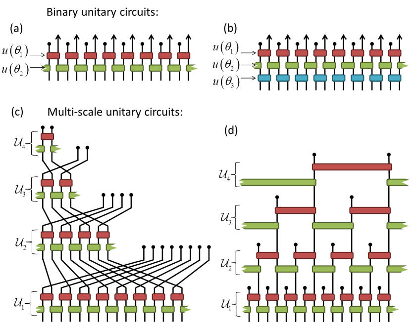
In this section we define our notions of binary and multi-scale unitary circuits, with are the analogue of the MERA circuitsMERA used for representing quantum many-body wavefunctions. Let be a unitary matrix for integer . We say is a binary unitary circuit of depth if it can be written as a product of matrices ,
| (1) |
where each is a unitary matrix that is the direct sum of neighboring unitary matrices (alternating between odd-even and even-odd placement with each layer), i.e. such that
| (2) |
for odd, and with the direct sum over even sites for even, see also Fig. 1(a-b) for a diagrammatic representation. The free parameter defines an angle of rotation in the unitary matrix ,
| (5) | ||||
| (8) |
where is short for .
A multi-scale circuit, representing a matrix of dimension for positive integer , can be formed from composition of binary unitary circuits,
| (9) |
Here each is a binary unitary circuit of linear dimension and the composition is such that acts only on the even index sites of the previous , see also Fig. 1(c-d).
III Wavelets and unitary circuits
In this section we describe how discrete WTs can be represented as unitary circuits, first in Sect. III.1 recalling basic properties of wavelets WaveBook2 , before next in Sect. III.2 providing a specific example of the circuit representation of the D4 Daubechies wavelet, and finally in Sect. III.3 providing an algorithm for constructing the circuit representation of arbitrary dyadic orthogonal wavelets.
III.1 Basic properties of orthogonal wavelets
Here we recall the fundamentals of compact, dyadic (i.e. dilation factor ), orthogonal wavelets. We seek to construct a set of wavelet functions for on a lattice of sites, where denotes the scale over which the function has non-zero support, such that wavelet has a compact support of sites. Additionally, we require that wavelets at different scales should be mutually orthogonal, and wavelets at the same scale should be orthogonal under translations of sites for integer . The construction of wavelets that fulfill these properties is facilitated by first introducing the set of scaling functions, which we denote for , where again denotes scale. The scaling functions are defined recursively through the refinement equation WaveBook3 ,
| (10) |
where is called the scaling sequence, with the order of the wavelet transform. Note that the scaling function at smallest scale is defined directly from the scaling sequence, , with the Kronecker delta function. A necessary condition for a scaling sequence to generate orthogonal wavelets is that it is orthogonal to itself under shifts by an even number of coefficients,
| (11) |
For dyadic wavelets, the wavelet sequence is defined from the scaling sequence by reversing the order of elements and introducing an alternating minus sign,
| (12) |
Notice that the wavelet sequence is, by construction, orthogonal to the scaling sequence from which it is derived. The wavelets can now be defined from the scaling functions; specifically the wavelet at scale is given from linear combinations of translations of scaling functions at the previous scale,
| (13) |
Following this recipe, any scaling sequence that satisfies the orthogonality constraints of Eq. 11 can be applied to generate a set of wavelet functions for , which can be argued to form a complete and orthogonal basis for the lattice.
In order to realize a wavelet transform that resolves high/low frequencies at each scale additional constraints are imposed on the wavelet sequence , where the specific constraints may depend on the family of wavelets under consideration. For Daubechies wavelets with scaling sequence of coefficients, denoted D2N wavelets, it is imposed that the first moments of the wavelet sequence should vanish, i.e. that
| (14) |
for .
III.2 Circuit representation of Daubechies D4 wavelets
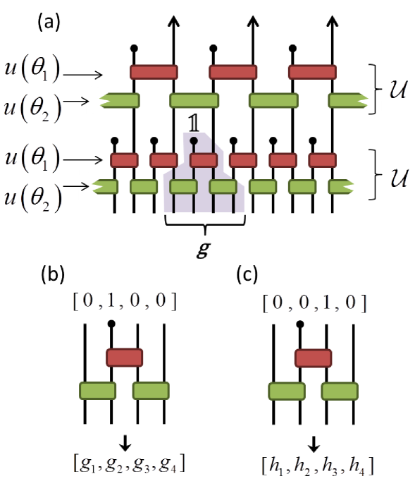
We now provide an example of how the Daubechies D4 wavelets, which are characterized by the scaling sequence , can be encoded as a binary unitary circuit of depth . More precisely, we show that the angles that define the circuit can be chosen such that the scaling sequence of the D4 wavelets is reproduced when transforming the unit vector on any odd site ,
| (15) |
where the brackets indicate that we only take the part of the vector with non-zero support, and ‘’ indicates standard matrix multiplication. Only a few of the local unitary gates from contribute to this non-zero support, see also Fig. 2, such that Eq. 15 may be equivalently expressed as,
| (16) |
with ‘’ representing the direct sum. This expression can be evaluated in terms of the tangent angles and , see Eq. 8, that parameterize the local unitary matrices and respectively,
| (33) | ||||
| (38) |
Note that, for simplicity, we have neglected an overall normalization factor from the contributions in Eq. 8. Similarly the wavelet sequence , which follows from transforming the unit vector on any even site , is given as,
| (39) |
which evaluates to,
| (40) |
Notice that and satisfy the relation between wavelet and scaling sequences prescribed in Eq. 12 for any choice of the angles . Substituting this parameterization for into Eq. 14 for moments gives,
| (41) |
These equations are satisfied for the tangent angles,
| (42) |
which gives the angles that parameterize the unitary circuit,
| (43) |
Substituting these values in Eqs. 38 and 40 for scaling and wavelet sequences (when normalized to unity) yields,
| (44) |
which equates to the known D4 sequences Daub1 .
III.3 Circuit representation of generic dyadic wavelets
We now describe how to construct the unitary circuit representation for generic (compact, orthogonal, dyadic) wavelet transformations. Let be a binary unitary circuit of depth , which is parameterized by the set of angles . We associate scaling and wavelet sequences of coefficients to the (non-zero support of the) transformation of the unit vector on odd or even sites,
| (45) | ||||
| (46) |
We shall argue the following:
- 1.
- 2.
Notice it follows trivially that the scaling coefficient sequences from unitary circuits satisfy the orthogonality constraints of Eq. 11, as shifts of the scaling sequence correspond to different columns of the unitary matrix . In Sect. III.3.1 we offer a proof that and satisfy the relation of Eq. 12, while in Sect. III.3.2 we describe an algorithm that, for any scaling sequence , generates the set of angles that parameterizes a depth unitary circuit that encodes the sequence. Together these two results prove statement 1 above. Statement 2 then follows easily, as the composition of binary unitary circuits, described in Eq. 9 and depicted in Fig. 1(c), is clearly seen to be equivalent to the refinement equation of Eq. 10.
III.3.1 Relation between scaling and wavelet sequences
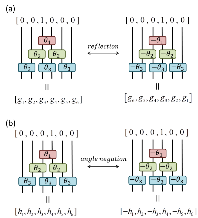
Here we offer a proof that scaling and wavelet sequences from unitary circuits always satisfy the relation of Eq. 12. We begin by defining the spatial reflection operator which reverses the order of both rows and columns of a matrix, i.e if for a given matrix we have that then the matrix elements of and are related as
| (47) |
Notice that spatial reflection of a unitary from Eq. 8 changes the sign of the angle ,
| (48) |
It follows that, if is a binary unitary circuit parameterized by angles , then its spatial reflection is a binary unitary circuit with opposite sign angles . Notice that spatial reflection of circuit into has exchanged the role of the scaling and wavelet sequences, such that if is the wavelet sequence of and is the scaling sequence of , then
| (49) |
see also Fig. 3(a). Thus in order to demonstrate the relation between and of Eq. 12, it suffices to show that the elements of and are related with an alternating negative sign,
| (50) |
see also Fig. 3(b), which we now prove.
Consider the factorization of the circuit into its constituent layers,
| (51) |
where each is a function of some . Let and be vectors of length for integer , and assume . Define as given by the transform by circuit layer ,
| (52) |
and as given by the transform of by a layer of opposite sign,
| (53) |
If it can be shown that then Eq. 50 follows from recursion over all layers of the binary circuit ; in order to show this we evaluate elements of from Eq. 52,
| (60) | ||||
| (63) |
and similarly evaluate elements from Eq. 53,
| (70) | ||||
| (73) | ||||
| (76) | ||||
| (79) |
from which the desired result is observed. Thus we conclude that the scaling and wavelet sequences from a binary unitary circuit are always related as per Eq. 12.
III.3.2 Circuit construction algorithm
Given a discrete, orthogonal WT described by the scaling sequence of coefficients, we now describe an algorithm to encode the sequence as a depth binary unitary circuit. More precisely, we describe how the angles defining the circuit can be uniquely chosen such that the scaling sequence is mapped to a unit vector under transformation by the circuit,
| (80) |
in accordance with the definition of Eq. 45. Recall that the binary circuit decomposes into layers, , where each layer is the direct sum of a unitary matrices . Let be the scaling sequence after transforming by the bottom layer of the unitary circuit,
| (81) |
We now propose that the free angle of unitary should be chosen as,
| (82) |
Under this choice the first element of the transformed scaling sequence is zero,
| (83) |
for all three possibilities (i-iii) from Eq. 82. To understand this in the second instance (ii) notice that the orthogonality constraints of Eq. 11 impose,
| (84) |
which implies that given that . Similarly, the trailing element of is also mapped to zero,
| (85) |
In instances (ii) and (iii) from Eq. 82 this follows trivially, whereas in the first instance (i) this can be understood by substituting the orthogonality constraint of Eq. 11 to give,
| (86) |
Thus we have demonstrated that under the choice of angle from Eq. 82 the scaling sequence of coefficients is mapped under to a new sequence of coefficients (where the first and last elements of , which were shown to be zero, have been dropped). It can also easily be seen that the orthogonality constraints on , see Eq. 11, map to an equivalent set of constraints for the new sequence . The set of angles is obtained by iterating this procedure a total of times, i.e. for unitary layers , which then maps the initial scaling sequence of coefficients into a sequence of length two denoted . At this stage, the angle associated to the top level is fixed at,
| (87) |
such that is mapped to a sequence with only a single non-zero element, indicating that the scaling sequence is encoded in the binary unitary circuit.
Employing this algorithm we generate the sets of angles that describe the Daubechies wavelets D2N for , see Tab. 1, the symlets of coefficients for , see Tab. 2, and the coiflets of coefficients for , see Tab. 3. Notice that clear patterns are evident in the angles between different orders of wavelets in each of the families, see also Fig. 4.
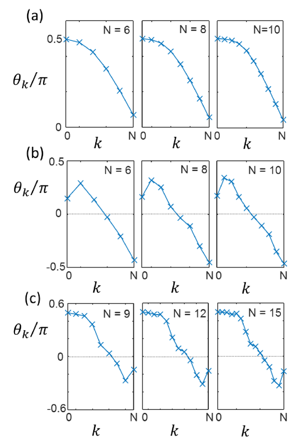
| D2 | D4 | D6 | D8 | D10 | D12 | D14 | D16 | D18 | D20 | |
|---|---|---|---|---|---|---|---|---|---|---|
| 1/4 | 5/12 | 0.466419 | 0.485368 | 0.493368 | 0.496925 | 0.498553 | 0.499312 | 0.499671 | 0.499841 | |
| - | 1/6 | 0.340895 | 0.419242 | 0.457854 | 0.477754 | 0.488217 | 0.493760 | 0.496701 | 0.498260 | |
| - | - | 0.124476 | 0.283112 | 0.372126 | 0.424117 | 0.455055 | 0.473548 | 0.484560 | 0.491068 | |
| - | - | - | 0.099238 | 0.240141 | 0.330420 | 0.389528 | 0.428559 | 0.454286 | 0.471103 | |
| - | - | - | - | 0.082499 | 0.207731 | 0.295133 | 0.357027 | 0.401092 | 0.432370 | |
| - | - | - | - | - | 0.070599 | 0.182705 | 0.265668 | 0.327768 | 0.374473 | |
| - | - | - | - | - | - | 0.061708 | 0.162913 | 0.241041 | 0.301941 | |
| - | - | - | - | - | - | - | 0.054813 | 0.146919 | 0.220319 | |
| - | - | - | - | - | - | - | - | 0.049309 | 0.133750 | |
| - | - | - | - | - | - | - | - | - | 0.044815 |
| 1/4 | 5/12 | 0.466419 | 0.128000 | 0.197549 | 0.149210 | 0.418681 | 0.162192 | 0.207549 | 0.171178 | |
| - | 1/6 | 0.340895 | 0.213974 | -0.086984 | 0.289866 | -0.195828 | 0.323040 | -0.481080 | 0.343162 | |
| - | - | 0.124476 | -0.045343 | 0.279718 | 0.138289 | 0.068910 | 0.252744 | -0.018742 | 0.308034 | |
| - | - | - | -0.381317 | 0.076487 | -0.028270 | 0.498795 | 0.071840 | 0.380963 | 0.163525 | |
| - | - | - | - | -0.237764 | -0.204970 | -0.277830 | -0.032859 | 0.331334 | 0.059282 | |
| - | - | - | - | - | -0.429066 | 0.038275 | -0.112982 | 0.180695 | -0.027548 | |
| - | - | - | - | - | - | 0.381482 | -0.299591 | 0.086208 | -0.104053 | |
| - | - | - | - | - | - | - | -0.449411 | -0.091644 | -0.185998 | |
| - | - | - | - | - | - | - | - | -0.367415 | -0.351975 | |
| - | - | - | - | - | - | - | - | - | -0.460675 |
| 0.432513 | 0.486012 | 0.497096 | 0.499363 | 0.499855 | |
| 0.115026 | 0.449082 | 0.478861 | 0.494102 | 0.498385 | |
| -0.067486 | 0.293308 | 0.462006 | 0.474920 | 0.491529 | |
| - | 0.036930 | 0.365035 | 0.471844 | 0.472624 | |
| - | -0.163110 | 0.132236 | 0.401463 | 0.479637 | |
| - | -0.119802 | 0.040847 | 0.216145 | 0.423857 | |
| - | - | -0.080093 | 0.091539 | 0.274343 | |
| - | - | -0.267867 | 0.053920 | 0.139303 | |
| - | - | -0.144368 | -0.041439 | 0.111993 | |
| - | - | - | -0.209282 | 0.038183 | |
| - | - | - | -0.308590 | -0.041666 | |
| - | - | - | -0.159473 | -0.122667 | |
| - | - | - | - | -0.278205 | |
| - | - | - | - | -0.332208 | |
| - | - | - | - | -0.170007 |
IV Circuit constructions of novel wavelets
In the remainder of this manuscript we discuss the use of generalized unitary circuits for the design and realization of novel wavelet families. This includes families of (dilation factor ) symmetric wavelets in Sect. IV.1, symmetric multiwavelets in Sect. IV.2, a family of (dilation factor ) symmetric wavelets in Sect. IV.3, boundary wavelets in Sect. IV.4, and symmetric biorthogonal wavelets in Sect. IV.5. Many of the generalized circuits considered are direct analogues of circuits considered previously in the context of MERA for quantum many-body systems (for instance, of the reflection symmetric MERA considered in Refs. MERAapp1, ; MERAapp2, , of the MERA of different dilation factors considered in Refs. MERAbook, ; Alg, , and of the boundary MERA considered in Refs. BoundMERA1, ; BoundMERA2, ).
IV.1 Dilation symmetric wavelets
An often desirable characteristic of wavelets is symmetry (or antisymmetry) under spatial reflections. However it is known that the only compactly supported orthogonal wavelet basis of dilation factor that consists of symmetric (or antisymmetric) functions is the trivial Haar basisDaub1 ; Daub2 . One solution to this problem is to use a larger dilation factor , which results in a scheme with one scaling and wavelet functions. Constructions of wavelets with larger dilation factors have been studied extensively in previous works, see for instance Refs. Sym1, ; Sym2, ; Sym3, ; Sym4, . In this Section we consider the design of novel symmetric (and/or antisymmetric) wavelets with dilation factor .
In the context of MERA quantum circuits, reflection symmetry (and, more generally, other spatial symmetries as well as global internal symmetries), are imposed by requiring that the individual unitary gates that comprise the circuit satisfy the symmetryMERAapp1 ; MERAapp2 . Here we follow a similar strategy, and construct reflection symmetric wavelets using unitary circuits where all of the unitary matrices that comprise the circuit are individually symmetric under spatial reflections. For unitary matrices, there is only a single non-trivial instance of a matrix, which we denote , that is invariant under reflections (as defined in Eq. 47),
| (88) |
which simply enacts a swap of elements on a length vector. For unitary matrices, a 1-parameter family of reflection symmetric matrices is obtained by exponentiating the most general instance of a real skew-hermitian matrix that is also reflection symmetric,
| (89) |
which evaluates to,
| (90) |
We now describe how to build a unitary circuit from these reflection symmetric matrices in conjunction with the swap gate , that will subsequently be used to parameterize a family of symmetric wavelet transforms with dilation factor .
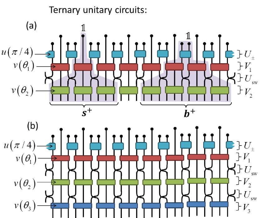
IV.1.1 Ternary unitary circuits
Let be a matrix for integer ; we say that is a ternary unitary circuit of depth if it can be decomposed as,
| (91) |
see also the circuit diagram of Fig. 5. Here each of the sublayers is a direct sum of matrices from Eq. 90,
| (92) |
which are interspersed with sublayers consisting of direct sums of swap gates from Eq. 88,
| (93) |
with the identity. The ternary circuit includes a top sublayer composed of unitary gates which are spaced by contributions of the identity,
| (94) |
Notice that the ternary unitary circuit of depth is fully parameterized by the set of angles . There are three coefficient sequences associated to a ternary circuit (which corresponds to a three-channel filter bank), which we label . Each of the three sequences is obtained by transforming a unit vector on different sites with the ternary circuit ,
| (95) |
see also Fig. 5. The sequences possess the following properties:
-
•
is a site-centered symmetric sequence of (odd) length elements (i.e. that is symmetric w.r.t. reflections about its central element)
-
•
is a edge-centered symmetric sequence of (even) length elements (i.e. that is symmetric w.r.t. reflections centered between its two central elements)
-
•
is a edge-centered antisymmetric sequence of (even) length elements (i.e. that is antisymmetric w.r.t. reflections centered between its two central elements).
Similar to the construction applied to the binary unitary circuit in Sect. II, layers of the ternary circuit can be composed to form a multi-scale circuit,
| (96) |
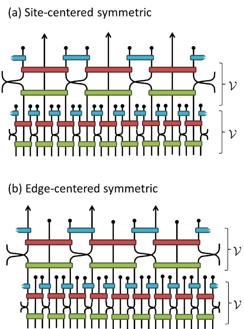
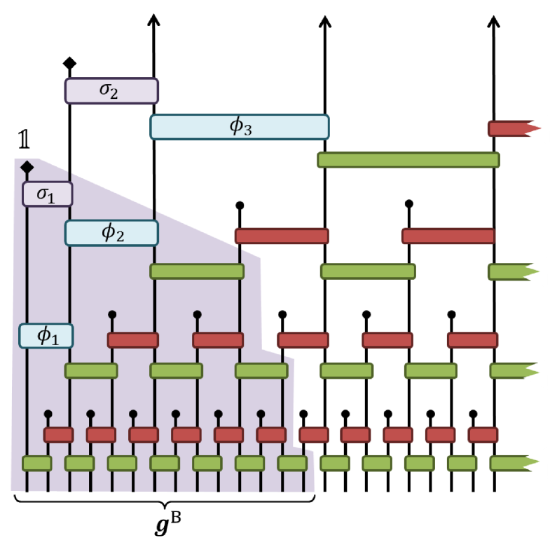
which encodes the dilation factor 3 discrete WT. Notice that there are two distinct ways of implementing this composition dependent on whether or is considered as the scaling sequence, which we refer to as the site-centered or edge-centered multi-scale circuits respectively, see also Fig. 6.
IV.1.2 Example 1: dilation wavelets with maximal vanishing moments
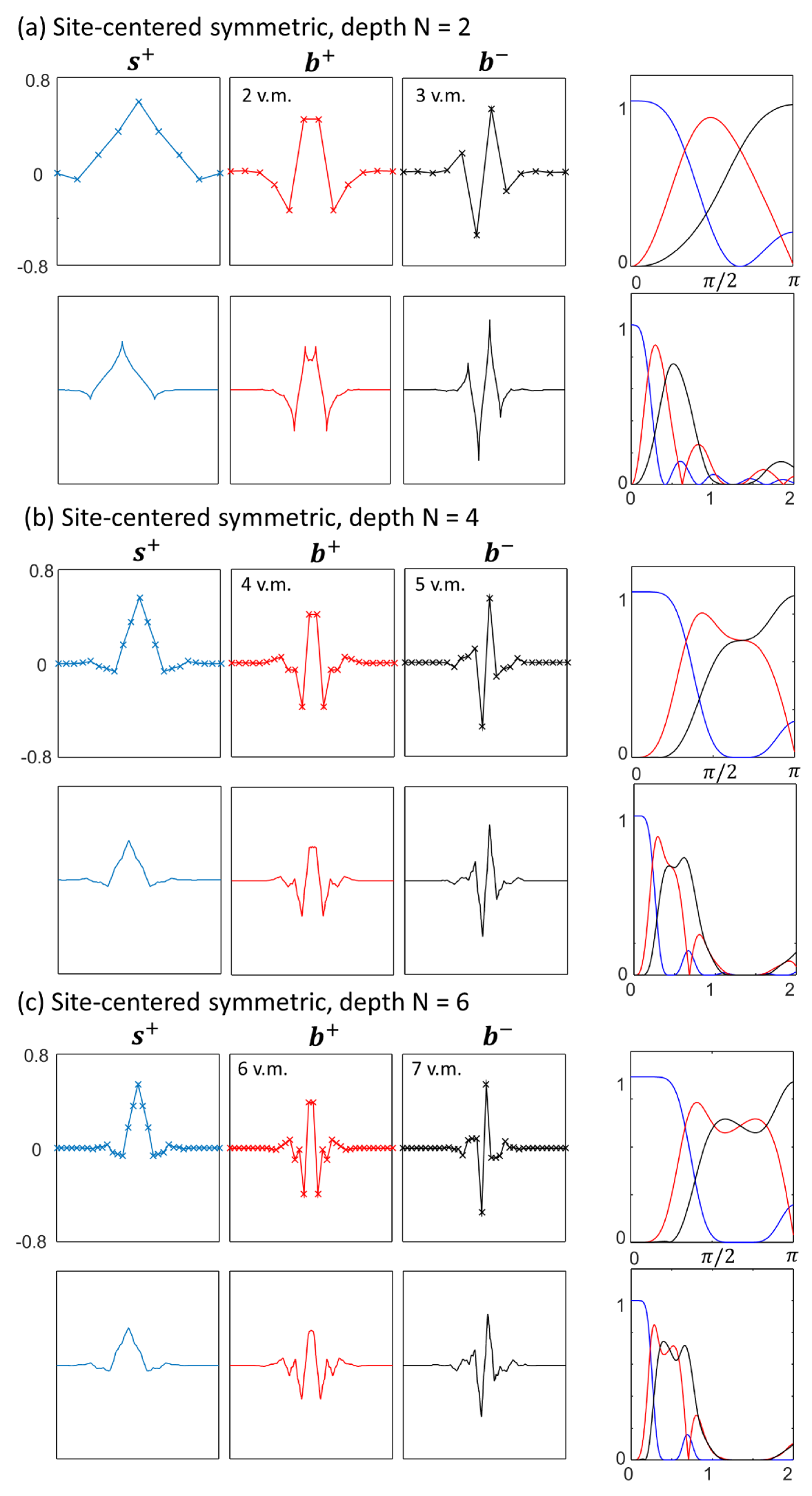
A depth ternary unitary circuit offers a parameterization of exactly reflection symmetric and antisymmetric wavelets with free parameters . In this section we consider the family of wavelets that result from choosing these parameters to maximize the number of vanishing moments that the wavelets possess.
We use the site-centered form of the multi-scale circuit as depicted in Fig. 6(a), where sequence is treated as the scaling sequence and , are the wavelet sequences, and we optimize the angles such the wavelets have vanishing moments,
| (97) |
for . Notice that is automatically orthogonal to odd polynomials due to its symmetry, and similarly is automatically orthogonal to even polynomials. Thus satisfying Eq. 97 for orders , i.e. such that the wavelets have vanishing moments, requires non-trivial constraints to be met.
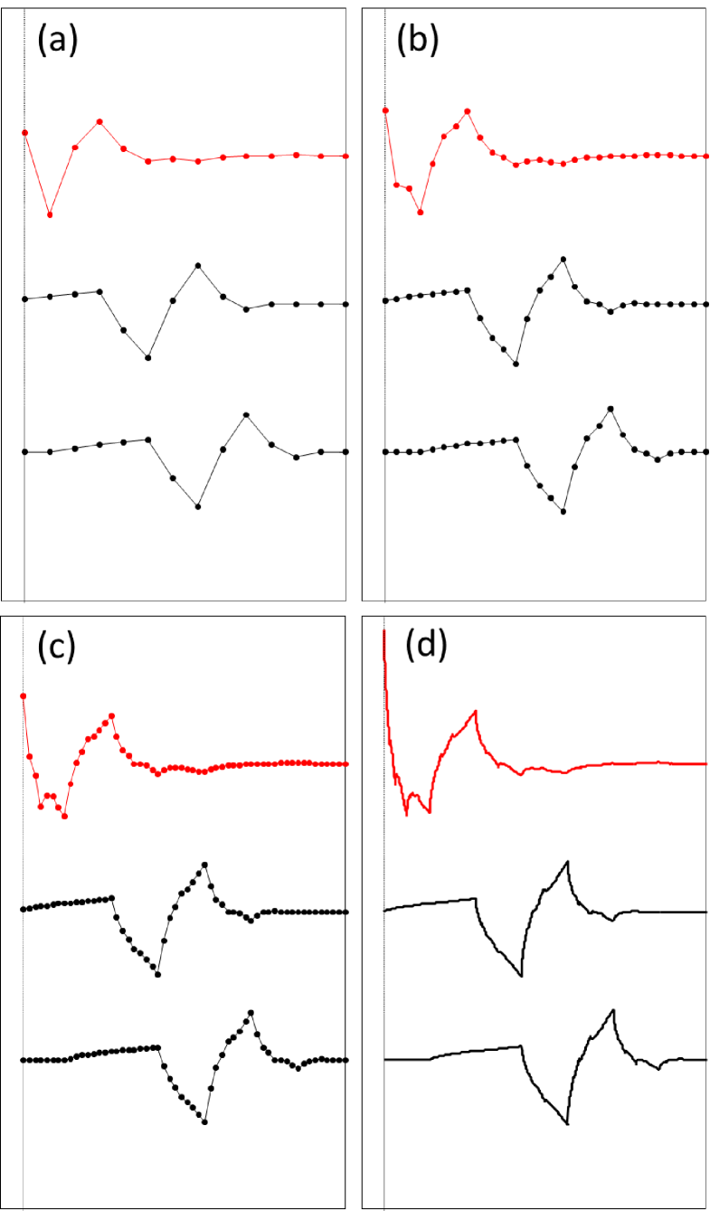
The sets of angles that satisfy the vanishing moment criteria for circuit depths are given in Tab. 4. These were obtained numerically using the standard Nelder-Mead algorithm to minimize the cost function given by the sum of the first moments of the wavelet sequences. The resulting wavelets are depicted in Fig. 7. Interestingly, while the scaling functions associated to these WTs appear similar to those obtained previously in Figs. 3 and 5 of Ref. Sym1, , the wavelets themselves are seen to have much smaller effective support (i.e. the region over which the wavelets have non-vanishingly small amplitude is reduced), which suggests they may perform better in practical applications.
| 0.275642799 | 0.595157579 | 0.756972477 | |
| 0.679673818 | -0.840085482 | -1.401172929 | |
| - | -0.314805259 | 0.537202982 | |
| - | 1.515049781 | 0.264416395 | |
| - | - | -1.007834534 | |
| - | - | 1.805732227 |
| Type I |
|
|
|
||||||
|---|---|---|---|---|---|---|---|---|---|
| Type II |
|
|
|
||||||
| Type III |
|
|
|
IV.1.3 Example 2: dilation wavelets with low/mid/high frequency components
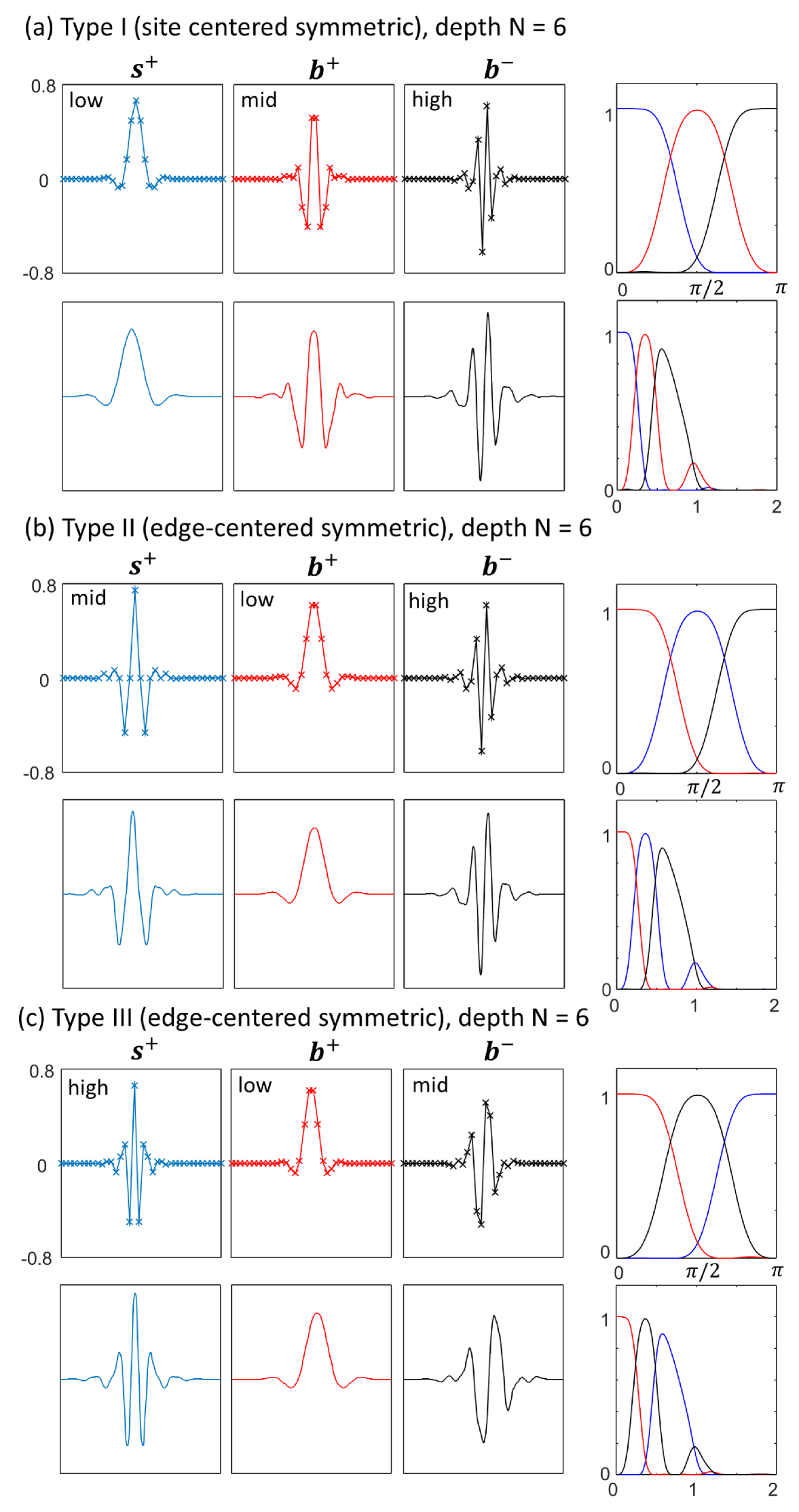
Choosing the angles that parameterize the ternary circuit to maximize the vanishing moments of the wavelets, as per Sect. IV.1.2, has several notable deficiencies. One of these deficiencies if that the symmetric and anti-symmetric wavelets seen in Fig. 7 are not well separated when resolved in frequency space; ideally we want the three-channel filter bank represented by circuit to possess well resolved low, mid, and high frequency components. A second deficiency is that the scaling functions in Fig. 7 still contain a significant high frequency component, which results in the corresponding wavelets not having a high degree of smoothness. In this Section we explore an alternative optimization criteria that resolves these deficiencies.
The alternative criteria we propose is that the circuit should be optimized such that some sequences have vanishing moments at high frequencies,
| (98) |
A three-channel wavelet filter bank with well resolved low/mid/high frequencies can be achieved by requiring that the scaling function and one of the wavelets satisfy the (high frequency) orthogonality constraint of Eq. 98 for some (while also requiring that both wavelets satisfy the standard vanishing moment criteria of Eq. 14). Recall that the ternary unitary circuit has three associated sequences , as such there freedom as to how the sequences are associated to the low/mid/high frequency components (which also informs whether the bond-centered or edge-centered form of the ternary circuit is used, see Fig. 6). Specifically, there are three choices (which we call Types I-III) that are compatible with the symmetries of the sequences, see Tab. 5.
In Tab. 6 we present angles for ternary circuits of depth for each of the wavelet types I-III, which were again optimized numerically using Nelder-Mead minimization. The wavelet sequences were optimized to satisfy the (low frequency) orthogonality constraint of Eq. 14 for , while the scaling and mid-frequency wavelet sequences were simultaneously optimized to satisfy the (high frequency) orthogonality constraint of Eq. 98 for . Interesting to note is that the Type II wavelet has and , which can be shown to imply that the sequence is strictly zero for all even indexed entries, i.e. for even , which is compatible with its status as the mid-frequency wavelet. Furthermore, the final layer of gates could also be omitted, such that it could be regarded as a depth ternary circuit that has an extra layer of swap gates on the bottom. Notice that the deficiencies observed in the previous class of scale factor 3 wavelets, Fig. 7, have been resolved; the new wavelets have high smoothness and are well separated into low/mid/high frequency components.
| Type I | Type II | Type III | |
|---|---|---|---|
| 0.072130476 | -0.261582176 | 0.072130476 | |
| 0.847695078 | -0.847695078 | ||
| -0.576099009 | 0.107465734 | -0.576099009 | |
| -0.591746629 | 0.591746629 | ||
| 0.673886987 | -0.461363266 | 0.673886987 | |
| 0.529449713 | 0 | -0.529449713 |
IV.2 Dilation symmetric multi-wavelet transform
An alternative solution to form symmetric orthogonal wavelets, other than from increasing the dilation factor , is to use multiwavelets, which possess more than one distinct scaling function (see for instance Refs. Multi1, ; Multi2, ; Multi3, ; Multi4, ). In this section we use the unitary circuit formalism to construct a family of dilation factor 2 multi-wavelets (noting that analogous constructions have previously been considered in the context of the MERAMERAbook ) where the two distinct scaling functions are each exactly reflection symmetric, and the two distinct wavelet functions are reflections of one another.
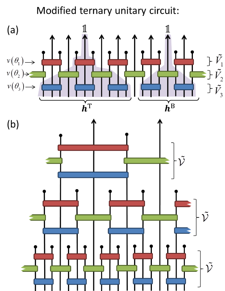
IV.2.1 Modified ternary unitary circuits
Let be a matrix; we say that is a depth modified ternary circuit if it can be decomposed as a product of layers,
| (99) |
see also Fig. 9(a), where each layer is composed of a direct sum of reflection symmetric unitary matrices , as defined in Eq. 90, that are spaced by single site identities ,
| (100) |
Additionally we require that each layer is offset by sites from the proceeding layer. Notice that the depth modified ternary circuit is parameterized by the set of angles .
The modified ternary circuit , which invariant under translations by four sites, may be interpreted as a four-channel filter bank. We label the four corresponding coefficient sequences , , and , each of which is given by transforming a unit vector, i.e. as . The sequences possesses the following properties,
-
•
is a site-centered symmetric sequence of (odd) length elements (i.e. that is symmetric w.r.t. reflections about the central element), and is given from transforming the unit vector located at the center of , see Fig. 9(a).
-
•
is a site-centered symmetric sequence of (odd) length elements (i.e. that is symmetric w.r.t. reflections about the central element), and is given from transforming the unit vector located at the center of , see Fig. 9(a).
-
•
and are length sequences given from transforming the unit vector located at the left and right index of respectively, and are related to each other by spatial reflection.
A multi-scale circuit can be formed by composition of modified ternary circuits, , where both and are treated as scaling sequences, see also Fig. 9(b), which in turn represents the multiwavelet transform of dilation factor .
| 0.161653803 | 0.190056742 | |
|---|---|---|
| 0.389671265 | 0.438258716 | |
| 0.395157917 | 0.389371447 | |
| 0.167734951 | -0.938456988 | |
| - | 0.319668509 | |
| - | 0.875926194 | |
| - | -1.048336048 | |
| - | 0.314028313 | |
| - | 0.843502411 |
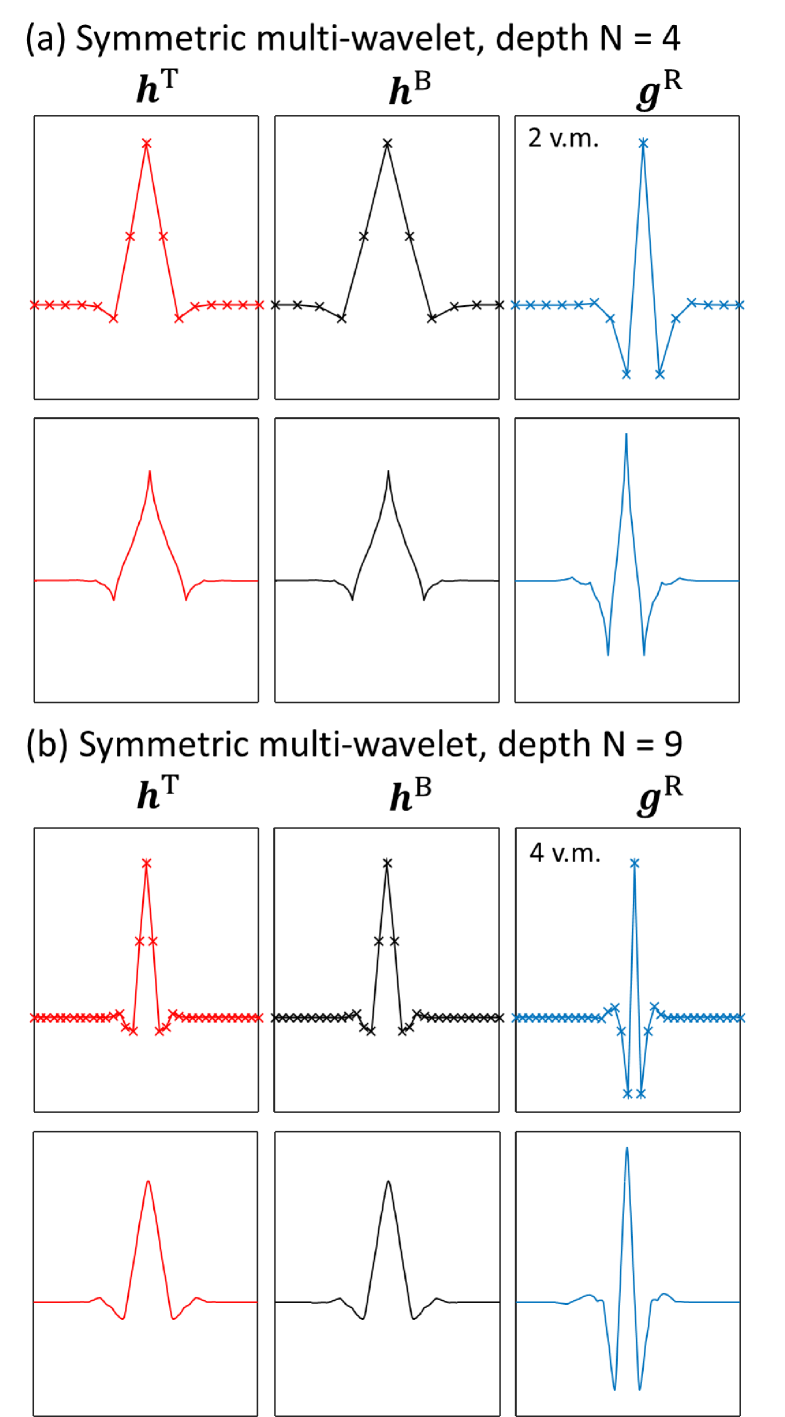
IV.2.2 Example 3: dilation symmetric multi-wavelets
There are many possible criteria for optimization of the angles associated to the depth modified ternary circuit . One choice could be to optimize to maximize the number of vanishing moments that the wavelets possess. For instance, if angles were chosen such that the wavelet sequences and possessed vanishing moments, see Eq. 14, for and the scaling sequences and had vanishing moments for , then the family of multi-wavelets given from composition of would possess vanishing moments. Using this criteria we have found solutions for circuits depth with vanishing moments, and for depth with vanishing moments, although we do not present these results here.
Instead, in Tab. 7 we present solutions for depth with vanishing moments, and for depth with vanishing moments. Here the extra degrees of freedom (resulting from use of larger depth circuits than is necessary to achieve the desired number of vanishing moments) have been used to minimize the difference between the two distinct scaling sequences and of the multiwavelet transform, which also imposes that the wavelet sequences and are each individually close to being reflection symmetric. This was achieved using the Nelder-Mead algorithm to numerically optimize the angles as to minimize the magnitude of the desired scaling and wavelet sequence moments, as usual, but where a small term was also included in the figure of merits that penalized the difference between the two distinct scaling sequences. The term used was of the form , where
| (101) |
and scalar was a small fixed parameter. Note that the sequence in Eq. 101 has been padded by two zero elements at the start and end of the sequence, such that the padded sequence is of the same length as .
The resulting wavelets are plotted in Fig. 10, which are seen to closely resemble the corresponding coiflets with and vanishing moments. In both examples only very small differences between the two scaling sequences are realized; for the depth example we have , while for the depth example we have . In comparison with coiflets, where the scaling functions are only approximately reflection symmetric, here we have achieved exact symmetry at the expense of now having two distinct (yet almost identical) scaling functions.
IV.3 Dilation symmetric wavelets
In this section we construct an example family of exactly reflection symmetric and antisymmetric wavelets of dilation factor using a unitary circuit formalism. The purpose of this example is to demonstrate an alternate construction of symmetric wavelets that is not based upon the individually symmetric unitary matrices as considered in Sects. IV.1 and IV.2. Instead, the circuit that represents the symmetric wavelet transform is built from unitary matrices.
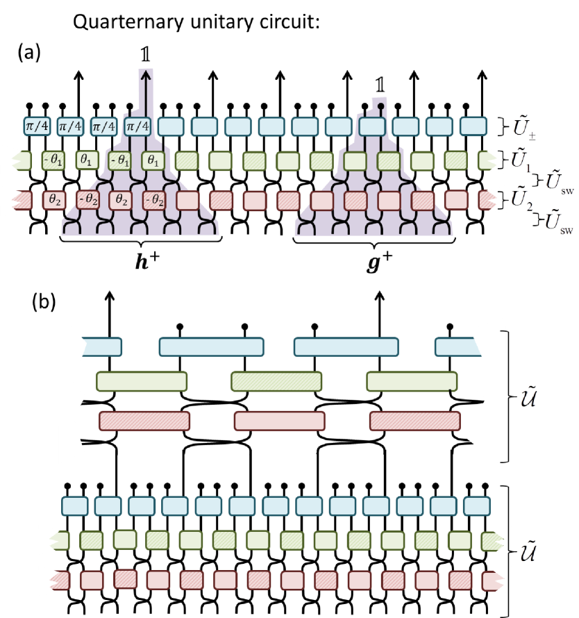
IV.3.1 Quaternary circuits
Let be a matrix for positive integer ; we say that is a depth quaternary unitary circuit if it can be decomposed into sublayers , each of which is a direct sum of unitary matrices ,
| (102) |
where unitaries are parameterized by a rotation angle , see Eq. 8, which alternates in sign with position, see also Fig. 11(a). Layers of the quaternary unitary circuit are inter-spaced with layers of swap gates,
| (103) |
with the two site swap gate as defined in Eq. 88, and the quaternary circuit also includes a top sublayer composed of unitary gates ,
| (104) |
Notice that the depth quaternary unitary circuit is parameterized by the set of angles .
The quaternary unitary circuit, which is invariant w.r.t translations of four sites, may be interpreted as a four-channel filter bank. The four corresponding coefficient sequences , each given from transforming the unit vector on a non-equivalent site, have the following properties:
-
•
is a edge-centered symmetric sequence of (even) length elements, given from transforming with .
-
•
is a edge-centered antisymmetric sequence of (even) length elements, given from transforming with .
-
•
is a edge-centered symmetric sequence of (even) length elements, given from transforming with .
-
•
is a edge-centered antisymmetric sequence of (even) length elements, given from transforming with .
The symmetry of the coefficient sequences can be understood by recalling that , where denotes spatial reflection, which implies that constitutes a unitary matrix that is reflection symmetric.
A multi-scale circuit, which represents a family of wavelet transform of dilation factor , is formed by composition of quaternary circuits, where is treated as the scaling sequence, see also Fig. 11(b).
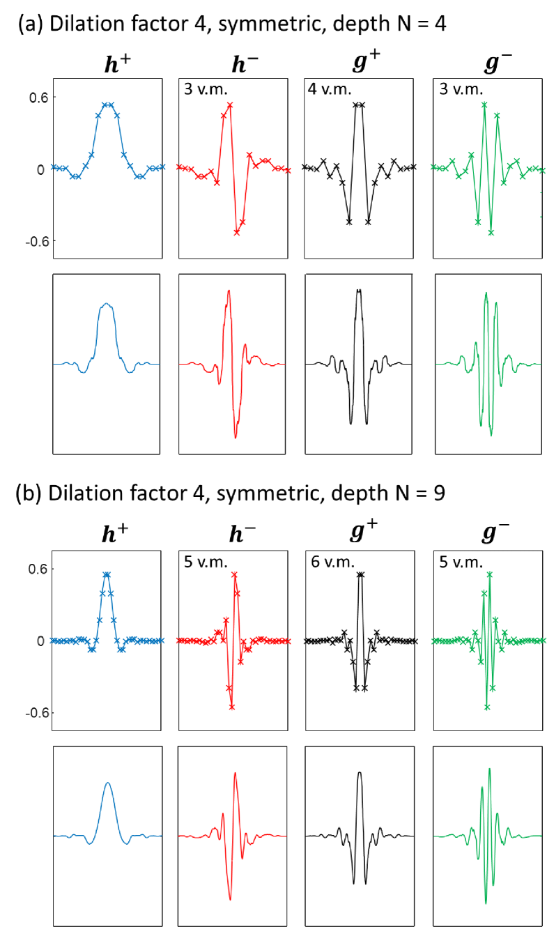
IV.3.2 Example 4: dilation symmetric wavelets
For a depth quaternary circuit, we optimize the free angles numerically using the Nelder-Mead algorithm to give wavelet sequences with as many vanishing moments as found to be possible. Two sets of example angles, one for depth and the other for depth , are given in Tab. 8. The depth circuit yields wavelets with vanishing moments for orders , while the depth circuit yields wavelets with vanishing moments for orders . These example wavelets, shown in Fig. 12, display a relatively high smoothness while also maintaining a small effective support, which suggests they may perform well in perform well in practical applications.
| -1.229229752 | 2.807164665 | |
|---|---|---|
| 0.102977579 | -0.473049662 | |
| 1.918752569 | -1.482553131 | |
| -0.198852925 | -1.922365069 | |
| - | -3.091128284 | |
| - | 2.257247480 | |
| - | 2.554082219 | |
| - | -0.492838196 | |
| - | -0.633172753 |
IV.4 Boundary wavelets
In this section we explore the use of unitary circuits in the construction of boundary waveletsBound1 ; Bound2 ; Bound3 ; Bound4 , using a similar approach to the boundary MERA developed in the context of studying quantum spin chains with open boundariesBoundMERA1 ; BoundMERA2 .
| 0.615479708 | 0.261157410 | |
| 0.713724378 | 0.316335000 | |
| 0.752040089 | 0.339836909 | |
| 0.769266332 | 0.350823961 | |
| 0.777461322 | 0.356148400 | |
| 0.781461114 | 0.358770670 | |
| 0.783437374 | 0.360072087 | |
| 0.784419689 | 0.360720398 | |
| 0.784909404 | 0.361043958 | |
| 0.785153903 | 0.361205590 | |
| 0.785276063 | 0.361286369 | |
| 0.785337120 | 0.361326749 |
IV.4.1 Example 5: boundary wavelets for D4 Daubechies wavelets
Here we provide an example the use of a unitary circuit in the construction of boundary wavelets for the specific case of the D4 Daubechies wavelets, although the general strategy we employ for constructing the boundary wavelets can easily be extended not only to higher order Daubechies wavelets, but also to other wavelet families. The boundary wavelets we construct are orthogonal and, as with the D4 Daubechies wavelets, possess two vanishing moments.
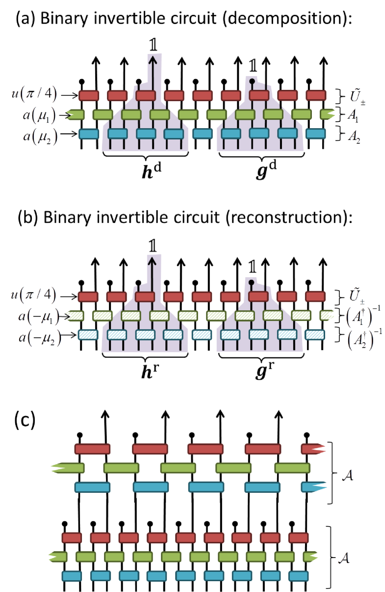
The boundary wavelets are parameterized using a boundary unitary circuit, see Fig. 13, which is constructed as follows. Let be a semi-infinite lattice of sites , i.e. with an open boundary on the left. We apply as much of the multi-scale circuit corresponding to the D4 wavelets, i.e. composed of depth binary unitary circuits with angles and (see Sect. III.2), that can be supported on . Then a double layer of scale-dependent unitary gates, parameterized by angles and , where subscripts here denote scale , is introduced on the boundary of the multi-scale circuit.
Starting from the lowest scale the angles and are fixed such that the corresponding boundary wavelet at that scale, as depicted in Fig. 13(a), has two vanishing moments. Here the angles and can be found deterministically using a algorithm similar to the circuit construction algorithm discussed in Sect. III.3.2. We then apply the algorithm iteratively, scale-by-scale, to fix remaining angles and such that all boundary wavelets have two vanishing moments. The resulting angles are given in Tab. 9, and are seen to converge to the values and in the large scale limit, .
The resulting boundary wavelets are plotted in Fig. 14 over several different scales . Notice that the double layer of unitary gates was used in the boundary circuit of Fig. 14 in order to provide two degrees of freedom and for each boundary wavelet (which could then be chosen in order to endow each boundary wavelet with two vanishing moments). More generally additional layers of boundary unitary gates could be included in order to generate wavelets with higher vanishing moments.
IV.5 Biorthogonal wavelets
Biorthogonal wavelets, such as the CDF wavelets introduced in Ref. Daub3, , follow from removing the orthogonality constraint on wavelets while still requiring perfect reconstruction. For a given number of vanishing moments, biorthogonal wavelets can possess smaller support than orthogonal wavelets, and can be exactly symmetric even for dilation factor . These properties make biorthogonal wavelets useful in practical applications such as image compression, where they are employed in the JPEG2000 format JPEG .
In this section we briefly discuss the use of a circuit formalism in the construction of biorthogonal wavelets. First we introduce the notion of invertible circuits which are built from many copies of local invertible matrices, and follow from relaxing the unitary constraint on the circuit formalism. As with the case of the unitary circuits explored in this manuscript, many different forms of invertible circuit could be considered; here the example we provide leads to a novel family of (edge-centered) antisymmetric biorthogonal wavelets.
IV.5.1 Binary invertible circuits
We consider a circuit with the same structure as the binary unitary circuits considered in Sect. II, but where the unitary constraint on the matrices has been removed, and instead the matrices are constrained to be reflection symmetric. Let be a reflection symmetric matrix parameterized by real parameter ,
| (105) |
and let be an invertible matrix of dimension for integer . We say that is a binary invertible circuit of depth if it can be decomposed into sublayers,
| (106) |
see also Fig. 15(a), where is a direct sum of unitary gates as defined in Eq. 104. Here is a matrix given as the direct sum of matrices ,
| (107) |
and each sublayer is offset by one site from the preceding sublayer. Notice that the depth circuit is parameterized by the real numbers restricted such that .
We wish to interpret the binary invertible circuit as the decomposition part of a two-channel filter bank. Let be a vector of length , which we transform to new vector using the binary invertible circuit ,
| (108) |
The original vector can be reconstructed from as,
| (109) |
where , which we refer to as the dual of , is the corresponding reconstruction part of a two-channel filter bank.
Let us now examine the form of the dual circuit. The inverse-transpose can be taken of each sublayer individually,
| (110) |
where again each sublayer is offset by one site from the preceding sublayer, see also Fig .15(b). Notice that the transpose of it is own inverse. Similarly, since it can be shown that (for ),
| (113) | ||||
| (114) |
it follows that is a given as the direct sum of matrices ,
| (115) |
We label the (decomposition) scaling and wavelet sequences as and respectively, which are given from , and the (reconstruction) scaling and wavelet sequences as and respectively, which are given from , see also Fig. 15(a-b). These coefficient sequences have the following properties:
-
•
and are a edge-centered symmetric sequences of (even) length elements.
-
•
and are a edge-centered antisymmetric sequences of (even) length elements.
Once again the binary invertible circuit can be composed to form a multi-scale circuit,
| (116) |
see also Fig .15(c), which encodes a family of antisymmetric biorthogonal wavelets of dilation factor .
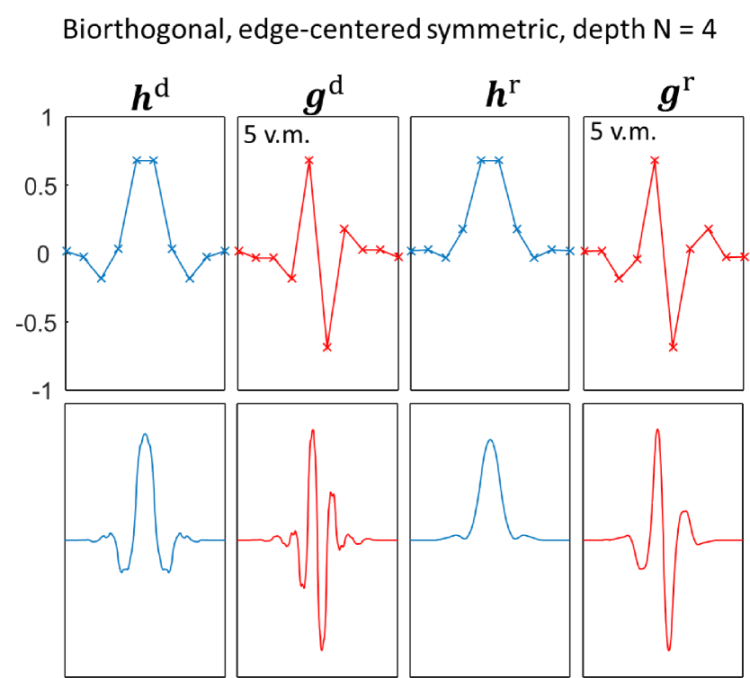
IV.5.2 Example 6: edge-centered symmetric biorthogonal wavelets
Here we provide an example of biorthogonal wavelets constructed using a binary invertible circuit. For a depth binary invertible circuit we use algebraic methods to fix the parameters , see Tab. 10, such that both the decomposition and reconstruction wavelets have vanishing moments for . The resulting antisymmetric wavelets are depicted in Fig. 16.
| -0.25684952118 | |
| 0.85058116979 | |
| 0.05040158211 | |
| -0.83314630482 |
V Conclusions
The main objectives of this manuscript were to recast wavelets in the circuit formalism familiar to multi-scale methods used for simulating quantum many-body systems, thereby further elaborating on the connections between these fields, and also to explore the use of the circuit formalism in the design of novel wavelet transforms.
The representation of common orthogonal wavelet families, such as Daubechies wavelets, symlets and coiflets, as unitary circuits composed of rotation matrices, which are parameterized by rotation angles , appears to be a very natural one. The circuit representation makes explicit key properties of the wavelets (such as orthogonality), facilitates in the understanding of aspects of their construction (such as the cascade algorithm), and is amenable to their efficient numeric implementation. Furthermore, as evidenced in Tabs. 1, 2 and 3 and Fig. 4, parameterization in terms of rotation angles affirms a clear-cut relation between different orders of wavelets within the same family.
The families of wavelets given in Sect. IV were constructed via a two-step process that involved (i) the design of the circuit that builds desired properties into the parameterization (e.g. orthogonality, symmetry, dilation factor) and (ii) numerical optimization of the parameters according to some specified criteria (e.g. to achieve the maximal number of vanishing moments). Interestingly, these are the same two steps involved in the implementation of MERA for the study of quantum many-body systems, where the criteria for the numerical optimization in (ii) then involves minimizing the energy of the MERA with respect to a system Hamiltonian. In most of the examples presented in this manuscript the Nelder-Mead algorithm, a standard numeric algorithm for minimizing a multi-dimensional objective function, was used in the optimization of the circuit parameters, although more sophisticated numerical or analytic methods could, in general, also be employed.
The examples provided were intended to demonstrate the utility of the circuit formalism in wavelet design, but certainly do not constitute an exhaustive list of the wavelets that can be constructed using this approach. For each of the circuit examples provided, one could straight-forwardly consider higher order wavelets based on larger depth circuits, as well as alternative optimization criteria for the free parameters of the circuits. Many other circuit designs are also possible, including circuits in higher dimensions, analogous to higher dimensional implementations of MERAAlg2 ; MERAapp4 , which could represent novel families of non-separable orthogonal (or ) wavelets. Despite only intending to serve as examples, many of the wavelets given appear to perform well in practical applications. Though not presented in this manuscript, preliminary investigations suggest that the wavelets described in examples 2, 3 and 6 perform similarly to, or in some cases exceed the performance of, the CDF-9/7 wavelets in application to image compression. The use of circuits in optimal wavelet design for specific applications remains an interesting direction for future research.
The authors acknowledge support by the Simons Foundation (Many Electron Collaboration). SRW acknowledges funding from the NSF under grant DMR-1505406.
References
- (1) M. T. Fishman and S. R. White, Compression of Correlation Matrices and an Efficient Method for Forming Matrix Product States of Fermionic Gaussian States, Phys. Rev. B 92, 075132 (2015).
- (2) G. Evenbly and S. R. White, Entanglement renormalization and wavelets, Phys. Rev. Lett. 116, 140403 (2016).
- (3) I. Daubechies, Orthonormal bases of compactly supported wavelets, Comm. Pure Appl. Math. 41 (1988) 909-996.
- (4) I. Daubechies, Ten Lectures on Wavelets, in: CBMS Conf. Series in Appl. Math., Vol. 61, SIAM, Philadelphia, 1992.
- (5) A. Cohen, I. Daubechies, and J. C. Feauveau, Biorthogonal bases of compactly supported wavelets, Comm. Pure Appl. Math., 1992, 45, 485-500.
- (6) I. Daubechies, Orthonormal bases of compactly supported wavelets II Variations on a theme, SIAM J. Math. Anal., 1993, 24, 499-519.
- (7) P. P. Vaidyanathan, Multirate Systems and Filter Banks, Prentice Hall, ISBN-10: 0136057187 (1993).
- (8) C.S. Burrus, R.A. Gopinath, and H. Guo, Introduction to Wavelets and Wavelet Transforms: A Primer, Prentice-Hall, ISBN 0-13-489600-9 (1998).
- (9) F. Keinert, Wavelets and multiwavelets, CRC Press, ISBN 1-58488-304-9 (2003).
- (10) J. Shapiro, Embedded image coding using zerotrees of wavelet coefficients, IEEE Trans. Signal Processing, vol. 41, pp. 3445-3462, Dec. 1993,
- (11) S. Mallat, A Wavelet Tour of Signal Processing, Boston, MA: Academic, ISBN-13: 978-0123743701 (1998).
- (12) A. Skodras, C. Christopoulos, and T. Ebrahimi, The JPEG2000 still image compression standard, IEEE Signal Processing Mag., vol. 18, pp. 36-58, Sept. 2001.
- (13) For a review of the renormalization group see: M.E. Fisher, Renormalization group theory: its basis and formulation in statistical physics, Rev. Mod. Phys. 70, 653 (1998).
- (14) G. Vidal, Entanglement renormalization, Phys. Rev. Lett. 99, 220405 (2007).
- (15) G. Vidal, A class of quantum many-body states that can be efficiently simulated, Phys. Rev. Lett. 101, 110501 (2008).
- (16) R.N.C. Pfeifer, G. Evenbly, and G. Vidal, Entanglement renormalization, scale invariance, and quantum criticality, Phys. Rev. A, 79, 040301(R) (2009).
- (17) G. Evenbly, P. Corboz, and G. Vidal, Non-local scaling operators with entanglement renormalization, Phys. Rev. B 82, 132411 (2010).
- (18) G. Evenbly and G. Vidal, Quantum criticality with the multi-scale entanglement renormalization ansatz, in: “Strongly Correlated Systems: Numerical Methods”, edited by A. Avella and F. Mancini (Springer Series in Solid-State Sciences, Vol. 176 2013).
- (19) G. Evenbly and G. Vidal, Entanglement renormalization in two spatial dimensions, Phys. Rev. Lett. 102, 180406 (2009).
- (20) Y.-L. Lo, Y.-D. Hsieh, C.-Y. Hou, P. Chen, and Y.-J. Kao, Quantum Impurity in Luttinger Liquid: Universal Conductance with Entanglement Renormalization, Phys. Rev. B 90, 235124 (2014).
- (21) G. Evenbly and G. Vidal, Algorithms for entanglement renormalization: boundaries, impurities and interfaces, J. Stat. Phys. 157:931-978 (2014).
- (22) J. C. Bridgeman, A. O’Brien, S. D. Bartlett, and A. C. Doherty, MERA for Spin Chains with Continuously Varying Criticality, Phys. Rev. B 91, 165129 (2015).
- (23) G. Evenbly and G. Vidal, Frustrated antiferromagnets with entanglement renormalization: ground state of the spin-1/2 Heisenberg model on a kagome lattice, Phys. Rev. Lett. 104, 187203 (2010).
- (24) For an overview of the early connections between wavelets and RG see: G. Battle, Wavelets: A renormalization group point of view, in “Wavelets and Their Applications”, edited by M. B. Ruskai (Bartlett and Jones, 1992). G. Battle, Wavelets and Renormalization, World Scientific, ISBN-13: 978-9810226244 (1999).
- (25) G. Evenbly and G. Vidal, Algorithms for entanglement renormalization, Phys. Rev. B, 79, 144108 (2009).
- (26) G. Evenbly, R. N. C. Pfeifer, V. Pico, S. Iblisdir, L. Tagliacozzo, I. P. McCulloch, and G. Vidal, Boundary quantum critical phenomena with entanglement renormalization, Phys. Rev. B 82, 161107(R) (2010).
- (27) P. Silvi, V. Giovannetti, P. Calabrese, G. E. Santoro, and R. Fazio, Entanglement renormalization and boundary critical phenomena, J. Stat. Mech. L03001 (2010).
- (28) C. Chui and J. Lian, Construction of compactly supported symmetric and antisymmetric orthonormal wavelets with scale=3, Appl. Comput. Harmon. Anal., 2, 21–51 (1995).
- (29) A. Petukhov, Construction of symmetric orthogonal bases of wavelets and tight wavelet frames with integer dilation factor, Appl. Comput. Harmon. Anal., 17, 198–210 (2004).
- (30) B. Han, Symmetric orthogonal filters and wavelets with linear-phase moments, J. Comp. Appl. Math., 236, 482–503 (2011).
- (31) A. Krivoshein and M. Ogneva, Symmetric orthogonal wavelets with dilation factor M = 3, Journal Of Mathematical Sciences, November 8, 2013;194(6):667-677.
- (32) C. K. Chui and J. Lian, A study on orthogonal multiwavelets, J. Appl. Numer. Math. 20, 273–298 (1996).
- (33) Q. T. Jiang, Symmetric paraunitary matrix extension and parametrization of symmetric orthogonal multifilter banks, SIAM J. Matrix Anal. Appl. 23(1), 167–186 (2001).
- (34) R. Turcajová, An algorithm for the construction of symmetric orthogonal multiwavelets, SIAM J. Matrix Anal. Appl. 25(2), 532–550 (2003).
- (35) X. X. Feng, Z. P. Yang, and Z. X. Cheng, The Parameterization of 2-Charmel Orthogonal Multifilter Banks with Some Symmetry, J. Appl. Math. & Computing, 26: 151-168 (2008).
- (36) C. Chui and E. Quak, Wavelets on a bounded interval, in “Numerical Methods of Approximation Theory”, edited by D. Braess and L. L. Schumaker, pages 1-24. Birkhäuser-Verlag, Basel (1992).
- (37) A. Cohen, I. Daubechies, and P. Vial, Wavelets on the interval and fast wavelet transforms, Appl. Comput. Harmon. Anal., 1 (1993), pp. 54–81.
- (38) L. Andersson, N. Hall, B. Jawerth, and G. Peters, Wavelets on closed subsets of the real line, Recent Advances in Wavelet Analysis, Wavelet Anal. Appl., vol. 3, Academic Press, Boston, MA (1994), pp. 1–61.
- (39) W.R. Madych, Finite orthogonal transforms and multiresolution analyses on intervals, J. Fourier Anal. Appl., 3 (1997), pp. 257–294.