Seed Layer Engineering for Crack-free Sol-gel Alumina Deposition on GFETs
Abstract
Low cost and low thermal budget based spin-coated sol-gel Alumina was explored as a dielectric/passivation layer for GFET. Post thermal annealing, the crack was observed in sol-gel Alumina layer exactly above the graphene channel. The possible mechanism of crack could be graphene lateral restoring movement due to (i) Thermal Expansion Coefficient (TEC) difference between graphene and adjacent layers and (ii) shrinkage stress generated during the solvent removal process. Based on the crack formation phenomenon, a combination of different annealing schemes (low thermal budget DUV annealing) and seed layer engineering (thickness and different deposition schemes) were carried out. Finally, a novel two-step seed layer deposition method with DUV annealing was proposed and demonstrated to resolve the crack issue successfully and also able to retain the Dirac point in the electrical characteristics.
Index Terms:
Monolayer graphene, GFET, sol-gel, Seed layer engineering, Dirac point, DUV annealingI Introduction
The uniqueness in the properties of graphene like am-bipolar transport, high carrier mobility [1], exceptional mechanical strength [2], thermal properties [3] and flexible nature [4] have paved the way for the RF applications over conventional materials [5]. Dielectric materials plays an important role of gate dielectric and passivation layer for any FET devices. There are different techniques like PVD [6, 7] and ALD [8, 9, 10, 11] to deposit high quality dielectric layers. On the other hand there are reports of solution based deposition techniques through spin or spray coatings for dielectric materials [12]. These techniques have advantages of high deposition rate, no vacuum requirement, low cost method, tuning of the precursor composition [13] and can be used for flexible applications [14]. But there are also several challenges in using solution based deposition techniques like (i) adhesion of spray or spin coated layer with the underneath layer and (ii) need to anneal layers post deposition to remove solvent from the layer, which leads to stress in the films.
The most commonly used dielectrics for the GFETs are Si3N4 [15], HfO2 [16] and Al2O3 [17]. Among them, the Al2O3 has proven to be the best passivation layer due to its high thermal stability, appreciable permeability barrier and reduced hysteresis in transfer characteristics in FET devices [18]. The presence of the Al2O3 monolayer does not introduce interface states and electron-hole puddles in graphene [19]. Recently the sol-gel Alumina (Al2O3) has been extensively used in the solar cells as a field-effect passivation layer [20] due to its good interface quality and dielectric breakdown. Park et.al[21, 22] and Bae et.al[23] have explored sol-gel Alumina on the graphene transistors as dielectric layer and pH sensing membrane.
Before sol-gel Alumina spin coating, the surface of graphene needs to be made hydrophilic for its proper adhesion. There are few techniques like plasma exposure [24], functionalisation [25], seed layer deposition [21, 26] explored for wetting the graphene surface. Techniques such as O2 plasma exposure, UV-O3 irradiation and functionalization would create lattice damage [27] and doping to the graphene[25]. On the other hand, the seed layer deposition does not create any lattice damage and also won’t create any P-type doping [10, 28, 29]. The deposition of the seed layer is usually carried out by the e-beam evaporation technique as it provides structural and morphological control of films and offers low resistivity [30]. The e-beam lacks uniform deposition in the inner surface of 3D complex geometries due to the shadowing effect caused by line of sight deposition [31]. Sputtering can also be used as an alternative for deposition of a seed layer for conformal coverage of steps and trenches [32]. The problem associated with sputtering was that it can damage the underlying surface with plasma.
The proper densification of sol-gel thin film requires an annealing process to remove the solvent and also some trapped byproducts from the oxide network [23, 21]. The conventional method i.e thermal annealing mostly requires elevated temperature which can cause strain [33] and unintentional doping [34] in graphene devices. Also, during the annealing of the sol-gel solution, the drying stress due to the differential shrinkage (capillary forces) of the gel will be present [13, 35]. But at high temperatures, the films are prone to undergo in-plane stress i.e tensile stress during the heating and compressive stress after cooling [36, 37]. To reduce annealing temperature, techniques such as Deep Ultra Violet (DUV) annealing [38, 39, 40], O3 annealing [41], Microwave annealing [26, 42, 22, 43], High pressure annealing [44] are mostly used. Among these DUV annealing process was the most explored and readily available technique for sol-gel Alumina [39].
In this work, we report fabrication of sol-gel alumina based GFET devices. We discovered crack formation in the sol-gel Alumina layer post annealing. We explored seed layer engineering and different annealing techniques (Thermal and DUV) based on understanding different phenomenons to resolve the crack issue. Finally we propose novel two step method to resolve the crack issue.
II Experimental
II-A Synthesis of sol-gel Alumina
The synthesis of sol-gel Alumina was carried out by mixing the Aluminum nitrate nonahydrate (Al(NO3)3.9H2O) (from Sigma Aldrich) with CMOS grade Isopropyl alcohol (C3H7OH). The mixture was stirred for 12 hours and the resultant solution was filtered using a membrane filter with a pore size of 0.22 m. The molarity of the resultant solution was kept at 0.1 M. The resultant solution was spin-coated on samples at 5000 rpm for 45 seconds. Thermal [21] and DUV annealing [39] techniques have been used to remove solvent from spin-coated sol-gel Alumina.
II-B Fabrication of GFETs
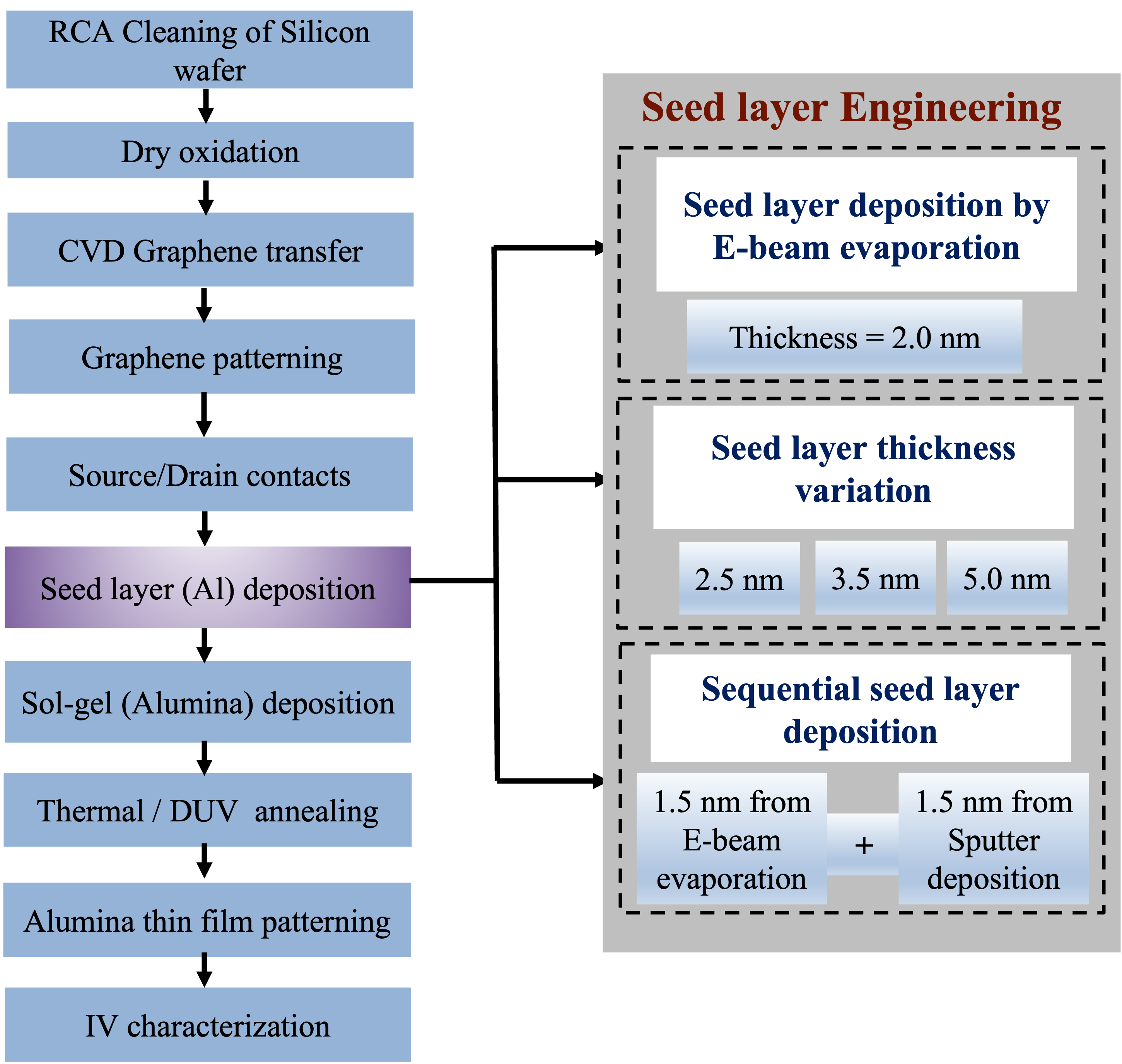
The fabrication flow of graphene-based transistor with a seed layer and passivation layer is shown in Figure 1. To fabricate the graphene transistors, CVD-grown graphene monolayer on copper foil were purchased from Graphenea Inc. These copper foil was cut into pieces and coated with 2 PMMA 950K. Next, the pieces were immersed in the Copper etchant solution. The isolated graphene layers were carefully transferred to a thermally oxidized 2-inch silicon substrate with a resistivity of 0.002-0.005 ohm-cm. The thickness of the SiO2 was kept at 90 nm to make the transferred graphene layer optically visible [45]. The backside oxide was etched using 7:1 buffered Hydrofluoric (BHF) acid solution for the substrate contact. Then, a graphene monolayer was patterned for the graphene channels using the optical lithography followed by the oxygen plasma exposure. The device dimensions used are width (W = 5-7m) and length (L = 20-30m). After channel definition, the source and drain contacts were made by using the electron beam evaporation (e-beam) of 10 nm Nickel and 40 nm Gold followed by the lift-off process. Thereafter, the Aluminum seed layer engineering was carried out as shown in Figure 1. Subsequently, the deposited seed layers were subjected to natural oxidation in the ambient atmosphere for one day. Next, the synthesized sol-gel Alumina was spin-coated followed by the thermal/DUV annealing. Finally, the densified sol-gel Alumina film was patterned to complete the device fabrication. The electrical characterization on the respective samples ware carried out done using a Keysight B1500A semiconductor device analyzer.
III Results and discussion
III-A Thin seed layer deposition by e-beam evaporation
Figure 2 shows the effect of thermal annealing on GFET with a seed layer thickness of 2 nm deposited using e-beam evaporation. The annealing was carried out on a hotplate at 250oC for 2 hours. During the densification by thermal annealing, the crack was observed in the sol-gel Alumina layer of GFET exactly above the graphene channel layer as shown in Figure 2 (a) and (b). The Atomic Force Microscopy (AFM) image (Figure 2 (c)) with profiling (Figure 2 (d)) conforms that crack formation in the sol-gel Alumina layer. The depth profile shows a non-uniformity at the edges of the cracks due to the agglomeration of the Alumina film after densification.
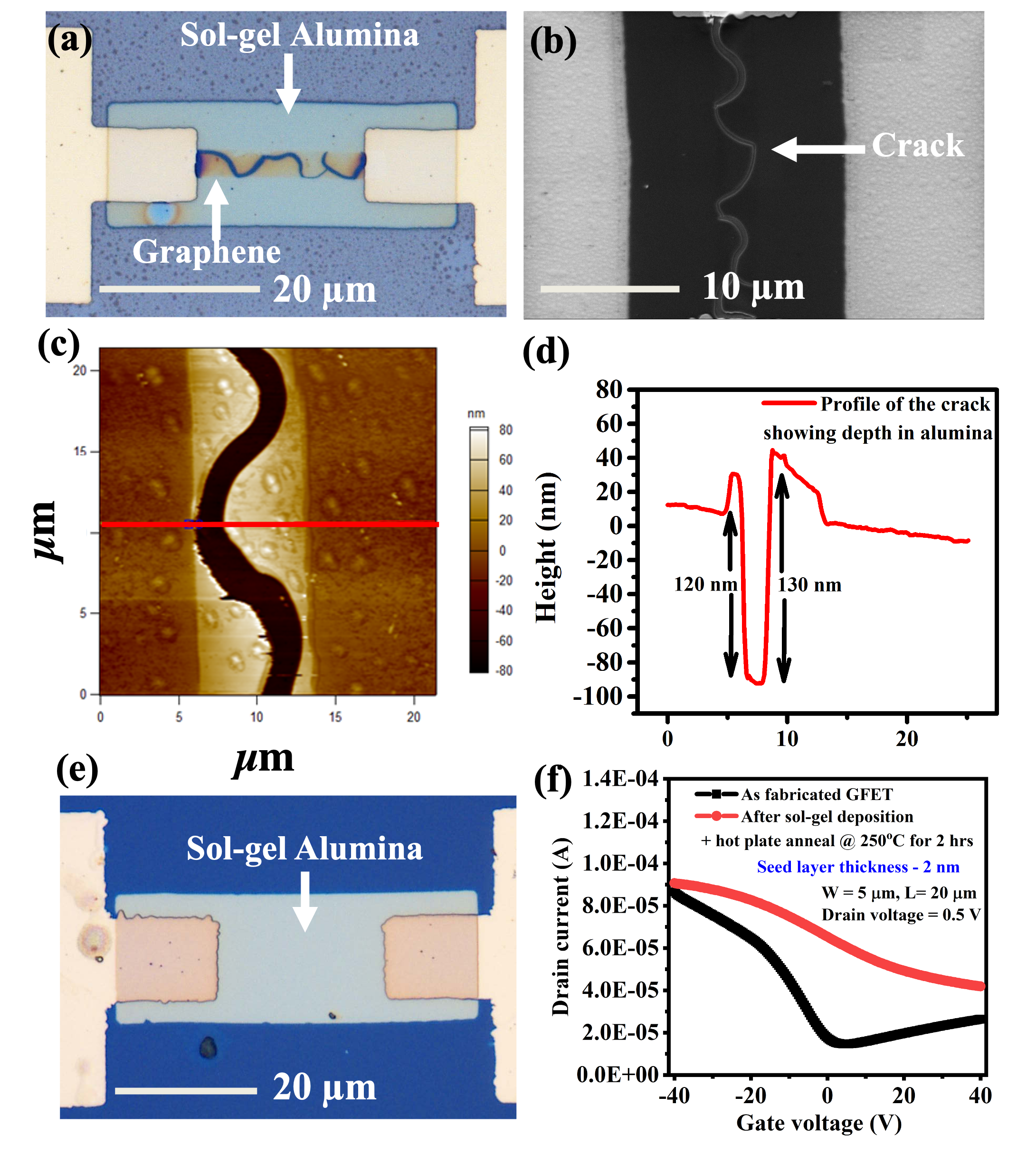
The origin of crack formation was investigated by fabricating the entire device without a graphene layer. It was found that there was no crack formation without a graphene layer (Figure 2(e)). This confirms that the graphene layer plays a major role in crack formation in the sol-gel Alumina layer during the annealing process. There could be the following two phenomenons happening during annealing, (i) solvent removal and (ii) expansion and/or compression of material depending upon the TEC of the material. There are reports of stress generated due to shrinkage of sol-gel Alumina during annealing [46, 13]. Positive TEC leads to expansion of material and negative annealing leads to compression during annealing. Graphene has a negative TEC [47], on other hand SiO2 substrate and oxidized seed layer has positive TEC [48, 49]. There are reports that when there was a negative TEC graphene on positive TEC SiO2 substrate, then it leads to slippage (lateral restoring movement) of graphene during annealing due to TEC difference between them [47]. The threshold temperature to cause slippage was reported to be 117oC [50]. Both of the above phenomena might lead to the movement of graphene, as graphene was residing on the substrate with van der Waals forces. The movement of graphene might lead to crack formation in the sol-gel Alumina film.
The Figure 2 (f) shows the transfer characteristics of GFET for device Figure 2(a). The output drain current after the thermal annealing of sol-gel Alumina shows the disappearance of the Dirac point and the electron branch. This conforms to the P-type nature of the graphene [51]. This is due to the diffusion of O2 and H2O from the ambient atmosphere which will form the redox reaction with the graphene during annealing [11] in addition to the stress. These redox reactions will form the OH-ions at the interface which will act as coulomb scatters.
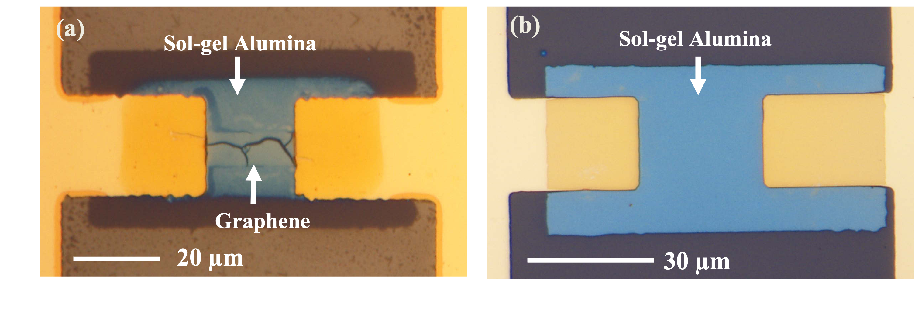
The TEC component can be reduced by using an annealing technique with a lower thermal budget. There are reports of DUV annealing to reduce thermal budget during annealing [39]. The DUV annealing technique has been applied in this work. The temperature was measured during DUV annealing using thermo-couple and it was found to be close to 70oC. The graphene device fabricated using DUV annealing still exhibits crack formation in the sol-gel layer exactly above the graphene layer as shown in the Figure 3(a). On the other hand, the device without graphene exhibits no crack as shown in the Figure 3(b). Hence it can be concluded that reducing the thermal budget was not sufficient to avoid crack formation. It means that even with DUV annealing the movement of graphene was not restricted.
III-B Seed layer thickness variation
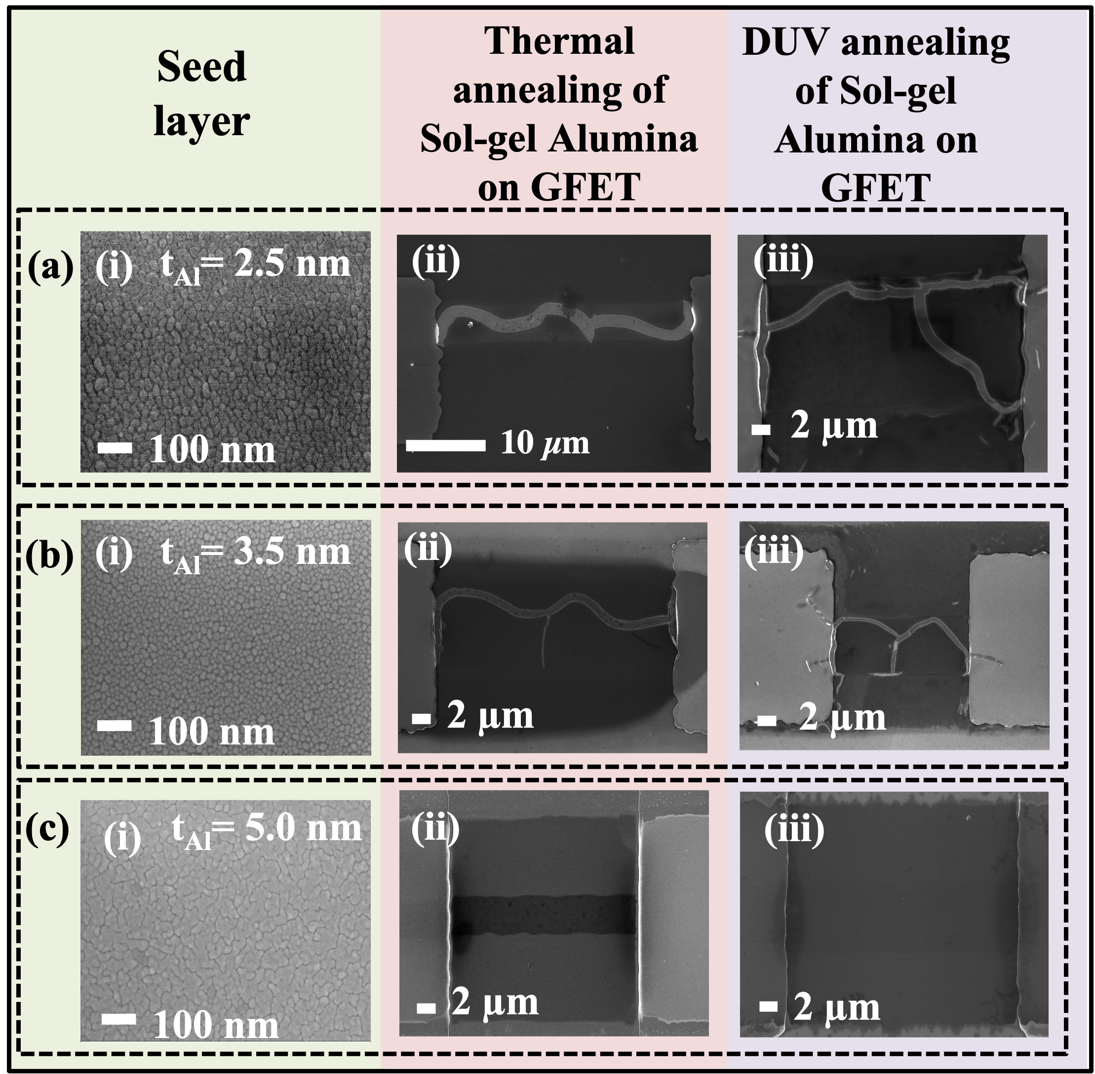
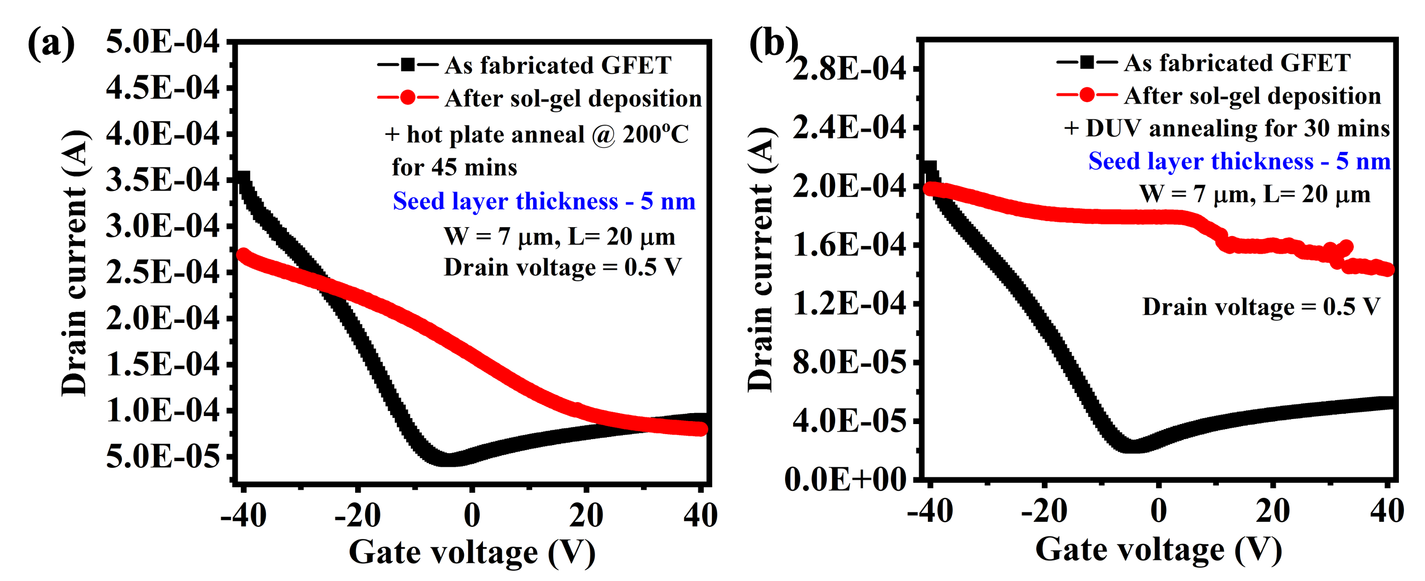
To further reduce graphene movement, different thicknesses (2.5, 3.5, and 5 nm) of seed layers were tried to make a graphene device. As shown in subfigures (i)-(iii) of Figure 4(a) and (b), it can be seen that graphene devices with 2.5 and 3.5 nm exhibit crack formation. On the other hand, 5 nm device does not show any crack formation as shown in Figure 4(c)(i)-(iii). Hence devices with thicker seed layers were able to restrict graphene movement to avoid crack formation. But when the graphene devices with a 5 nm seed layer were electrically tested before and after the sol-gel deposition as shown in the Figure 5(a) and (b). It was found that post-sol-gel deposition, devices show the disappearance of the Dirac point and resulted in the hole doping after the thermal annealing. In contrast, the drain current after DUV annealing did not show any modulation with gate voltage variation which means that the Aluminum seed layer could not have fully oxidized. Further deeper analysis of fabrication pointed out that a thin seed layer ( 2.5 nm) was deposited using e-beam evaporation, which was the line of sight deposition and might not lead to side-wall coverage (Figure 6(a)).
III-C Sequential seed layer deposition
To avoid insufficient oxidation and crack formation issues, we propose a novel two-step seed layer deposition approach. (i) first thin seed layer deposition using e-beam evaporation to avoid damage to graphene and (ii) thin seed layer deposition using sputter process to have sidewall coverage. The device was fabricated with a two-step process as shown in Figure 6(b)
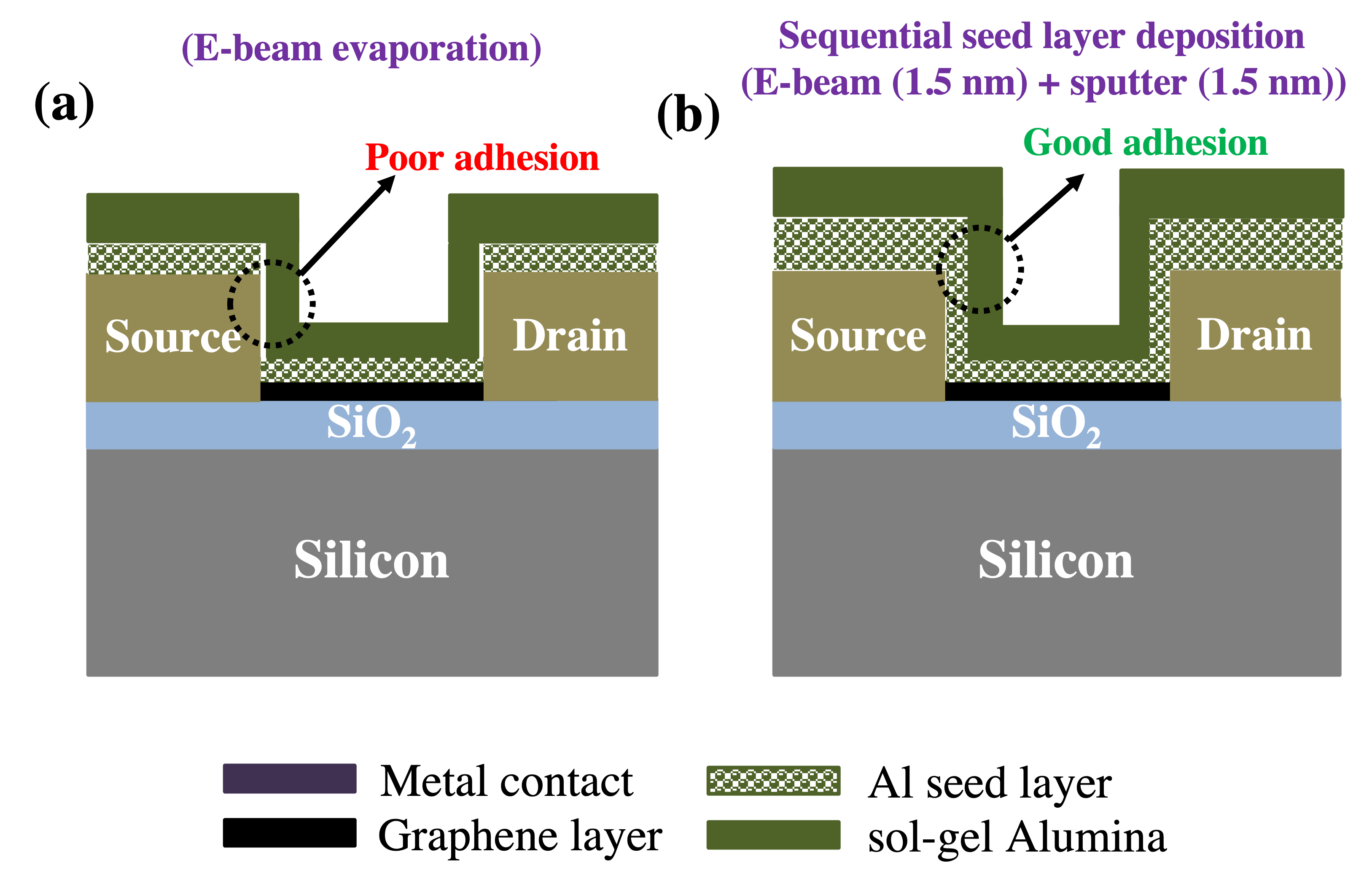
As shown in the Figure 7 (a) and (b), no cracks were observed in Alumina film on the graphene channel region. The sequential deposition will provide dense, hydrophilic, assist in the faster heat transfer from the metal contacts to the sol-gel Alumina, and also withstands the stress-induced slippage generated by TEC mismatch and stress due to shrinkage of the sol-gel Alumina during annealing as shown in the schematic 6(b)
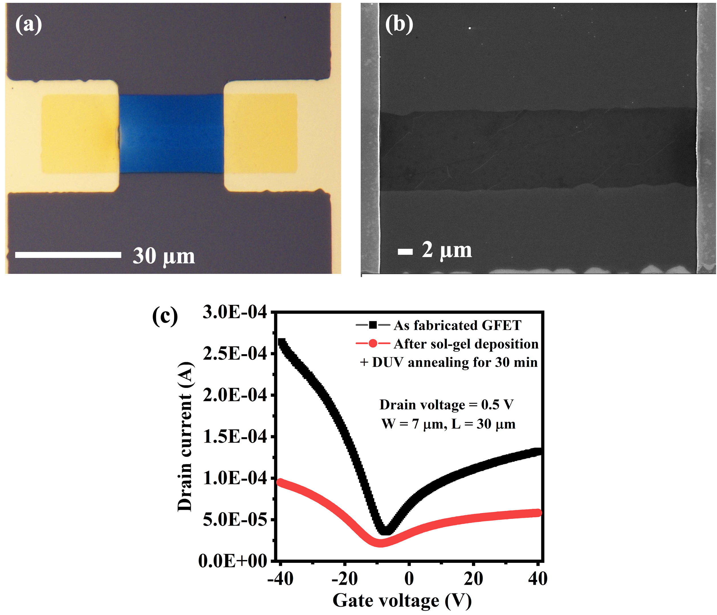
Figure 7 (c) shows the transfer characteristics for the As fabricated GFET and after the DUV annealing with sequential seed layer deposition. The As fabricated GFET shows the Dirac point at around -6.4 V which was the signature of the n-type doping [51]. This shift could be due to long exposure of the resist stripper during lift-off process [52]. The asymmetry in transfer characteristics was due to the work-function difference between Nickel (Work function - 5.01 eV) and graphene (Work function - 4.5 eV) [53]. However, the GFET retains its Dirac point after the DUV annealing in contrast to thermal annealing but with a slight shift in Dirac point towards negative voltage which is at around -8 V. The mobility of the GFET before and after DUV annealing was calculated using the FTM method [9]. The extracted parameters and their comparison are reported in the table I
| Parameters |
|
|
|||||||||
|---|---|---|---|---|---|---|---|---|---|---|---|
|
|
|
|
||||||||
|
4400 | 4281 | 1174 | 1626 | |||||||
|
5.2e11 | 8.9e11 | 7.1e11 | 1.1e12 | |||||||
|
1134 | 3399 | 2084 | 7169 | |||||||
The decrease of the mobility in electron and hole branches after DUV annealing could be attributed to the charged impurity scattering [54]. The summary of the entire work is given in table II.
| Seed layer process | Thickness (nm) | Crack | Dirac point | |||||||||
|
|
|
|
|||||||||
| e-beam | 2.0 nm | Yes | – | – | – | |||||||
| Thickness variation (e-beam) | 2.5 nm | Yes | Yes | – | – | |||||||
| 3.5 nm | Yes | Yes | – | – | ||||||||
| 5.0 nm | No | No | No | No | ||||||||
|
|
– | No | – | Yes | |||||||
IV Conclusion
The comparison between with and without graphene channel devices confirms that the crack issue in sol-gel Alumina layer post thermal annealing is due to underneath graphene layer. The possible mechanism for crack formation was thought to be restoring movement of graphene layer due to stress generated because of TEC mismatch amongst layers and shrinkage during annealing. Even-though DUV annealing with e-beam evaporated thin seed layer films (2.5 nm and 3.5 nm) were not able to resolve the crack issue. On other hand, 5 nm thick e-beam evaporated seed layer based devices did not show crack formation but, electrical testing confirms that the seed layer was not completely oxidised. Finally, we proposed novel two step seed layer deposition process (1.5 nm from e-beam and 1.5 nm from sputtering) with DUV annealing to cover side wall and restrict graphene movement with reduced shrinkage stress. The novel method not only resolved the crack issue but also retained Dirac point of the transistor.
Acknowledgment
This work was carried out under the Centre of Excellence in Nanoelectronics Phase-II project funded by the Ministry of Electronics and Information Technology, Government of India at the IIT Bombay Nanofabrication Facility. SEM imaging of seed layers was carried out at NCPRE and SEM images of GFETs are carried out at IRCC Central Facility at IIT Bombay
References
- [1] K. S. Novoselov, A. K. Geim, S. V. Morozov, D. Jiang, Y. Zhang, S. V. Dubonos, I. V. Grigorieva, and A. A. Firsov, “Electric field effect in atomically thin carbon films,” science, vol. 306, no. 5696, pp. 666–669, 2004.
- [2] J. Lee, L. Tao, K. N. Parrish, Y. Hao, R. S. Ruoff, and D. Akinwande, “Multi-finger flexible graphene field effect transistors with high bendability,” Applied Physics Letters, vol. 101, no. 25, p. 252109, 2012.
- [3] A. A. Balandin, “Thermal properties of graphene and nanostructured carbon materials,” Nature materials, vol. 10, no. 8, pp. 569–581, 2011.
- [4] S. Park, S. H. Shin, M. N. Yogeesh, A. L. Lee, S. Rahimi, and D. Akinwande, “Extremely high-frequency flexible graphene thin-film transistors,” IEEE Electron Device Letters, vol. 37, no. 4, pp. 512–515, 2016.
- [5] S.-J. Han, A. V. Garcia, S. Oida, K. A. Jenkins, and W. Haensch, “Graphene radio frequency receiver integrated circuit,” Nature communications, vol. 5, no. 1, pp. 1–6, 2014.
- [6] Y. Wu, P. Ye, M. A. Capano, Y. Xuan, Y. Sui, M. Qi, J. A. Cooper, T. Shen, D. Pandey, G. Prakash et al., “Top-gated graphene field-effect-transistors formed by decomposition of sic,” Applied Physics Letters, vol. 92, no. 9, p. 092102, 2008.
- [7] J. Kedzierski, P.-L. Hsu, P. Healey, P. W. Wyatt, C. L. Keast, M. Sprinkle, C. Berger, and W. A. De Heer, “Epitaxial graphene transistors on sic substrates,” IEEE Transactions on Electron Devices, vol. 55, no. 8, pp. 2078–2085, 2008.
- [8] X. Wang, S. M. Tabakman, and H. Dai, “Atomic layer deposition of metal oxides on pristine and functionalized graphene,” Journal of the American Chemical Society, vol. 130, no. 26, pp. 8152–8153, 2008.
- [9] S. Kim, J. Nah, I. Jo, D. Shahrjerdi, L. Colombo, Z. Yao, E. Tutuc, and S. K. Banerjee, “Realization of a high mobility dual-gated graphene field-effect transistor with al 2 o 3 dielectric,” Applied Physics Letters, vol. 94, no. 6, p. 062107, 2009.
- [10] B. Fallahazad, K. Lee, G. Lian, S. Kim, C. Corbet, D. Ferrer, L. Colombo, and E. Tutuc, “Scaling of al2o3 dielectric for graphene field-effect transistors,” Applied Physics Letters, vol. 100, no. 9, p. 093112, 2012.
- [11] C. G. Kang, Y. G. Lee, S. K. Lee, E. Park, C. Cho, S. K. Lim, H. J. Hwang, and B. H. Lee, “Mechanism of the effects of low temperature al2o3 passivation on graphene field effect transistors,” Carbon, vol. 53, pp. 182–187, 2013.
- [12] S. Park, C.-H. Kim, W.-J. Lee, S. Sung, and M.-H. Yoon, “Sol-gel metal oxide dielectrics for all-solution-processed electronics,” Materials Science and Engineering: R: Reports, vol. 114, pp. 1–22, 2017.
- [13] C. J. Brinker and G. W. Scherer, Sol-gel science: the physics and chemistry of sol-gel processing. Academic press, 2013.
- [14] B. Wang, W. Huang, L. Chi, M. Al-Hashimi, T. J. Marks, and A. Facchetti, “High-k gate dielectrics for emerging flexible and stretchable electronics,” Chemical reviews, vol. 118, no. 11, pp. 5690–5754, 2018.
- [15] W. Zhu, D. Neumayer, V. Perebeinos, and P. Avouris, “Silicon nitride gate dielectrics and band gap engineering in graphene layers,” Nano letters, vol. 10, no. 9, pp. 3572–3576, 2010.
- [16] M. Xiao, C. Qiu, Z. Zhang, and L.-M. Peng, “Atomic-layer-deposition growth of an ultrathin hfo2 film on graphene,” ACS applied materials & interfaces, vol. 9, no. 39, pp. 34 050–34 056, 2017.
- [17] E. Schilirò, R. Lo Nigro, F. Roccaforte, and F. Giannazzo, “Recent advances in seeded and seed-layer-free atomic layer deposition of high-k dielectrics on graphene for electronics,” C, vol. 5, no. 3, p. 53, 2019.
- [18] A. ZurutuzaáElorza et al., “Highly air stable passivation of graphene based field effect devices,” Nanoscale, vol. 7, no. 8, pp. 3558–3564, 2015.
- [19] T. T. Song, M. Yang, J. W. Chai, M. Callsen, J. Zhou, T. Yang, Z. Zhang, J. S. Pan, D. Z. Chi, Y. P. Feng et al., “The stability of aluminium oxide monolayer and its interface with two-dimensional materials,” Scientific reports, vol. 6, no. 1, pp. 1–9, 2016.
- [20] K. Srinivasan and A. Kottantharayil, “Aluminium oxide thin film deposited by spray coating for p-type silicon surface passivation,” Solar Energy Materials and Solar Cells, vol. 197, pp. 93–98, 2019.
- [21] G.-H. Park, K.-S. Kim, H. Fukidome, T. Suemitsu, T. Otsuji, W.-J. Cho, and M. Suemitsu, “Solution-processed al2o3 gate dielectrics for graphene field-effect transistors,” Japanese Journal of Applied Physics, vol. 55, no. 9, p. 091502, 2016.
- [22] K.-S. Kim, H. Fukidome, and M. Suemitsu, “Direct formation of solution-based al2o3 on epitaxial graphene surface for sensor applications,” Sensors and Materials, vol. 31, no. 7, pp. 2291–2301, 2019.
- [23] T.-E. Bae, H. Kim, J. Jung, and W.-J. Cho, “Fabrication of high-performance graphene field-effect transistor with solution-processed al2o3 sensing membrane,” Applied Physics Letters, vol. 104, no. 15, p. 153506, 2014.
- [24] Y. J. Shin, Y. Wang, H. Huang, G. Kalon, A. T. S. Wee, Z. Shen, C. S. Bhatia, and H. Yang, “Surface-energy engineering of graphene,” Langmuir, vol. 26, no. 6, pp. 3798–3802, 2010.
- [25] R. Singla and A. Kottantharayil, “Stable hydroxyl functionalization and p-type doping of graphene by a non-destructive photo-chemical method,” Carbon, vol. 152, pp. 267–273, 2019.
- [26] J. Wang, J. Binner, Y. Pang, and B. Vaidhyanathan, “Microwave-enhanced densification of sol–gel alumina films,” Thin Solid Films, vol. 516, no. 18, pp. 5996–6001, 2008.
- [27] G. Imamura and K. Saiki, “Modification of graphene/sio2 interface by uv-irradiation: effect on electrical characteristics,” ACS applied materials & interfaces, vol. 7, no. 4, pp. 2439–2443, 2015.
- [28] T. Feng, D. Xie, Y. Lin, H. Tian, H. Zhao, T. Ren, and H. Zhu, “Unipolar to ambipolar conversion in graphene field-effect transistors,” Applied Physics Letters, vol. 101, no. 25, p. 253505, 2012.
- [29] X. Shi, G. Dong, M. Fang, F. Wang, H. Lin, W.-C. Yen, K. S. Chan, Y.-L. Chueh, and J. C. Ho, “Selective n-type doping in graphene via the aluminium nanoparticle decoration approach,” Journal of Materials Chemistry C, vol. 2, no. 27, pp. 5417–5421, 2014.
- [30] K. S. Harsha, Principles of vapor deposition of thin films. Elsevier, 2005.
- [31] F. Volmer, I. Seidler, T. Bisswanger, J.-S. Tu, L. R. Schreiber, C. Stampfer, and B. Beschoten, “How to solve problems in micro-and nanofabrication caused by the emission of electrons and charged metal atoms during e-beam evaporation,” Journal of Physics D: Applied Physics, vol. 54, no. 22, p. 225304, 2021.
- [32] H. L. Brown, S. A. Thornley, S. J. Wakeham, M. J. Thwaites, R. J. Curry, and M. A. Baker, “The impact of substrate bias on a remote plasma sputter coating process for conformal coverage of trenches and 3d structures,” Journal of Physics D: Applied Physics, vol. 48, no. 33, p. 335303, 2015.
- [33] J. E. Lee, G. Ahn, J. Shim, Y. S. Lee, and S. Ryu, “Optical separation of mechanical strain from charge doping in graphene,” Nature communications, vol. 3, no. 1, pp. 1–8, 2012.
- [34] H. Sojoudi, J. Baltazar, C. Henderson, and S. Graham, “Impact of post-growth thermal annealing and environmental exposure on the unintentional doping of cvd graphene films,” Journal of Vacuum Science & Technology B, Nanotechnology and Microelectronics: Materials, Processing, Measurement, and Phenomena, vol. 30, no. 4, p. 041213, 2012.
- [35] H. Kozuka, “Sol-gel ceramic thin film formation: Stress, cracks, radiation striations,” Journal of the Ceramic Society of Japan, vol. 111, no. 1297, pp. 624–632, 2003.
- [36] H. Kozuka, S. Takenaka, H. Tokita, T. Hirano, Y. Higashi, and T. Hamatani, “Stress and cracks in gel-derived ceramic coatings and thick film formation,” Journal of Sol-Gel Science and Technology, vol. 26, no. 1, pp. 681–686, 2003.
- [37] H. Kozuka, “Stress evolution on gel-to-ceramic thin film conversion,” Journal of sol-gel science and technology, vol. 40, no. 2, pp. 287–297, 2006.
- [38] Y.-H. Kim, J.-S. Heo, T.-H. Kim, S. Park, M.-H. Yoon, J. Kim, M. S. Oh, G.-R. Yi, Y.-Y. Noh, and S. K. Park, “Flexible metal-oxide devices made by room-temperature photochemical activation of sol–gel films,” Nature, vol. 489, no. 7414, pp. 128–132, 2012.
- [39] S. Park, K.-H. Kim, J.-W. Jo, S. Sung, K.-T. Kim, W.-J. Lee, J. Kim, H. J. Kim, G.-R. Yi, Y.-H. Kim et al., “In-depth studies on rapid photochemical activation of various sol–gel metal oxide films for flexible transparent electronics,” Advanced Functional Materials, vol. 25, no. 19, pp. 2807–2815, 2015.
- [40] J.-W. Jo, Y.-H. Kim, J. Park, J. S. Heo, S. Hwang, W.-J. Lee, M.-H. Yoon, M.-G. Kim, and S. K. Park, “Ultralow-temperature solution-processed aluminum oxide dielectrics via local structure control of nanoclusters,” ACS applied materials & interfaces, vol. 9, no. 40, pp. 35 114–35 124, 2017.
- [41] C.-Y. Huang, L.-K. Xiao, Y.-H. Chang, L.-Y. Chen, G.-T. Chen, and M.-H. Li, “High-performance solution-processed znsno metal–semiconductor–metal ultraviolet photodetectors via ultraviolet/ozone photo-annealing,” Semiconductor Science and Technology, vol. 36, no. 9, p. 095013, 2021.
- [42] K.-S. Kim, G.-H. Park, H. Fukidome, T. Suemitsu, T. Otsuji, W.-J. Cho, and M. Suemitsu, “Solution-based formation of high-quality gate dielectrics on epitaxial graphene by microwave-assisted annealing,” Japanese Journal of Applied Physics, vol. 56, no. 6S1, p. 06GF09, 2017.
- [43] Y. Kim, D.-H. Cho, S. Ryu, and C. Lee, “Tuning doping and strain in graphene by microwave-induced annealing,” Carbon, vol. 67, pp. 673–679, 2014.
- [44] Y. S. Rim, W. H. Jeong, D. L. Kim, H. S. Lim, K. M. Kim, and H. J. Kim, “Simultaneous modification of pyrolysis and densification for low-temperature solution-processed flexible oxide thin-film transistors,” Journal of Materials Chemistry, vol. 22, no. 25, pp. 12 491–12 497, 2012.
- [45] P. Blake, E. Hill, A. Castro Neto, K. Novoselov, D. Jiang, R. Yang, T. Booth, and A. Geim, “Making graphene visible,” Applied physics letters, vol. 91, no. 6, p. 063124, 2007.
- [46] B. Gaweł, K. Gaweł, and G. Øye, “Sol-gel synthesis of non-silica monolithic materials,” Materials, vol. 3, no. 4, pp. 2815–2833, 2010.
- [47] D. Yoon, Y.-W. Son, and H. Cheong, “Negative thermal expansion coefficient of graphene measured by raman spectroscopy,” Nano letters, vol. 11, no. 8, pp. 3227–3231, 2011.
- [48] W. Bao, F. Miao, Z. Chen, H. Zhang, W. Jang, C. Dames, and C. N. Lau, “Controlled ripple texturing of suspended graphene and ultrathin graphite membranes,” Nature nanotechnology, vol. 4, no. 9, pp. 562–566, 2009.
- [49] A. Wilson, “The thermal expansion of aluminium from 0 to 650 c,” Proceedings of the Physical Society, vol. 53, no. 3, p. 235, 1941.
- [50] T. Jiang, Z. Wang, X. Ruan, and Y. Zhu, “Equi-biaxial compressive strain in graphene: Grüneisen parameter and buckling ridges,” 2D Materials, vol. 6, no. 1, p. 015026, 2018.
- [51] B. Guo, L. Fang, B. Zhang, and J. R. Gong, “Graphene doping: a review,” Insciences J., vol. 1, no. 2, pp. 80–89, 2011.
- [52] O. Sul, K. Kim, E. Choi, J. Kil, W. Park, and S.-B. Lee, “Reduction of hole doping of chemical vapor deposition grown graphene by photoresist selection and thermal treatment,” Nanotechnology, vol. 27, no. 50, p. 505205, 2016.
- [53] K. Nagashio, T. Nishimura, K. Kita, and A. Toriumi, “Metal/graphene contact as a performance killer of ultra-high mobility graphene analysis of intrinsic mobility and contact resistance,” in 2009 IEEE International Electron Devices Meeting (IEDM). Ieee, 2009, pp. 1–4.
- [54] J.-H. Chen, C. Jang, S. Adam, M. Fuhrer, E. D. Williams, and M. Ishigami, “Charged-impurity scattering in graphene,” Nature physics, vol. 4, no. 5, pp. 377–381, 2008.