Self-sealing complex oxide resonators
Abstract
Although 2D materials hold great potential for next-generation pressure sensors, recent studies revealed that gases permeate along the membrane-surface interface that is only weakly bound by van der Waals interactions, necessitating additional sealing procedures. In this work, we demonstrate the use of free-standing complex oxides as self-sealing membranes that allow the reference cavity of pressure sensors to be sealed by a simple anneal. To test the hermeticity, we study the gas permeation time constants in nano-mechanical resonators made from \chSrRuO3 and \chSrTiO3 membranes suspended over \chSiO2/Si cavities which show an improvement up to 4 orders of magnitude in the permeation time constant after annealing the devices for 15 minutes. Similar devices fabricated on \chSi3N4/Si do not show such improvements, suggesting that the adhesion increase over \chSiO2 is mediated by oxygen bonds that are formed at the \chSiO2/complex oxide interface during the self-sealing anneal. We confirm the enhancement of adhesion by picosecond ultrasonics measurements which show an increase in the interfacial stiffness by 70% after annealing. Since it is straigthforward to apply, the presented self-sealing method is thus a promising route toward realizing ultrathin hermetic pressure sensors.
I Introduction
Van der Waals (vdW) materials attracted significant attention in the microelectromechanical systems (MEMS) community due to their low dimensionality, flexibility and strength [1]. In particular, graphene is considered as the material for the next generation pressure sensors [2, 3, 4, 5, 6, 7] thanks to its intrinsic impermeability to gases [8, 9, 10]. Pressure sensors operate by measuring the deflection of a membrane due to the pressure difference between a reference cavity and the environment. For a reliable pressure sensor, hermeticity of the cavity underneath the membrane is essential. However, gas permeation along the interface between the vdW membrane and the substrate causes pressure variations in the reference cavity, which renders the pressure readings from graphene-based pressure sensors unreliable [11, 12].
Recently reported sealing protocols have enabled improvements in the hermeticity of vdW material membranes of up to a factor 10000 [11, 12], but scaling them to high volume production is difficult, since depositing and patterning of sealing layers on top of ultrathin vdW material membranes is often detrimental to device performance, in particular if high temperatures are needed. Moreover, the pressure at which the sealing layer is deposited is often fixed by the process, such that the reference pressure in the cavity cannot be freely controlled [13, 14, 15, 16].
As an alternative to graphene, we introduce in this letter, free-standing single crystal complex oxide perovskites as a membrane for pressure sensing MEMS applications. Thanks to their inter-unit cell chemical bonds and the ability to form new ones at high temperatures [17], they promise a stronger adhesion to the substrate than 2D materials which are mediated by a vdW gap. Moreover, due to their epitaxial crystalline growth, extremely flat layer surfaces can be grown using pulsed laser deposition, enhancing the interface contact and reducing the formation probability of gas leakage pathways. Recent developments in releasing epitaxially grown single crystal complex oxides allow them to be thinned down to the unit cell limit, similar to the vdW materials [18, 19, 20]. Complex oxides in their ultra-thin free-standing form are mechanically robust [21] while withstanding strains up to 8% [22, 23], are flexible enough to allow large curvatures [24] and have already been demonstrated as viable nanomechanical resonators [25, 26]. Furthermore, wafer-scale production of single crystalline complex oxides are being developed [27] which makes them even more appealing for large-scale CMOS compatible fabrication.
Here, we use free-standing \chSrRuO3 (SRO) and \chSrTiO3 (STO) suspended over \chSiO2/Si cavities to make pressure sensors and demonstrate a simple, CMOS compatible sealing technique which does not require additional fabrication steps. The sealing consists of annealing the devices above 300 ∘C in ambient conditions for 15 minutes. We measure the time dependence of the resonance frequency to extract the gas permeation time constant. By comparing the permeation time constant of the pressure sensor devices before and after performing the self-sealing annealing process, we show that the permeation time constant increases from 14 s to 10000 s, indicative of a large increase in hermeticity. Comparable devices fabricated on \chSi3N4/Si cavities do not show such enhancement of the hermeticity which suggests that the improved hermeticity is mediated by the properties of the \chSiO2 that promote adhesion to the complex oxides, thus eliminating gas leakage rates. Furthermore, we probe the STO-\chSiO2 interface in both annealed and non-annealed samples using a picosecond ultrasonics technique. The measurements show a clear reduction in the ultrasonic reflection coefficient at the interface between STO-\chSiO2 after the annealing procedure, indicative of an increased adhesion. Our work investigates the use of ultrathin complex oxide membranes for pressure sensors, and demonstrates self-sealing of the interface after transfer, thus providing an alternative to graphene and MEMS sensor technologies.
II Results
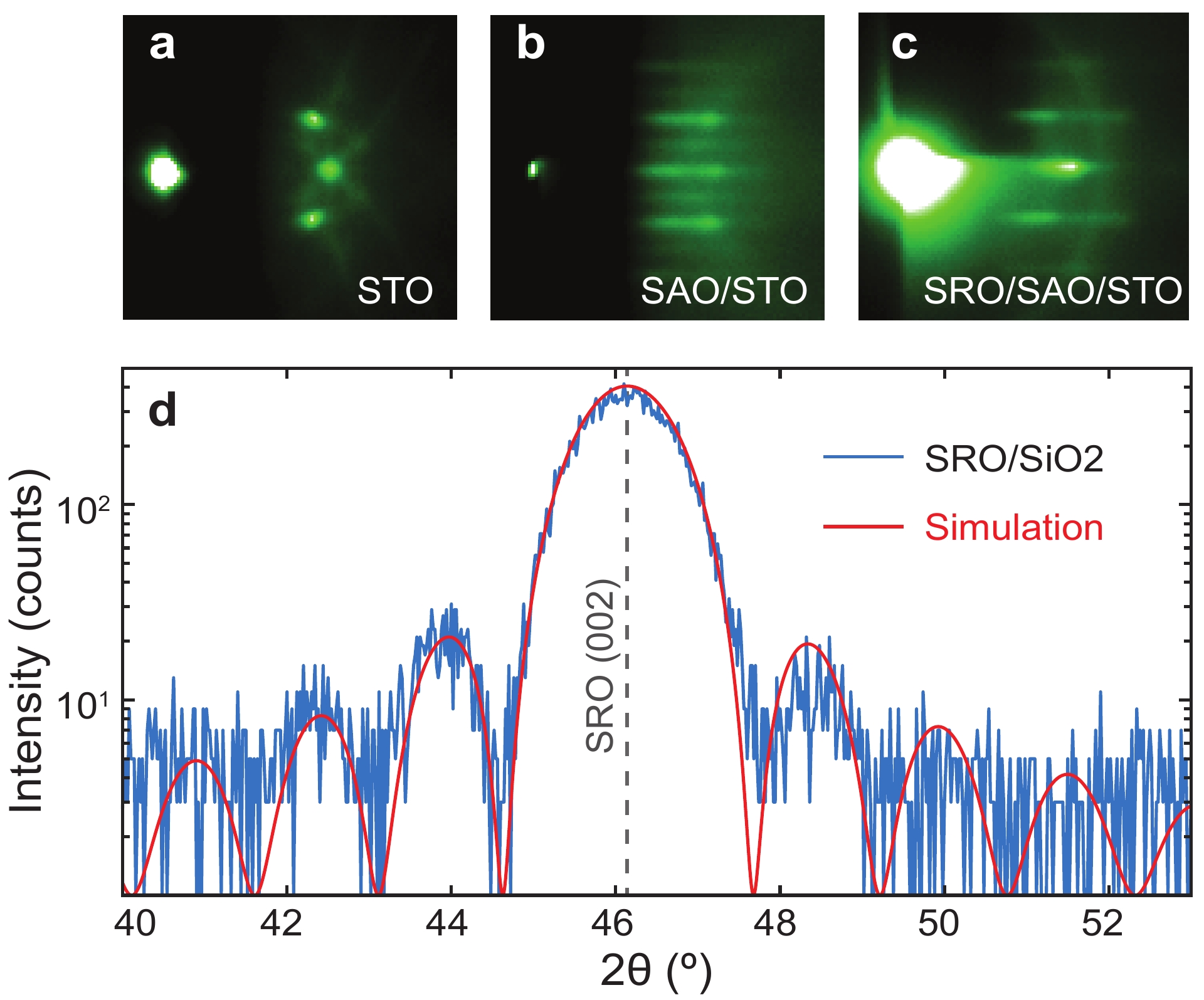
Crystalline free-standing complex oxides are synthesized using pulsed-laser deposition by growing a (water-soluble) buffer layer of \chSr3Al2O6 (SAO) on \chSrTiO3 (001) substrates, followed by an overlayer of choice (STO or SRO). The growth is monitored by in-situ reflection high energy electron diffraction (RHEED), confirming 2D growth (Fig. 1a-c). After growth, the samples are attached to polydimethyl siloxane (PDMS) films for support during the etching process of the buffer layer which is performed by submerging the PDMS covered sample in deionized water for 24 hours. After the SAO is etched away, the film of choice can be transferred onto a dummy \chSiO2/Si substrate using a deterministic transfer method [28] for characterization. See supplementary information (S.I-III).
We perform X-ray diffraction (XRD) measurements on the films after transferring parts of them to a dummy \chSiO2/Si to verify the film thicknesses and the crystal coherence. As shown in Fig. 1d, the crystallographic (002) peak of SRO can be identified with finite size oscillations on both sides of the main peak, showing long-range crystal coherence of the film after exfoliation and the transfer process. A model fit plotted in red on top of the XRD data, is used to extract the c-axis lattice parameter as well as the number of pseudo-cubic unit cells. In the case of SRO (Fig. 1d), the model yields a thickness of 16 unit cells (u.c.) with a c-axis lattice parameter of 3.931 Å, in good agreement with the value reported in the literature [29]. After confirming the crystallinity and the thickness of the films, we transfer individual flakes of SRO (6.3 nm) and STO (82 nm) on top of a pre-patterned \chSiO2/Si substrate with circular cavities with diameters from 3 µm to 10 µm, using the vdW pick up technique [30, 31]. Cavities are defined in thermally grown \chSiO2 of 285 nm in thickness using e-beam lithography followed by reactive ion etching down to the Si layer [11].
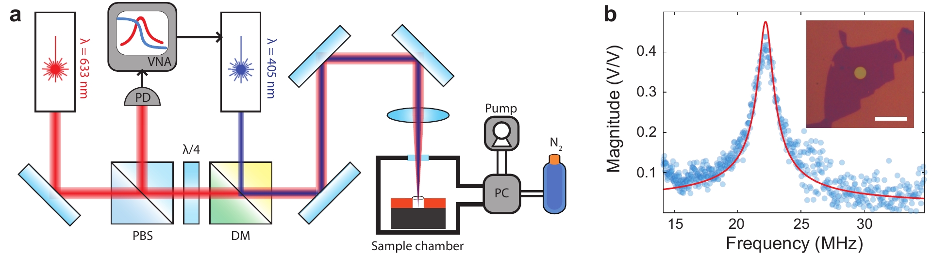
Once the fabrication of suspended complex oxide membranes are completed, we measure the pressure dependence of the resonance frequencies using a laser interferometry technique as illustrated in Fig. 2a. An intensity modulated blue ( = 405 nm) laser excites the motion of the membrane which is situated in a pressure controlled environment. A continuous red laser ( = 633 nm) monitors the movement of the membrane. The reflected signal is collected by a photo detector (PD) and the signal is sent to a vector network analyser (VNA). Figure 2b shows an example resonance peak of a SRO flake suspended over a circular \chSiO2/Si cavity (see inset). A harmonic oscillator function is fitted to the data (red) which is used to extract the resonance frequency as a function of sample chamber (SC) pressure.
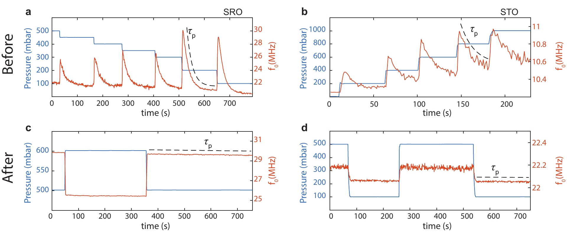
The time dependent resonance frequency of SRO and STO devices directly after transfer over the cavities are shown in Fig. 3a-b. The SC pressures are adjusted in a step-wise fashion while the frequency is swept to capture the resonance peak. After fitting the data to a harmonic oscillator function, the resonance frequency is extracted and plotted (orange, right y-axis). Before the sealing procedure, both SRO and STO membranes show, after the pressure changes, sudden increases in the resonance frequencies followed by exponential decays of time constant . This behavior suggests that the membranes are tensioned due to the change in the pressure difference in and outside of the cavity, which then quickly equilibrates due to the permeation of gas molecules. In both SRO and STO, the average permeation time constants are approximately 21 s and 14 s respectively (see S.IV for details on the analysis).
To reduce the gas leakage, a self-sealing procedure was performed, in which the samples are annealed in air at atmospheric pressure at elevated temperature (for 1 hour at 300 ∘C for SRO and for 15 minutes at 400 ∘C for STO). After this procedure, the measurements from Fig. 3a,b are repeated for both SRO and STO samples and shown in Fig. 3c and 3d respectively. The sudden spike in the resonance frequency followed by a fast decay is not observed in Fig. 3c but instead, a slow reduction in the resonance frequency can be seen. By fitting an exponential decay to the slow reduction in the resonance frequency, we find a of 1.1 104 s. Similar behaviour is observed in the STO device after annealing for 15 minutes at 400 ∘C. Before annealing, the mean permeation time constants of STO is = 13.9 s, which increases to 1.2 105 s after a self-sealing procedure. As shown in Fig. 3d, no observable decay in the resonance frequencies is present but there are small drifts. It is worth mentioning that due to the minute variations in the resonance frequency, fitting the data from Fig. 3c&d to an exponential decay is difficult and results in large fit errors. However, we estimate a lower bound of 103 s.
Next, the adhesion at the interface of complex oxides and the substrate is further tested using a picosecond ultrasonics method. An ultra-fast optical pump-probe setup is used to generate and detect GHz acoustic waves in solids. This allows characterization of the adhesion between the thin layer and the substrate, since these waves are sensitive to the boundary conditions at the interface between two different materials [32, 33, 34]. For example, this method is used to probe the adhesion properties of metal layers evaporated on glass surfaces [33] or to characterize the adhesion of vdW materials [35].
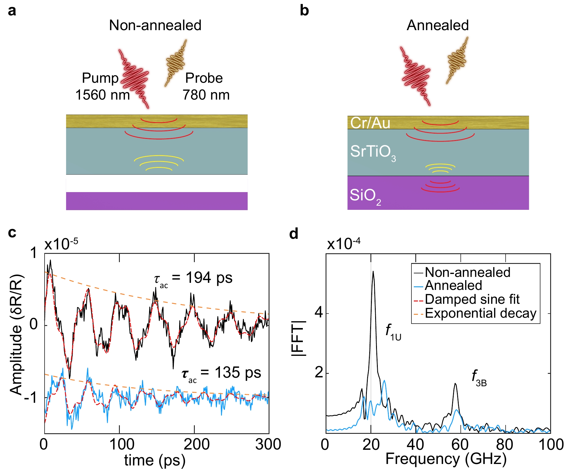
We prepare two sets of flakes on \chSiO2/Si transferred from the same batch of STO (thickness 82 nm). One set is untreated (Fig. 4a) while the other is treated with the self-sealing procedure for 1 hour at 400 ∘C (Fig. 4b). Both substrates containing STO flakes are then coated with 33 nm of Au/Cr for optical pumping and probing (see S.XI for details). We use an asynchronous optical sampling (ASOPS) technique with a 1560 nm pump laser pulse and a 780 nm probe pulse laser to optothermomechanically generate and detect acoustic echos into individual STO flakes on timescales ranging from 1 ps to 10 ns. The duration of the pulses of both lasers is around 100 fs. Measurements are performed on 4 non-annealed and 5 annealed flakes. An example of the acoustic measurements on a non-annealed (black) and an annealed (light blue) STO flakes is presented in Fig. 4c-d. The overall results are reported in Table 1.
The acoustic wave echos inside the Au/Cr/STO assembly can be seen for the non-annealed and annealed cases in Fig. 4c. The decay of the amplitudes of the measurements in the different flakes (Fig. 4c for example) are fitted with a damped sine-wave to obtain the time constant of the envelope, which characterizes the decay rate of the waves due to reflections at the interface with the substrate, wherein acoustic energy is transmitted. This results in an average value of = 220 ps for the non-annealed flakes and = 114 ps for the annealed flakes (see Table 1). From these values of , we calculate the associated acoustic reflection coefficient [35] , at the STO/\chSiO2 interface. An average value of = 0.81 is found for the non-annealed flakes and = 0.70 for the annealed flakes. These reflection coefficients allow the calculation of their associated interfacial stiffnesses , which are a direct measure of the adhesion at the interface; a higher corresponds to a stronger adhesion (see S.XI. for more information). A value of = 2.30 1018 N/m3 is found for the annealed flakes, which is larger than that of the non-annealed flakes, = 1.33 1018 N/m3. After annealing, the interfacial stiffness increases, resulting in a better transmission of the acoustic energy to the \chSiO2/Si substrate during the successive reflections of the acoustic waves inside the Au/Cr/STO assembly, and therefore to a weaker reflection coefficient and a faster decay in amplitude.
Figure 4d shows the Fourier transform of the temporal data in Fig. 4c revealing that they are composed of 2 distinct frequencies. The low frequency (22 GHz) corresponds to the first mode of standing waves in the Au/Cr/STO assembly unbound from the underlying \chSiO2, calculated theoretically (see S.XI for details) at = 21 GHz. The higher frequency (57 GHz) likely corresponds to the third mode of the standing waves in the bounded assembly (calculated = 53 GHz). The difference between the theoretical values and the experimental ones could be caused by small variations in the thickness of the Au/Cr/STO assembly and by the value of the longitudinal sound velocities used to calculate these frequencies taken from the literature (see S.XI). In both samples, the presence of frequencies corresponding to unbounded () and bounded () cases shows that the adhesion here is intermediate [35] (between perfect contact and total debonding). However, the amplitude of the components in the annealed case are weaker than in the non-annealed case (Fig. 4d), since their attenuation by transmission of the acoustic energy to the substrate through multiple reflections in the Au/Cr/STO assembly is higher (difference in , Fig. 4c). The increased adhesion found from these ultra-fast picosecond ultrasonics measurements is consistent with the increased hermeticity observed in Fig. 3.
| (ps) | (1018 N/m3) | ||
| Non-annealed (4 flakes) | 219.9 50.0 | 0.81 0.04 | 1.33 0.20 |
| Annealed (5 flakes) | 113.6 17.1 | 0.70 0.04 | 2.30 0.64 |
| Theoretical values | 59 (perfect contact) (total debonding) | 0.45 (perfect contact) 1 (total debonding) | >20 (perfect contact) <0.1 (total debonding) |
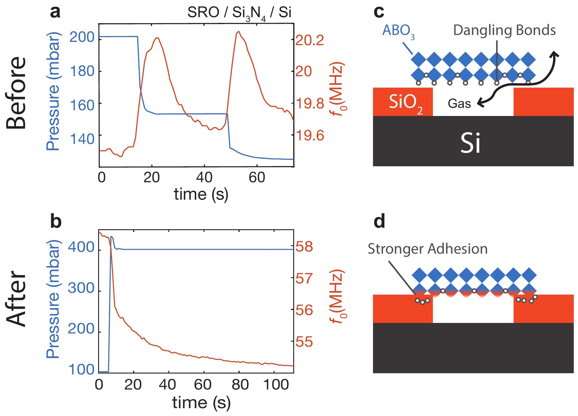
Having used mechanical resonance measurements and picosecond ultrasonics measurements to establish the enhancement of the adhesion at the interface of complex oxides and \chSiO2, we now move on to investigate whether the observed adhesion increase is unique to the \chSiO2 substrate. For this purpose, we performed additional permeation measurements on nominally identical samples made on an oxygen-free substrate, \chSi3N4/Si. Figures 5a&b, show the time dependence of the resonance frequency of a SRO flake suspended over a cavity etched in \chSi3N4/Si. Figure 5a is taken before annealing and Fig. 5b is taken after annealing for 1 hour at 400 ∘C. Before annealing, the permeation time constant is = 6.02 s and after annealing for 1 hour, it increases to = 22.5 s. Although a factor of 3.7 improvement is observed, the absolute leakage time constant after annealing in \chSi3N4 devices are on the order of those in \chSiO2 devices even before annealing (see S.V for the analysis on ). Investigation by means of energy dispersive X-ray spectroscopy (EDX) ruled out any role of SAO residues in the adhesion (see S.VI). The absence of the Al peak in the EDX spectra strongly suggests that SAO is indeed fully removed by water. Due to above reasons we hypothesize that the improved bonding is mediated by the presence of oxygen in the \chSiO2 substrate. A possible scenario is illustrated in Fig. 5c-d where the adhesion is enhanced by the reaction between dangling bonds at the bottom of the complex oxide flake and the oxygen rich substrate at elevated temperatures.
Furthermore, it is worth to note the longevity of the improved adhesion on top of the \chSiO2 substrate. We have performed pick-up techniques widely used in the fabrication of vdW heterostructures using both polypropylene carbonate (PPC) and polycarbonate (PC), the latter of which has stronger adhesive properties and is thus more suitable for monolayer transfer [30, 36, 37]. Non-annealed samples of SRO on \chSiO2 were easily picked up using both PPC and PC while the samples annealed 8 months ago and stored in ambient conditions, could not be removed from the substrate (see S.VIII). Unlike vdW materials which can be detached from the substrate after annealing and subsequently storing in ambient conditions, the improvement in the adhesion seems to be longer-lasting in annealed oxides.
III Discussion & Conclusion
Although graphene and its family of vdW materials have demonstrated superior pressure sensing capabilities [1] compared to the state-of-the-art made from Si [6], the leakage through the vdW gap between the material and the substrate still remains a key challenge to overcome. Previous works have shown that the hermeticity can be improved by e.g. ironing with a diamond atomic force microscopy (AFM) tip [12] or electron-beam induced deposition of \chSiO2 [11]. Unfortunately, both the AFM and EBID methods are not scalable, since they are too slow to apply over large areas. Furthermore, if only the edge of the flake is sealed, and there is a puncture in a sealed flake, then all of the cavities underneath the flake are effectively vented. The intrinsic vdW nature and the difficulty in producing pin-hole free 2D materials are the hurdles in fabricating reliable hermetically sealed pressure sensors.
The annealing procedure performed on the single crystal complex oxide flakes on \chSiO2 improves the hermeticity of the cavity as measured by mechanics and improves mechanical contact as measured by picosecond ultrasonics. Furthermore, the PC pick-up technique widely used in the fabrication of the vdW heterostructures is ineffective in removing the annealed flakes from \chSiO2 even after 8 months of storage in ambient conditions. Therefore we can conclude that after the self-sealing procedure the adhesion is better and contact between the PLD layer and the substrate is more intimate. This increase can be caused by removal of water, and by formation of chemical bonds. Both mechanisms might play a role. However, the permeation time constant does not seem to increase by comparable magnitudes in samples created on \chSi3N4/Si substrates. This seems to suggest that chemical bond formation is the most likely, as water removal will likely happen for both substrates. This mechanism is similar to direct wafer-to-wafer bonding techniques that are in widespread use in the semiconductor industry [38, 39, 40, 41, 42].
Thanks to the advent of the water-releasing technique [18], free-standing single-crystal complex oxides can be synthesized and transferred onto cavities for MEMS applications as presented in this work. One key difference between vdW materials and free-standing complex oxides is the existence of interlayer covalent bonds. We propose that by controlling the concentration of oxygen vacancies in the complex oxide, the density of dangling bonds at the surface can be tuned. Therefore, we expect to be able to further improve the adhesion - thus the hermeticity - by optimizing the annealing conditions. Yong et al. have shown that at temperatures above 750 ∘C and pressures below 400 mTorr, interfacial species of \chTiSi2 and/or \chSrSiO3 form at the STO-\chSiO2 interface [17]. We believe similar effects may be happening in our flakes although our annealing temperatures and \chO2 partial pressures are quite different.
In summary, we have investigated the use of free-standing complex oxides \chSrRuO3 and \chSrTiO3 for pressure sensing applications and presented a self-sealing method based on annealing to improve the hermeticity of complex oxide based pressure sensors. Gases permeate along the vdW - substrate interface and the elimination of this leakage path is a key towards fabricating next generation pressure sensors. We realized a leap towards this goal by promoting stronger adhesion to form at the interface of complex oxides and \chSiO2. Improvements in the gas permeation time constant as well as the contrast in the acoustic impedance at the interface suggest that the interface adhesion of complex oxides (\chSrRuO3 and \chSrTiO3), and \chSiO2 is stronger after annealing. We further investigated the effect of the substrate on the interfacial adhesion by performing the permeation measurements on devices made on \chSi3N4/Si. Since significant improvements in time constant are only observed on \chSiO2 substrate, it is likely that the oxygen atoms on the \chSiO2 substrate surface play an important role in mediating the adhesion. Our work presents a first step towards implementing free-standing complex oxides as an alternative to silicon and 2D materials in next generation MEMS and NEMS sensors.
Acknowledgements.
M.L., H.S.J.v.d.Z. and P.G.S. acknowledge funding from the European Union’s Horizon 2020 research and innovation program under grant agreement number 881603. A.D.C. acknowledges funding from Quantox of QuantERA ERA-NET Cofund in Quantum Technologies and by the Netherlands Organisation for Scientific Research (NWO/OCW) as part of the VIDI program. G.V. acknowledges support from project TKI-HTSM/19.0172.References
- [1] M. C. Lemme, S. Wagner, K. Lee, X. Fan, G. J. Verbiest, S. Wittmann, S. Lukas, R. J. Dolleman, F. Niklaus, H. S. J. van der Zant, G. S. Duesberg, and P. G. Steeneken, “Nanoelectromechanical sensors based on suspended 2D materials,” Research, vol. 2020, 2020.
- [2] R. J. Dolleman, D. Davidovikj, S. J. Cartamil-Bueno, H. S. J. van der Zant, and P. G. Steeneken, “Graphene squeeze-film pressure sensors,” Nano letters, vol. 16, no. 1, pp. 568–571, 2016.
- [3] A. D. Smith, F. Niklaus, A. Paussa, S. Vaziri, A. C. Fischer, M. Sterner, F. Forsberg, A. Delin, D. Esseni, P. Palestri, M. Östling, and M. C. Lemme, “Electromechanical piezoresistive sensing in suspended graphene membranes,” Nano letters, vol. 13, no. 7, pp. 3237–3242, 2013.
- [4] A. D. Smith, F. Niklaus, A. Paussa, S. Schröder, A. C. Fischer, M. Sterner, S. Wagner, S. Vaziri, F. Forsberg, D. Esseni, M. Östlin, and M. C. Lemme, “Piezoresistive properties of suspended graphene membranes under uniaxial and biaxial strain in nanoelectromechanical pressure sensors,” ACS nano, vol. 10, no. 11, pp. 9879–9886, 2016.
- [5] S.-E. Zhu, M. Krishna Ghatkesar, C. Zhang, and G. C. A. M. Janssen, “Graphene based piezoresistive pressure sensor,” Applied Physics Letters, vol. 102, no. 16, p. 161904, 2013.
- [6] M. Šiškins, M. Lee, D. Wehenkel, R. van Rijn, T. W. de Jong, J. R. Renshof, B. C. Hopman, W. S. J. M. Peters, D. Davidovikj, H. S. J. van der Zant, and P. G. Steeneken, “Sensitive capacitive pressure sensors based on graphene membrane arrays,” Microsystems & Nanoengineering, vol. 6, no. 1, pp. 1–9, 2020.
- [7] D. Davidovikj, P. H. Scheepers, H. S. J. Van Der Zant, and P. G. Steeneken, “Static capacitive pressure sensing using a single graphene drum,” ACS applied materials & interfaces, vol. 9, no. 49, pp. 43205–43210, 2017.
- [8] V. Berry, “Impermeability of graphene and its applications,” Carbon, vol. 62, pp. 1–10, 2013.
- [9] J. S. Bunch, S. S. Verbridge, J. S. Alden, A. M. Van Der Zande, J. M. Parpia, H. G. Craighead, and P. L. McEuen, “Impermeable atomic membranes from graphene sheets,” Nano letters, vol. 8, no. 8, pp. 2458–2462, 2008.
- [10] P. Z. Sun, Q. Yang, W. J. Kuang, Y. V. Stebunov, W. Q. Xiong, J. Yu, R. R. Nair, M. I. Katsnelson, S. J. Yuan, I. V. Grigorieva, M. Lozada-Hidalgo, F. C. Wang, and A. K. Geim, “Limits on gas impermeability of graphene,” Nature, vol. 579, no. 7798, pp. 229–232, 2020.
- [11] M. Lee, D. Davidovikj, B. Sajadi, M. Šiškins, F. Alijani, H. S. J. van der Zant, and P. G. Steeneken, “Sealing graphene nanodrums,” Nano letters, vol. 19, no. 8, pp. 5313–5318, 2019.
- [12] Y. Manzanares-Negro, P. Ares, M. Jaafar, G. Lopez-Polin, C. Gomez-Navarro, and J. Gomez-Herrero, “Improved graphene blisters by ultrahigh pressure sealing,” ACS Applied Materials & Interfaces, vol. 12, no. 33, pp. 37750–37756, 2020.
- [13] O. Wunnicke, H. Kwinten, L. van Leuken-Peters, M. In’t Zandt, K. Reimann, V. Aravindh, H. M. R. Suy, M. J. Goossens, R. A. M. Wolters, W. F. A. Besling, J. T. M. van Beek, and P. G. Steeneken, “Small, low-ohmic RF MEMS switches with thin-film package,” in 2011 IEEE 24th International Conference on Micro Electro Mechanical Systems, pp. 793–796, IEEE, 2011.
- [14] A. Partridge, M. Lutz, B. Kim, M. Hopcroft, R. N. Candler, T. W. Kenny, K. Petersen, and M. Esashi, “MEMS resonators: getting the packaging right,” in Proc. SEMICON, pp. 55–58, 2005.
- [15] A. Partridge, A. E. Rice, T. W. Kenny, and M. Lutz, “New thin film epitaxial polysilicon encapsulation for piezoresistive accelerometers,” in Technical Digest. MEMS 2001. 14th IEEE International Conference on Micro Electro Mechanical Systems (Cat. No. 01CH37090), pp. 54–59, IEEE, 2001.
- [16] K. Seetharaman, B. van Velzen, J. van Wingerden, H. van Zadelhoff, C. Yuan, F. Rietveld, C. Tak, J. van Beek, P. H. Magnée, and H. C. Beijerinck, “A robust thin-film wafer-level packaging approach for MEMS devices,” Journal of microelectronics and electronic packaging, vol. 7, no. 3, pp. 175–180, 2010.
- [17] G. Yong, R. M. Kolagani, S. Adhikari, W. Vanderlinde, Y. Liang, K. Muramatsu, and S. Friedrich, “Thermal stability of \chSrTiO3/SiO2/Si interfaces at intermediate oxygen pressures,” Journal of Applied Physics, vol. 108, no. 3, p. 033502, 2010.
- [18] D. Lu, D. J. Baek, S. S. Hong, L. F. Kourkoutis, Y. Hikita, and H. Y. Hwang, “Synthesis of freestanding single-crystal perovskite films and heterostructures by etching of sacrificial water-soluble layers,” Nature materials, vol. 15, no. 12, pp. 1255–1260, 2016.
- [19] D. Ji, S. Cai, T. R. Paudel, H. Sun, C. Zhang, L. Han, Y. Wei, Y. Zang, M. Gu, Y. Zhang, W. Gao, H. Huyan, W. Guo, D. Wu, Z. Gu, E. Y. Tsymbal, P. Wang, Y. Nie, and X. Pan, “Freestanding crystalline oxide perovskites down to the monolayer limit,” Nature, vol. 570, no. 7759, pp. 87–90, 2019.
- [20] H. S. Kum, H. Lee, S. Kim, S. Lindemann, W. Kong, K. Qiao, P. Chen, J. Irwin, J. H. Lee, S. Xie, S. Subramanian, J. Shim, S.-H. Bae, C. Choi, L. Ranno, S. Seo, S. Lee, J. Bauer, H. Li, K. Lee, J. A. Robinson, C. A. Ross, D. G. Schlom, M. S. Rzchowski, C.-B. Eom, and J. Kim, “Heterogeneous integration of single-crystalline complex-oxide membranes,” Nature, vol. 578, no. 7793, pp. 75–81, 2020.
- [21] V. Harbola, S. Crossley, S. S. Hong, D. Lu, Y. A. Birkhölzer, Y. Hikita, and H. Y. Hwang, “Strain gradient elasticity in \chSrTiO3 membranes: Bending versus stretching,” Nano letters, vol. 21, no. 6, pp. 2470–2475, 2021.
- [22] S. S. Hong, M. Gu, M. Verma, V. Harbola, B. Y. Wang, D. Lu, A. Vailionis, Y. Hikita, R. Pentcheva, J. M. Rondinelli, and H. Y. Hwang, “Extreme tensile strain states in \chLa0.7Ca0.3MnO3 membranes,” Science, vol. 368, no. 6486, pp. 71–76, 2020.
- [23] R. Xu, J. Huang, E. S. Barnard, S. S. Hong, P. Singh, E. K. Wong, T. Jansen, V. Harbola, J. Xiao, B. Y. Wang, S. Crossley, D. Lu, S. Liu, and H. H. Y., “Strain-induced room-temperature ferroelectricity in \chSrTiO3 membranes,” Nature communications, vol. 11, no. 1, pp. 1–8, 2020.
- [24] B. Peng, R.-C. Peng, Y.-Q. Zhang, G. Dong, Z. Zhou, Y. Zhou, T. Li, Z. Liu, Z. Luo, S. Wang, Y. Xia, R. Qiu, X. Cheng, F. Xue, Z. Hu, W. Ren, Z.-G. Ye, L.-Q. Chen, Z. Shan, T. Min, and M. Liu, “Phase transition enhanced superior elasticity in freestanding single-crystalline multiferroic \chBiFeO3 membranes,” Science advances, vol. 6, no. 34, p. eaba5847, 2020.
- [25] D. Davidovikj, D. J. Groenendijk, A. M. R. V. L. Monteiro, A. Dijkhoff, D. Afanasiev, M. Šiškins, M. Lee, Y. Huang, E. van Heumen, H. S. J. van der Zant, A. D. Caviglia, and P. G. Steeneken, “Ultrathin complex oxide nanomechanical resonators,” Communications Physics, vol. 3, no. 1, pp. 1–6, 2020.
- [26] N. Manca, G. Mattoni, M. Pelassa, W. J. Venstra, H. S. J. van der Zant, and A. D. Caviglia, “Large tunability of strain in \chWO3 single-crystal microresonators controlled by exposure to \chH2 gas,” ACS applied materials & interfaces, vol. 11, no. 47, pp. 44438–44443, 2019.
- [27] D. H. A. Blank, M. Dekkers, and G. Rijnders, “Pulsed laser deposition in twente: from research tool towards industrial deposition,” Journal of physics D: applied physics, vol. 47, no. 3, p. 034006, 2013.
- [28] A. Castellanos-Gomez, M. Buscema, R. Molenaar, V. Singh, L. Janssen, H. S. J. Van Der Zant, and G. A. Steele, “Deterministic transfer of two-dimensional materials by all-dry viscoelastic stamping,” 2D Materials, vol. 1, no. 1, p. 011002, 2014.
- [29] G. Koster, L. Klein, W. Siemons, G. Rijnders, J. S. Dodge, C.-B. Eom, D. H. A. Blank, and M. R. Beasley, “Structure, physical properties, and applications of \chSrRuO3 thin films,” Reviews of Modern Physics, vol. 84, no. 1, p. 253, 2012.
- [30] F. Pizzocchero, L. Gammelgaard, B. S. Jessen, J. M. Caridad, L. Wang, J. Hone, P. Bøggild, and T. J. Booth, “The hot pick-up technique for batch assembly of van der waals heterostructures,” Nature communications, vol. 7, no. 1, pp. 1–10, 2016.
- [31] K. Kim, M. Yankowitz, B. Fallahazad, S. Kang, H. C. P. Movva, S. Huang, S. Larentis, C. M. Corbet, T. Taniguchi, K. Watanabe, S. K. Banerjee, B. J. LeRoy, and E. Tutuc, “van der Waals heterostructures with high accuracy rotational alignment,” Nano letters, vol. 16, no. 3, pp. 1989–1995, 2016.
- [32] O. Matsuda, M. C. Larciprete, R. L. Voti, and O. B. Wright, “Fundamentals of picosecond laser ultrasonics,” Ultrasonics, vol. 56, pp. 3–20, 2015.
- [33] W.-S. Chang, F. Wen, D. Chakraborty, M.-N. Su, Y. Zhang, B. Shuang, P. Nordlander, J. E. Sader, N. J. Halas, and S. Link, “Tuning the acoustic frequency of a gold nanodisk through its adhesion layer,” Nature communications, vol. 6, no. 1, pp. 1–8, 2015.
- [34] A. Devos and P. Emery, “Thin-film adhesion characterization by Colored Picosecond Acoustics,” Surface and Coatings Technology, vol. 352, pp. 406–410, 2018.
- [35] J. D. G. Greener, E. de Lima Savi, A. V. Akimov, S. Raetz, Z. Kudrynskyi, Z. D. Kovalyuk, N. Chigarev, A. Kent, A. Patané, and V. Gusev, “High-frequency elastic coupling at the interface of van der Waals nanolayers imaged by picosecond ultrasonics,” ACS nano, vol. 13, no. 10, pp. 11530–11537, 2019.
- [36] P. J. Zomer, M. H. D. Guimarães, J. C. Brant, N. Tombros, and B. J. van Wees, “Fast pick up technique for high quality heterostructures of bilayer graphene and hexagonal boron nitride,” Applied Physics Letters, vol. 105, no. 1, p. 013101, 2014.
- [37] S. Caneva, M. Hermans, M. Lee, A. García-Fuente, K. Watanabe, T. Taniguchi, C. Dekker, J. Ferrer, H. S. van Der Zant, and P. Gehring, “A mechanically tunable quantum dot in a graphene break junction,” Nano letters, vol. 20, no. 7, pp. 4924–4931, 2020.
- [38] V. Masteika, J. Kowal, N. S. J. Braithwaite, and T. Rogers, “A review of hydrophilic silicon wafer bonding,” ECS Journal of Solid State Science and Technology, vol. 3, no. 4, p. Q42, 2014.
- [39] M. A. Schmidt, “Wafer-to-wafer bonding for microstructure formation,” Proceedings of the IEEE, vol. 86, no. 8, pp. 1575–1585, 1998.
- [40] M. Alexe and U. Gösele, Wafer bonding: applications and technology, vol. 75. Springer Science & Business Media, 2013.
- [41] C. Harendt, H. G. Graf, B. Hofflinger, and E. Penteker, “Silicon fusion bonding and its characterization,” Journal of Micromechanics and Microengineering, vol. 2, no. 3, p. 113, 1992.
- [42] Q.-Y. Tong and U. Gösele, “Semiconductor wafer bonding: recent developments,” Materials Chemistry and Physics, vol. 37, no. 2, pp. 101–127, 1994.