Silicon edge-dot architecture for quantum computing with global control and integrated trimming
Abstract
A scalable quantum information processing architecture based on silicon metal-oxide-semiconductor technology is presented, combining quantum hardware elements from planar and 3D silicon-on-insulator technologies. This architecture is expressed in the “unit cell” approach, where tiling cells in two dimensions and allowing inter-cellular nearest-neighbour interactions makes the architecture compatible with the surface code for fault tolerant quantum computation. The architecture utilises global control methods, substantially reducing processor complexity with scale: Single-qubit control is achieved using globally applied spin-resonance techniques and two-qubit interactions are mediated by large quantum dots. Further, a solution to device variation is proposed through integration of electronics for individual trimming of quantum dot voltage references. Such a combined set of solutions addresses several major barriers to scaling quantum machines within completely silicon based architectures.
Universal quantum computers with fully scalable architectures are necessary to solve meaningful problems that are intractable on digital computers. Through quantum error detection schemes applied to qubit lattices Terhal (2015), these computations can be made fault-tolerant. This process involves encoding partitions of many physical qubits into separate logical qubits, and works by invoking a trade-off between the number of physical qubits and their error rates. This approach is expected to result in significant qubit overheads required to achieve meaningful computational capabilities. For example, it is predicted that qubits operating with error rates at or below are required for the non-trivial execution of Shor’s factoring algorithm O’Gorman and Campbell (2017). This requirement makes scaled architectures in silicon particularly attractive; the low form-factor of a silicon quantum dot produced by 300 mm wafer technologies in contemporary foundries Hutin et al. (2019a); Li et al. (2020); Zwerver et al. (2022) results in achievable qubit densities as high as cm-2, while the compatibility with a highly developed and globally accessible silicon device fabrication industry presents several advantages, ranging from on-chip integration with metal-oxide-semiconductor (MOS) digital hardware Vandersypen et al. (2017); Gonzalez-Zalba et al. (2021); Pauka et al. (2021) to high-volume device production and dissemination.
Hardware architecture approaches for fault-tolerant machines within the silicon MOS materials platform have largely focused on devices formed at, or near, a planar silicon / silicon oxide interface Veldhorst et al. (2017); Li et al. (2018); Hollenberg et al. (2006); Pica et al. (2016); Tosi et al. (2017) with the lithographically defined metallic gates (or gate stacks) used to confine and/or define qubits. In direct contrast to these planar device approaches, the concept of an “edge-dot” is introduced to the reader here. Quantum dots of this type are similarly produced in 3D silicon-on-insulator (SOI) technology, where carrier confinement is naturally produced by the electric field concentration in the cross-sectional corner of an etched silicon nanowire, applied by an overlapping gate electrode Voisin et al. (2014). The length of the gate in the overlapped region acts to confine the quantum dot in the remaining dimension. These systems have been extended to produce bilinear arrays of quantum dots through the development of “split-gate” devices Dupont-Ferrier et al. (2013), and can extend into an arbitrary arrays of 2N quantum dots Hutin et al. (2019b); Ansaloni et al. (2020); Chanrion et al. (2020) simply based on the number of electrodes patterned. Recently, the concept of utilising floating gate electrodes Trifunovic et al. (2012) as a method to sense or couple charges in parallel running nanowires has been achieved Duan et al. (2020); Gilbert et al. (2020), opening this nanowire approach to scalable architectures beyond the dimensions of 2N.
Here, this approach is conceptually extended by asserting that these quantum dot structures do not need to be produced in the corners of a thin nanowire; but instead these dots can form a 1N array along a single edge of some silicon “plateau”, which is of arbitrary width in the dimension perpendicular to the edge defining the dot array. This use of topography within the silicon layer has the potential to combine advantages from two prevalent approaches of forming quantum structures in semiconductors including planar Veldhorst et al. (2014, 2015) and 3D SOI Hutin et al. (2019a) which have, to date, remained as separately developed host technologies for quantum devices. This work illustrates how this hybridised approach to formation of silicon quantum devices has advantages when approaching the challenge of integrating elements of a quantum-classical interfacing layer Reilly (2015, 2019); Franke et al. (2019); Gonzalez-Zalba et al. (2021), particularly focusing on the formation of 2D qubit lattices for the execution of error correction codes.
In this paper a “unit cell” hardware sub-structure is presented which directly reflects the tile-like nature of error detection algorithms when applied to the physical qubit layer. Here, the surface code Fowler et al. (2012) is studied as it has advantages of requiring a 2D qubit lattice with nearest neighbour interactions and can tolerate compound errors as high as 1%. This unit cell approach has additional advantages towards device scalability through the definition of a single, reproduced structure which forms the foundations of the quantum machine. Further, through shared control of all cells Li et al. (2018), the input signal overheads required can be drastically reduced Vandersypen et al. (2017); Gonzalez-Zalba et al. (2021); Franke et al. (2019) to scale with the unit cell size, rather than the total number of physical qubits within the quantum machine.
The remainder of this work is structured as follows: the physical hardware unit-cell is first presented in § I, followed by a discussion in context with the current state-of-the-art on the operations required to execute universal quantum computing with this cell in § II. This physical architecture is mirrored by an algorithmic unit-cell protocol for execution of the surface code, as outlined in § III. This section highlights how the error detection scheme can be implemented while applying completely global electron spin resonance pulses to all spins (data and ancilla) for the execution of the necessary single qubit gates, with the feasibility and control methods discussed in § IV. Finally, it is acknowledged that slight variations in the hardware can easily result in one location of any two different unit cells exhibiting very different behaviour under the same globally applied control conditions. Therefore, for the unit cell approach to be a success, contingencies intrinsic to the hardware cell must be present to ensure enough uniformity can be realised artificially. A method to address this challenge is proposed in § V, through circuitry designed to “trim” the DC voltage offsets supplied to each physical qubit via the integration of non-volatile analogue memories as a silicon MOS hardware overhead. The example presented here integrates floating gate transistors into the control circuitry for each quantum dot.
I Hardware unit cell for an edge-dot architecture
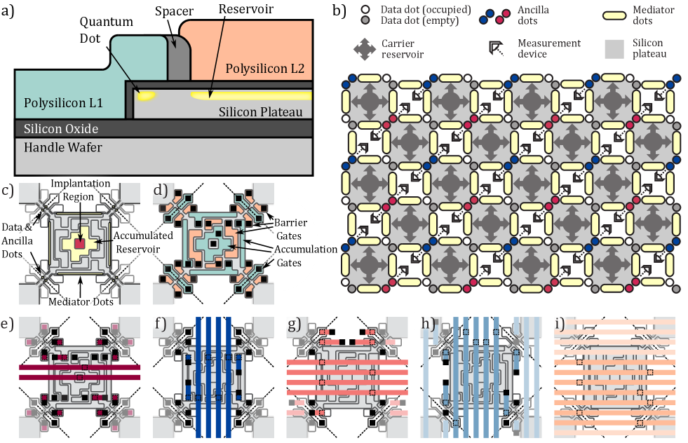
Each hardware unit cell is constructed around a single silicon plateau which facilitates the formation of quantum dot structures along the plateau boundary while also hosting standard techniques seen in planar device formation in locations away from the boundary as shown in Fig. 1a). These include the formation of implantation regions and carrier reservoirs, tunnel barriers and quantum dots. The quantum dots formed at the plateau boundary take advantage of the electric field concentration in the cross-sectional corner due to the overlapping gate electrode, resulting in strong carrier confinement Voisin et al. (2014); Corna et al. (2018). The length of the gate in the overlapped region acts to confine the quantum dot in the remaining dimension.
A recent scaled architecture proposal Cai et al. (2019) illustrated several advantages of how the integration of a spinless mediator quantum dot Srinivasa et al. (2015); Malinowski et al. (2019) connected to a charge reservoir could facilitate robustness against certain types of leakage errors in the form of physical charge movement, which would otherwise be highly detrimental to a schemes based on repeated execution of stabilizer cycles. A blueprint for a scaled quantum machine utilising the edge-dot approach, producing a 2D array of qubits interconnected via mediator dots, is illustrated in Fig. 1b).
A more detailed picture of the primitive hardware unit cell for this scaled quantum machine is shown in Fig. 1c-i), including the Front End of Line (FEOL) consisting of the physical qubit layer and supporting hardware defined by the silicon plateau, and Back End of Line (BEOL) consisting of routing metal layers for control. Each corner of the plateau is connected to a neighbouring plateau (the next adjacent hardware cell) via a shared nanowire with patterned split-gate elements acting to form a double quantum dot site. These quantum dots can be populated with charge carriers from the reservoir via the mediator quantum dots Cai et al. (2019), and act to house the physical qubits upon which the computations and error correction codes are performed. The charge reservoir consists of an ohmic implantation site illustrated in Fig. 1c) as an exposed central region of the plateau which is directly contacted by a metallic via (black squares in Fig.1d-h). The planar surface of this silicon plateau is further utilised to distribute charge from this central reservoir to each edge through a metallic accumulation gate patterned in polycrystalline silicon (poly-silicon) Layer 1 in Fig. 1d). Tunnel barriers between the accumulated reservoirs and the edge defined quantum dots can be formed either though engineered gaps Rochette et al. (2019); Hutin et al. (2019a) or dedicated barrier gates Yang et al. (2013); Zajac et al. (2018) seen patterned in poly-silicon Layer 2 in Fig. 1d). The plateau edges are overlapped with gate electrodes in poly-silicon Layer 1 which act to confine elongated quantum dots through the concentration of electric fields in the gate-edge overlap region. The plateaus are interconnected at the corners by a narrow silicon channel, commonly referred to as a “nanowire”, where split-gate technology Dupont-Ferrier et al. (2013) is used to form a double quantum dot via features in poly-silicon Layer 1 and tunable tunnel barriers via electrodes in poly-silicon Layer 2. The tunnel barriers are utilised to interface quantum structures formed in the nanowires with those formed at the edges of connected plateaus. For the long plateau edges, a mediator quantum dot is formed Malinowski et al. (2019), which serves to transfer qubit information between the quantum dots at each endpoint Srinivasa et al. (2015); Cai et al. (2019). The mediator dots have the additional advantage of introducing a means through which quantum information processing hardware elements can be physically separated to allow for efficient signal routing and integration of control or sensing peripherals required at the intra-hardware-cell level. In the example illustrated, the mediator dot is required to be the pitch of the BEOL metal routing, allowing for inter-cell connective routing of the FEOL elements as well as routing between metal layers. Space in the FEOL for integrated peripheral hardware can be seen as the (empty) regions between plateaus (grey), amounting to an area approximately equivalent to the plateaus. A diagram illustrating interconnected plateaus is provided in Supplementary Fig. S1.
II Silicon Qubit Initialisation, Readout and Control
For the execution of the surface code cycle, as detailed in § III, two varieties of qubit are utilised simultaneously; single electron spin qubits for data qubits and singlet-triplet qubits for ancillas ( and syndromes). For the control of single electron spins, electron spin resonance (ESR) methods have recently shown control fidelities of up to utilising optimised pulse schemes Yang et al. (2019) operating over µs timescales. As shown in later sections, pulse optimisation schemes such as these transfer well to globally applied spin manipulation.
For readout, the effect of Pauli spin blockade on interdot tunnelling Ono et al. (2002); Petta et al. (2005) enables in-situ double-dot readout for the syndrome qubit state, with high fidelity single-shot Pauli spin blockade detected in several implementations of silicon MOS quantum devices Harvey-Collard et al. (2018); Urdampilleta et al. (2019); Zhao et al. (2019). This readout method, combined with gate-based reflectometry measurement techniques Urdampilleta et al. (2019); West et al. (2019); Ibberson et al. (2021) results in a scalable approach to rapidly reading qubit states without the need for integrating additional charge-sensing hardware infrastructure within the FEOL. Some examples in silicon devices have shown readout fidelity of in 300 ns Ibberson et al. (2021), with others showing extrapolations to fidelity achievable in comparable timescales to the single spin qubit gates Zheng et al. (2019).
For initialisation, the triplet lifetimes within the spin blockade region is seen to vary based on species, from 200 µs for and up to 5 ms for polarised triplets West et al. (2019); Seedhouse et al. (2021), however for initialisation of the singlet state, this triplet lifetime can potentially be reduced through the use of relaxation hot-spots Srinivasa et al. (2013); Huang et al. (2019), particularly the spin-orbit driven anti-crossings found either side of the primary singlet anti-crossing, or through selective tunneling with nearby reservoirs Maune et al. (2012); Jock et al. (2022).
For two-qubit gates, the nearest-neighbour exchange interaction has lead to several realisations Veldhorst et al. (2015); Watson et al. (2018); He et al. (2019); Zajac et al. (2018); Huang et al. (2019); Sigillito et al. (2019), resulting in scaling proposals based on densely-packed two-dimensional arrays of quantum dots Veldhorst et al. (2017); Li et al. (2018), or protocols involving the transport of qubits along long chains of dots Boter et al. (2019). Other solutions such as photon-mediated two qubit interactions are accessible through hybrid material platforms Borjans et al. (2020); Clerk et al. (2020).
Alternative methods which maintain compatibility with the materials and processes used in the silicon device industry is to mediate a next-nearest-neighbour exchange through empty Baart et al. (2017), or multi-electron dots Malinowski et al. (2019). The mediating structures focused upon here take the form of elongated quantum dots which have nearest-neighbour exchange coupling between itself and a quantum dot at each endpoint (see Fig. 1b,c). This elongated quantum dot does not contain any quantum information and only acts to mediate a next-nearest-neighbour interaction between the two sites at each endpoint through the Ruderman-Kittel-Kasuya-Yosida exchange interactions Srinivasa et al. (2015). For a multielectron dot occupied by the first two electrons (or equivalent S=0 ground-state), the exchange energy between a data (D) dot and ancilla (A) dot, through the mediator (M), is approximated by Srinivasa et al. (2015); Cai et al. (2019)
| (1) |
where () is the tunnel coupling between the data-mediator (ancilla-mediator) dots, is the excited state energy on the mediator with () the energy detuning of the data (ancilla) dot from the mediator excited state. A final element required for this scheme is coherent shuttling of a single electron spin qubit between double-dot locations. Shuttling has been shown to have negligible effect on spin projection, with a recent study showing spin polarization is maintained when shuttling between two sites with a fidelity of , with for phase coherence Yoneda et al. (2021). Further, accurate charge shuttling across arrays of up to 9 dots Mills et al. (2019), and relative shuttling uncertainties below 50 parts per million Rossi et al. (2014) have also been demonstrated.
III Surface Code Unit Cell
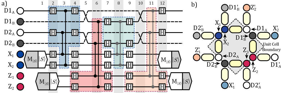
The algorithic unit cell representing the suface code is illustrated in Figure 2a), executing an interleaved XXXX and ZZZZ stabilizer. Utilizing strategic timing for state preparation and measurement of syndromes, the code cycle can be made compatible with the “tick-tock” method of executing algorithms using globally applied single qubit Hadamard gates and selective CZ gates Jones et al. (2018). The effective CNOT operations are highlighted by coloured grouping of Hadamard and CZ gates in Fig. 2a). The use of globally applied single qubit operations results in all unit cells within the quantum machine being controlled by the same input ESR signal. The approach requires embedding the quantum machine within a large peripheral 3D cavity, and the feasibility considerations for this solution is discussed in § IV. The schematic of a single edge-dot hardware cell capable of executing this stabilizer code is illustrated Fig. 2b). To execute the error correction process across the surface of the quantum machine, the unit cell must be interconnected to adjacent cells. This is achieved by positioning the ancillar and data quantum dots on the unit cell boundary, while the mediator dots (which result in the CZ operations between qubit locations), are enclosed within a cell boundary. The inter-cell operations are shown as the grey CZ connections within the surface code protocol in Fig. 2a), executed through the mediators external to the hardware cell boundary in Fig. 2b) where the equivalent dot positions in adjacent cells are indicated by a prime notation (e.g. ).
Much like the primitive cell of a crystal lattice structure, where elements are shared when located at a vertex, edge or face, the unit cell here contains on average 4 dots and (for this implementation) 3 spin 1/2 particles attributed to qubits, plus an additional 4 mediator dots. The two data qubits D1 and D2 bounding the cells consist of a single spin 1/2 particle, each contained within one of two possible quantum dots or . During the execution of the code cycle, the data spin qubit is shuttled between the dots and in order to access and complete all necessary operations between ancillas. In Fig. 2, dot locations D1A,B and D2A,B are illustrated, with the physical spin qubits indicated in Fig. 2a) as the solid traces while the empty occupancy of dots are denoted by the dashed traces.
A detailed breakdown of the 12 individual time steps within the surface code cycle seen in Fig. 2a) is presented in Supplementary Note S1. The use of singlet-triplet based syndrome qubits is compatible with the global ESR schemes as the singlet and triplets remain within their spin manifolds under global rotations. This gives rise to additional simplifications to the above protocol, however these have been omitted from the figures for clarity. For example, the initialisation and measurement process for the two ancillas could be spread over all time steps outside the two-qubit CZ operations (i.e inclusive of 9-2 for and 12-5 for ), which could facilitate additional time in the measurement and initialisation phases without extending the total time required for the code-cycle.
IV Global control of spins using a cavity peripheral
It is asserted that universally applied, or “global”, signals acting as a control input for all qubits across all cells is a desirable property for this approach to scaled quantum systems. Several proposals have also highlighted the potential use of globally applied AC fields for scaled systems of spin qubits, controlling either the entire ensemble of qubits Vandersypen et al. (2017), or sub-ensembles Veldhorst et al. (2017); Li et al. (2018). One approach to achieving this is to embed the silicon devices within a microwave cavity Vahapoglu et al. (2021). Here, the feasibility of achieving sufficiently uniform global control on the ensemble of single qubit spins within the silicon quantum dot array is discussed.
For electron spins in silicon, the spin-orbit interaction is weak when compared to other semiconductors, but still remains appreciable. The surface-roughness of the Si/SiOx interface is predicted to result in an uncontrollable distribution in the Landé -factor of up to Ferdous et al. (2018). It has been shown that this value is tunable based on changes in the electrostatic field environment Veldhorst et al. (2014); Hwang et al. (2017); Jock et al. (2018), however this degree of the Stark shift seen experimentally remains Veldhorst et al. (2015); Hwang et al. (2017). Thus, for a quantum device operating at appreciable applied magnetic field (BT), the Stark shift of the electron -factor can act as a potential source of local tunability, but cannot compensate for the entire distribution. Therefore, the quantum machine must operate within the limits of broadband microwave pulsing techniques, requiring fields substantially lower than 1T Vandersypen et al. (2017); Li et al. (2018) or otherwise operate with composite pulsing schemes requiring a train of pulses Vandersypen and Chuang (2005). For this proposal, high B0 fields are necessary for the implementation of the charge leakage protection schemes Cai et al. (2019), however pulse trains that are substantially longer than the single qubit -rotation time are an undesirable solution as they can absorb significant fractions of the coherence time budget for active qubits. As a compromise, amplitude modulation (AM) techniques can be integrated into the control.
For a quantum gate applied via a resonant microwave AC driving field, it is convenient to define the control signals and as the in-phase and quadrature components of an envelope function with carrier frequency Yang et al. (2019). This carrier is typically set by the Larmor frequency of the individual electron -factor , here it is set by the mean of the distribution. In this rotating frame, the qubit control Hamiltonian appears as
| (2) |
where are the Pauli matrices, and represents the frequency detuning of any single qubit from the mean of the distribution. Amplitude modulation can be employed as a method to expand the number of resonant peaks in the frequency domain from a single peak at , to multiple sets of side-bands that are frequency-shifted copies of the pulse envelope set by and . An amplitude modulation scheme which can be utilised to increase the number of resonant peaks output by the cavity from a single peak, to peaks separated by frequency and centred at is detailed further in Supplementary Note S2. Thus, the Stark shift can operate such that for the qubit Hamiltonian in Eq. (2) by tuning the resonant frequency of each electron to the nearest side-band within the set for (odd ) or (even ). It is expected that is required to span the frequency bandwidth created by the range of -factor distribution , given a stark shift range of .
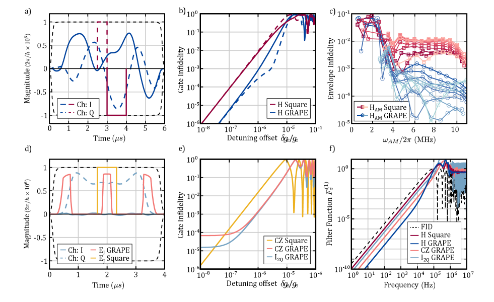
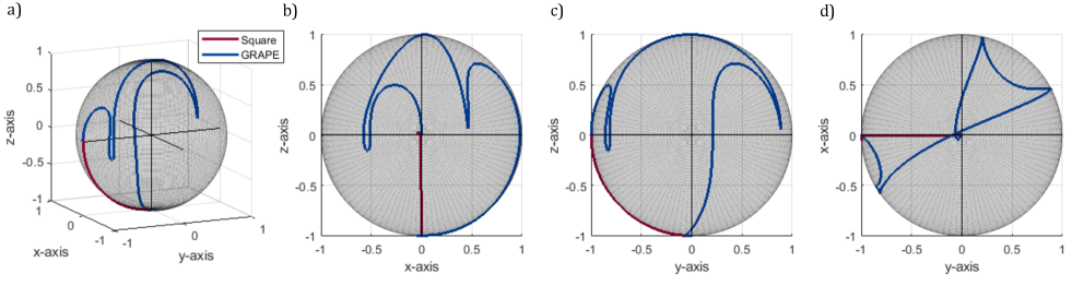
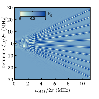
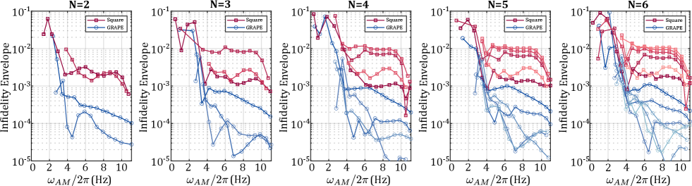
Recent studies have shown how Gradient Ascent Pulse Engineering (GRAPE) techniques Khaneja et al. (2005); De Fouquieres et al. (2011) have been utilised to design broadband pusles that can account for local environmental noise, pushing single qubit control fidelity to the limit of incoherence Yang et al. (2019). For systems in which individual qubit tunability is necessary for the uniformity of global control signals across a large array of qubits, these GRAPE methods can also be viewed as a scheme for mitigating errors in qubit tuning. Figure 3a) shows a GRAPE solution for the and envelopes required to produce a Hadamard gate, delivering a high fidelity operation over a larger bandwidth for robustness against tuning errors or small drifts in . The offset error in the tuning via the Stark shift which the gate can tolerate for given target fidelity can be seen in Fig. 3b). The solution results in a more complex trajectory over the Bloch sphere as seen in Supplementary Figure S2, requiring 6 the time of a rotation produced by a square pulse with the same amplitude limits (set as a 1 µs square pulse rotation at T). The resulting GRAPE pulse has better performance against low frequency noise coupled via the term in Eq. (2) as illustrated by the first order filter transfer function in detuning Green et al. (2013) as seen in Fig. 3f). Similar to the methods in Ref. Yang et al. (2019), the operation is trained against realistic qubit environmental noise Chan et al. (2018). While GRAPE methods can result in frequency-broadened qubit drive-lines offering a robustness to tuning errors, combining this with amplitude modulation results in the presence of multiple broadened side-bands that can also interfere with each-other. The infidelity of N=10 simultaneously driven peaks as a function of modulation frequency is seen in Figure 3c), showing disruptive levels interference between side-bands under small peak separations, however a much smaller separation in is seen to be required by a solution utilising GRAPE when compared to the square pulse solution. Figure S3 illustrates the full infidelity-envelope for the amplitude modulation method described in Eq. (S1), where N=10 peaks are simultaneously produced. A limit of MHz is observed to gain a region of Hadamard infidelity corresponding to a -factor tunability range of to move between two neighbouring peaks, or equivalently mV utilising motivated from Ref. Veldhorst et al. (2015); Hwang et al. (2017). The requirement on the Stark shift of falls within the expected range of , although this threshold could be improved through more advanced optimisation acting to reduce the cross-talk.
Pulse engineering methods can also be utilised for two-qubit gates Ball et al. (2021), where the globally applied ESR field can assist in decoupling action from local qubit noise. The mediated exchange energy in Eq. (1) can be incorporated as a voltage controlled signal in the following two qubit Hamiltonian:
| (3) |
where is the identity matrix in the single qubit subspace and represents the Kronecker product. The component of the Hamiltonian in Eq. (3) responsible for interaction between spins is valid for , Meunier et al. (2011) and has been demonstrated to produce effective CZ operations Veldhorst et al. (2015); Watson et al. (2018). The pulse shapes in Fig. 3d have been designed such that when is applied with global and signals, the resulting operation is a decoupled CZ operation. In contrast, when is not applied, i.e. for , the global and signals result instead in a decoupling identity gate applied to both independent spins. The infidelity of the decoupled CZ and Identity gates as a function of qubit detunings or (referred to a single electron offset) is shown in Fig. 3e). The GRAPE solution is contrasted against a simple square pulse in , showing improved robustness against tuning errors up to fidelity targets of , which is above the threshold for a surface code implementation Fowler et al. (2012). The resulting 1Q and 2Q GRAPE pulses also have improved performance against low frequency noise coupled via the terms in Eq. (2) and Eq. (3) compared to Square-pulse implementations, as illustrated by the first order filter transfer function in detuning Green et al. (2013); Ball et al. (2021) as seen in Fig. 3f).
V Integrated Qubit trimming circuitry
The introduction of the Stark shift as a means of tuning individual spins to a nearby resonance peak gains the ability to perform global qubit control. However this approach results in the transformation of the problem from simultaneously controlling an ensemble of qubit frequencies into one of requiring to provide as many tuned voltage references as there are qubits in the quantum machine. In effect, transferring the scaling problem from a “frequency crowding” problem into a “signal bottleneck” problem Franke et al. (2019).
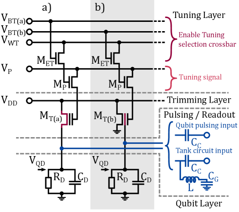
In order to achieve complete uniformity across all unit cells, the device variation must be addressable at the intra-cell level, resulting in a need for the integration of circuitry fit to address this variation. Here, the additional integrated circuitry is referred to as a “trimmer” circuit and is proposed to consist of a flash-memory-like device. Such a solution can take advantage of desirable characteristics including long-term stability and non-volatility of these integrated circuit elements, to retain voltage set-points over the lifetime of the quantum machine Hasler et al. (2021). Figure 4 illustrates a circuit schematic diagram showing two potential methods for the working principles of the trimming circuit; Fig. 4a) which operates as a source follower (buffer circuit) configuration through reduction of the single setpoint voltage through resistive division and Fig. 4b) which operates through supplying the stored potential as a direct reference for the quantum device. The resistive element within the equivalent circuit of a single quantum dot, is produced by the cumulative gate leakage to ground present in CMOS processes Schaal et al. (2018). The circuit elements shown in Figure 4 are central to performing the trimming, possessing salient characteristics similar to that of a floating-gate MOSFET including a tunable threshold voltage and non-volatility.
By trimming the threshold voltage of the device, the channel resistance in deep sub-threshold operation of the device in Fig. 4a) can become comparable to , resulting in an active voltage division which reduces the value of down to some desired value (which is presumed in this instance to target a qubit resonance line though the Stark shift discussed in § IV). A more detailed feasibility study of this resistive trimmer configuration is presented in Supplementary Note S3. The threshold voltage is tuned through charge storage within the device, converted to a voltage through the capacitance relationship. For in Fig. 4b), the stored charge within the device can be more directly converted into a voltage reference in a similar fashion to a previous proposal utilising dynamic random access memory (DRAM) Veldhorst et al. (2017). Here, the voltage reference is delivered directly to the quantum device through a direct connection between the gate electrode defining the quantum dot and the charge storage element within the memory component . For the solution shown in Figure 4, three additional MOS devices must be integrated for each trimmed object within the unit cell. A cross-bar addressing scheme is utilised for individual trimming devices across the unit cell, which becomes active during a pre-computation tuning phase for the quantum machine. The threshold voltage is selectively tuned through signal input which is connected, through activated , to the trimming devices. Word-line and bit-line voltage and combine through tuning-enable transistors , activating a selected . Based on the hardware unit cell architecture discussed in § I, the elongated mediator dots which interconnect data and ancilla qubits allow for a certain amount of physical space Cai et al. (2019) in-between the silicon plateaus where these devices can be laid out in the FEOL layer, avoiding vertical circuit integration in the form of stacking control transistor layers above the the quantum FEOL Veldhorst et al. (2017). The characteristic of non-volatility assumes operation within a consistent thermal environment and is deliverable by standard MOS memory hardware Hasler et al. (2021). This is essential for the device as, after tuning each device to the desired set-point, the selector crossbar-architecture as shown in Fig. 4 becomes idle, allowing the circuitry to be powered down more completely, reducing latent power consumption or heat load. Stability characteristics of the device must be such that the set memory state does not drift appreciably over time, as this would contribute to errors in . In this instance the stability requirements are defined by the high-fidelity region of the broadband pulses discussed in § IV.
Discussion
Here, a solution is proposed to manage resources at the quantum-classical interface within a scaled processor through integration of MOS structures at the FEOL quantum hardware level. The additional hardware is required to combat device-to-device variation which is a principle challenge when scaling quantum machines Laucht et al. (2021). The different aspect ratio between the qubit layer and the data processing layers can also complicate this quantum-classical interface Veldhorst et al. (2017), which can be avoided through the use of elongated mediator dots Cai et al. (2019) or shutting qubits through 1D dot chains Boter et al. (2019), as well as de-embedding single qubit control to be executed globally via a 3D microwave cavity Vahapoglu et al. (2021). This scaled quantum machine can be achieved through the hybridisation of SOI nanowire technologies Hutin et al. (2019a) with planar quantum dot structures Yang et al. (2013), producing an “edge dot” platform where the quantum dots are defined at the geometric boundary of a raised silicon plateau.
The hardware cell presented here is also extremely flexible, with the capacity to be re-configured to operate the surface code for different control schemes. For example, forgoing globally applied ESR of electron spins in the pursuit of an all-electrical control scheme can still utilise this same hardware architecture, with the addition of integrated micromagnet arrays Singh et al. (2020) into the FEOL. This approach can potentially utilise the space outside the plateau in each alternating cell to incorporate diagonally aligned micromagnets between the data qubit locations. This produces an engineered magnetic field gradient across each data-qubit double-dot, which can facilitate single qubit rotations Pioro-Ladriere et al. (2008). In combination with the capability of tuning the stark shift via the trimming circuit, the amplitude modulation scheme presented here is also directly transferable to a globally applied EDSR control signal for this implementation.
The type of qubits used in this hardware is also flexibly defined, based on the configuration and number of charges within each double-dot site. It is shown here that this architecture can facilitate a co-existing combination of single-electron spin qubits and two-electron Singlet-T0 Triplet qubits. A similar micromagnet configuration as the one discussed above could also be utilised for an all-electrical control implementation with both data and syndrome qubits defined in the singlet-triplet basis Wu et al. (2014). However, it is noted that approaches involving micromagnets can constitute a deviation from the materials used in the CMOS industry. Without the integrated micromagnet array, all-electrical control can still be achieved in silicon via several implementations. Single-hole spins with EDSR control Maurand et al. (2016) leverage higher spin-orbit couplings compared to electrons and singlet-triplet qubits can rely on the naturally present spin-orbit coupling for single qubit rotations Jock et al. (2018, 2022). Other all-electrical qubit species involve a (2,1) electron occupancy for the hybrid qubit implementation Shi et al. (2012) and (1,0) occupancy for qubits defined in the charge basis Hayashi et al. (2003). Note that for each of these qubit implementations listed above, tailored control schemes implementing the achievable gate-sets for these qubit varieties must be devised and are considered out of the current scope of this study.
A unit cell approach to constructing scalable quantum information processors benefits from a drasitic reduction in input overheads due to high levels of parallelisation between each cell. These hardware-based unit cells can also strongly compliment the tile-like nature of many error correction codes applied to 2D lattices of qubits. In order to successfully carry out this goal, it is necessary to tailor the design and execution towards the use of global signal control strategies such as noise-robust pulses and parallelisation schemes. From the hardware perspective, this also requires the integration of robustness against inter-cell device variations. For any scaled qubit implementation, the variation in qubit control parameters must be overcome. In the case of single electron spin qubits, utilising a 3D cavity as a control peripheral Vahapoglu et al. (2021) in which the silicon chip is embedded allows for many qubit to be addressed across a large spatial range. However, contemporary results in planar MOS devices show the expected distribution in the electron -factor Ferdous et al. (2018) far exceeds the range available through Stark-shift tunability Veldhorst et al. (2015); Hwang et al. (2017); Huang et al. (2019). Thus, the concept of tuning via stark shifts must be augmented when operating at appreciable magnetic fields for global operations to be applied to the spin ensemble. Here, the solution presented involves the use of amplitude modulation for the production of discrete side-bands, with the Stark-shift providing individual -factor tuning towards the nearest band. This approach is subject to a trade-off between the separation between the side-bands given a certain tunable range in -factor, and the cross-talk between side-bands observed at small separations. As shown here, the same engineered pulses which increase robustness against small tuning deviations in the -factor can also result in reduced cross-talk between side-bands compared to equivalent square-pulse implementations. With the added design element of intentionally reducing cross-talk between side-bands within the optimisation process, this trade-off between cross-talk and Stark-shift could be further improved. The signals executing the CZ operation can also be made compatible with global control operations through the electrical tuning of the exchange energy between features in the unit cell. Tuning the Stark shift will result in alterations to the terms in Eq. (1), however by tuning of the potential on the barrier gates situated between the Dots and the Mediators in Fig. 2b) can compensate via directly tuning the ratio, ensuring uniformity in across all sites. The magnitude of can then be modulated through signal applied to the Mediator accumulation gate, which has a linear relationship to both and , resulting in
For the global control solutions presented here, the surface code cycle is executed within µs (), assuming near-negligible electron shuttling times Yoneda et al. (2021). This is well below the state-of-the-art single-spin coherence time of ms Yang et al. (2019) as derived from a Randomized Benchmarking experiment utilising GRAPE pulses. The collective ancilla qubit measurement and initialisation time for this protocol is 12-28 µs depending on the implementation. Current measurements in silicon nanowires have lead to the determination of a PSB signal with 99% fidelity within 5.6 µs Oakes et al. (2022), leaving approximately a 6-22 µs budget for -state initialisation via mediator/reservoirs in the first instance. This time budget can also be extended over multiple code-cycles if necessary, through adopting plaquette sequencing protocols discussed in Ref. Cai et al. (2019).
Focusing on the mature CMOS industry for the development of quantum processors has the core benefit of being able to draw upon many different advancements and techniques for information processing and storage Gonzalez-Zalba et al. (2021). A similar approach for addressing device variation includes embedding a quantum machine into a DRAM-style circuit Veldhorst et al. (2017), where the 6T3C/dot cell stores a pre-tuned voltage supplied from a variable source on a capacitor near each quantum dot, and refreshed over a cyclic period. For this approach, the hold-capacitor must be large enough for a sufficiently stable voltage (and thus resonant frequency via the Stark shift in the -factor) for high fidelity qubit operations. Conversely, this capacitive element must also be small enough not to dominate the integrated dispersive readout signals Schaal et al. (2019). In contrast, the method presented here proposes the specific integration of non-volatile memory elements for the storage of these pre-tuned voltage settings. These voltage references are continually applied by the non-volatile elements and are therefore not subject to the same limitations set by capacitive decay constants or cycle-to-cycle variations, but will still be limited by Johnson noise generated by the voltage reference elements in a similar way. Both approaches, however, require a potentially high set-up cost represented by a pre-computation trimming phase which identifies the correct operating conditions for each qubit element, however an advantage for the implementation presented here is that this tuning circuitry has the option to become dormant during computation phases due to the non-volatility of the integrated memory elements, potentially reducing the latent power consumption of the device.
With the addition of trimming internal to the hardware unit cell, the number of inputs required to set the state of the quantum machine can be drastically reduced through the interconnection of cells. This results in a hardware in which the number of inputs scales with the complexity of the unit cell, rather than the number of unit cells required to produce the quantum machine Franke et al. (2019), ensuring the extensibility of the qubit platform. The physical layout of the CMOS elements in the FEOL, and the routing between the elements at the quantum-classical interface, is considered to be out of scope for this initial work, however for the solution presented in § V, 48 elements are required per unit cell to connect 16 structures which require trimming (the reservoir accumulation gate, and barriers between the mediators and reservoir are discounted here, as these do not require precise tuning to function). As the area between silicon plateaus is for the direct routing solution presented in Fig. 2, where is the BEOL routing pitch, this affords an area budget of per control element before the size of these elements impacts the length of the mediator dots which are in this example. A potential alternative method for spin transfer would be to replace the mediator with a spin-shuttling chain of quantum dots, which has been studied elsewhere Boter et al. (2019), and has different trade-offs regarding increased numbers of electrodes and control signals.
While the extension of this architecture towards lattice surgery methods is also considered out of the scope for a study of the individual hardware cell, it is noted that a deviation from globally applied electrical control signals towards grouping regions of the surface into distinct areas, perhaps governed by separate DACs, can facilitate lattice splitting and merging required for lattice surgery Horsman et al. (2012). For example, inactivity of CZ mediator signals along a selected row/column results in dormant regions in the surface structure, producing a split between two distinct regions. Further, it is also feasible to have intermittently placed, dedicated control circuitry offsetting entire regions of quantum unit cells in the FEOL, as the surface code has been shown to be robust against both time-resolved, and/or spatial interruptions defects Strikis et al. (2021). The exact geometric topology and layout of the quantum VS classical regions in the expanded FEOL is considered to be beyond the scope of the unit cell as studied here.
Conclusion
Defining a hardware unit cell which is complimentary to a specific stabiliser code cycle can lead to a highly parallelised approach to the execution of large scale quantum information processing. Here, a case study is presented which utilises a hybrid between two prevalent silicon MOS technologies, combining the advantages of current state-of-the-art solid-state quantum hardware approaches with memory storage techniques. The choice of design to include integrated mediator quantum dots makes the stored quantum information additionally robust against leakage error types which cannot be protected against through standard quantum error detection protocols. The adapted code-cycle presented here allows for the implementation of globally applied single-qubit rotations across the entire ensemble of qubit resonant frequencies, as well as selectively applied two-qubit CZ operations from a global signal source. The inclusion of non-volatile memory elements within the hardware unit cell also reduces the signal overheads to expand with the unit cell size rather than with the number of cells. The result is a complete unit cell approach to constructing a robust quantum information processing machine of arbitrary scale in silicon.
Acknowledgments
The author would like to thank J. J. L. Morton, M. F. Gonzalez-Zalba, S. C. Benjamin and Z. Cai for valuable discussions and comments on the manuscript
Author Information
The Author is supported by Quantum Motion, a start-up developing silicon-based quantum computing.
References
- Terhal (2015) B. M. Terhal, “Quantum error correction for quantum memories,” Reviews of Modern Physics 87, 307 (2015).
- O’Gorman and Campbell (2017) J. O’Gorman and E. T. Campbell, “Quantum computation with realistic magic-state factories,” Physical Review A 95, 032338 (2017).
- Hutin et al. (2019a) L. Hutin, B. Bertrand, Y.-M. Niquet, J.-M. Hartmann, M. Sanquer, S. De Franceschi, T. Meunier, and M. Vinet, “Soi mos technology for spin qubits,” ECS Transactions 93, 35 (2019a).
- Li et al. (2020) R. Li, N. I. D. Stuyck, S. Kubicek, J. Jussot, B. T. Chan, F. A. Mohiyaddin, A. Elsayed, M. Shehata, G. Simion, C. Godfrin, Y. Canvel, T. Ivanov, L. Goux, B. Govoreanu, and I. P. Radu, “A flexible 300 mm integrated si mos platform for electron-and hole-spin qubits exploration,” (IEEE, 2020) pp. 38.3.1–38.3.4.
- Zwerver et al. (2022) A. M. J. Zwerver, T. Krähenmann, T. F. Watson, L. Lampert, H. C. George, R. Pillarisetty, S. A. Bojarski, P. Amin, S. V. Amitonov, J. M. Boter, R. Caudillo, D. Corras-Serrano, J. P. Dehollain, G. Droulers, E. M. Henry, R. Kotlyar, M. Lodari, F. Luthi, D. J. Michalak, B. K. Mueller, S. Neyens, J. Roberts, N. Samkharadze, G. Zheng, G. Zietz, O. K. Scappucci, M. Veldhorst, L. M. K. Vandersypen, and J. S. Clarke, “Qubits made by advanced semiconductor manufacturing,” Nature Electronics 5, 184–190 (2022).
- Vandersypen et al. (2017) L. M. K. Vandersypen, H. Bluhm, J. S. Clarke, A. S. Dzurak, R. Ishihara, A. Morello, D. J. Reilly, L. R. Schreiber, and M. Veldhorst, “Interfacing spin qubits in quantum dots and donors—hot, dense, and coherent,” npj Quantum Information 3, 1–10 (2017).
- Gonzalez-Zalba et al. (2021) M. F. Gonzalez-Zalba, S. de Franceschi, E. Charbon, T. Meunier, M. Vinet, and A. S. Dzurak, “Scaling silicon-based quantum computing using cmos technology: State-of-the-art, challenges and perspectives,” Nature Electronics 4, 872–884 (2021).
- Pauka et al. (2021) S. J. Pauka, K. Das, R. Kalra, A. Moini, Y. Yang, M. Trainer, A. Bousquet, C. Cantaloube, N. Dick, G. C. Gardner, M. J. Manfra, and D. J. Reilly, “A cryogenic cmos chip for generating control signals for multiple qubits,” Nature Electronics 4, 64–70 (2021).
- Veldhorst et al. (2017) M. Veldhorst, H. G. J. Eenink, C.-H. Yang, and A. S. Dzurak, “Silicon cmos architecture for a spin-based quantum computer,” Nature communications 8, 1–8 (2017).
- Li et al. (2018) R. Li, L. Petit, D. P. Franke, J. P. Dehollain, J. Helsen, M. Steudtner, N. K. Thomas, Z. R. Yoscovits, K. J. Singh, S. Wehner, L. M. K. Vandersypen, J. S. Clarke, and M. Veldhorst, “A crossbar network for silicon quantum dot qubits,” Science advances 4, eaar3960 (2018).
- Hollenberg et al. (2006) L. C. L. Hollenberg, A. D. Greentree, A. G. Fowler, and C. J. Wellard, “Two-dimensional architectures for donor-based quantum computing,” Physical Review B 74, 045311 (2006).
- Pica et al. (2016) G. Pica, B. W. Lovett, R. N. Bhatt, T. Schenkel, and S. A. Lyon, “Surface code architecture for donors and dots in silicon with imprecise and nonuniform qubit couplings,” Physical Review B 93, 035306 (2016).
- Tosi et al. (2017) G. Tosi, F. A. Mohiyaddin, V. Schmitt, S. Tenberg, R. Rahman, G. Klimeck, and A. Morello, “Silicon quantum processor with robust long-distance qubit couplings,” Nature communications 8, 1–11 (2017).
- Voisin et al. (2014) B. Voisin, V.-H. Nguyen, J. Renard, X. Jehl, S. Barraud, F. Triozon, M. Vinet, I. Duchemin, Y.-M. Niquet, S. De Franceschi, and M. Sanquer, “Few-electron edge-state quantum dots in a silicon nanowire field-effect transistor,” Nano letters 14, 2094–2098 (2014).
- Dupont-Ferrier et al. (2013) E. Dupont-Ferrier, B. Roche, B. Voisin, X. Jehl, R. Wacquez, M. Vinet, M. Sanquer, and S. De Franceschi, “Coherent coupling of two dopants in a silicon nanowire probed by landau-zener-stückelberg interferometry,” Physical review letters 110, 136802 (2013).
- Hutin et al. (2019b) L. Hutin, B. Bertrand, E. Chanrion, H. Bohuslavskyi, F. Ansaloni, T.-Y. Yang, J. Michniewicz, D. J. Niegemann, C. Spence, T. Lundberg, A. Chatterjee, A. Crippa, J. Li, R. Maurand, X. Jehl, M. Sanquer, M. F. Gonzalez-Zalba, F. Kuemmeth, Y.-M. Niquet, S. De Franceschi, M. Urdampilleta, T. Meunier, and M. Vinet, “Gate reflectometry for probing charge and spin states in linear si mos split-gate arrays,” (IEEE, 2019).
- Ansaloni et al. (2020) F. Ansaloni, A. Chatterjee, H. Bohuslavskyi, B. Bertrand, L. Hutin, M. Vinet, and F. Kuemmeth, “Single-electron operations in a foundry-fabricated array of quantum dots,” Nature communications 11, 1–7 (2020).
- Chanrion et al. (2020) E. Chanrion, D. J. Niegemann, B. Bertrand, C. Spence, B. Jadot, J. Li, P.-A. Mortemousque, L. Hutin, R. Maurand, X. Jehl, M. Sanquer, S. De Franceschi, C. Bäuerle, F. Balestro, Y.-M. Niquet, M. Vinet, T. Meunier, and M. Urdampilleta, “Charge detection in an array of cmos quantum dots,” Physical Review Applied 14, 024066 (2020).
- Trifunovic et al. (2012) L. Trifunovic, O. Dial, M. Trif, J. R. Wootton, R. Abebe, A. Yacoby, and D. Loss, “Long-distance spin-spin coupling via floating gates,” Physical review X 2, 011006 (2012).
- Duan et al. (2020) J. Duan, M. A. Fogarty, J. Williams, L. Hutin, M. Vinet, and J. J. L. Morton, “Remote capacitive sensing in two-dimensional quantum-dot arrays,” Nano Letters 20, 7123–7128 (2020).
- Gilbert et al. (2020) W. Gilbert, A. Saraiva, W. H. Lim, C. H. Yang, A. Laucht, B. Bertrand, N. Rambal, L. Hutin, C. C. Escott, M. Vinet, and A. S. Dzurak, “Single-electron operation of a silicon-cmos 2 × 2 quantum dot array with integrated charge sensing,” Nano Letters 20, 7882–7888 (2020).
- Veldhorst et al. (2014) M. Veldhorst, J. C. C. Hwang, C. H. Yang, A. W. Leenstra, B. de Ronde, J. P. Dehollain, J. T. Muhonen, F. E. Hudson, K. M. Itoh, A. Morello, and A. S. Dzurak, “An addressable quantum dot qubit with fault-tolerant control-fidelity,” Nature nanotechnology 9, 981–985 (2014).
- Veldhorst et al. (2015) M. Veldhorst, C. H. Yang, J. C. C. Hwang, W. Huang, J. P. Dehollain, J. T. Muhonen, S. Simmons, A. Laucht, F. E. Hudson, K. M. Itoh, A. Morello, and A. S. Dzurak, “A two-qubit logic gate in silicon,” Nature 526, 410–414 (2015).
- Reilly (2015) D. J. Reilly, “Engineering the quantum-classical interface of solid-state qubits,” npj Quantum Inf. 1, 15011 (2015).
- Reilly (2019) D. J. Reilly, “Challenges in scaling-up the control interface of a quantum computer,” (IEEE, 2019) pp. 31.7.1–31.7.6.
- Franke et al. (2019) D. P. Franke, J. S. Clarke, L. M. K. Vandersypen, and M. Veldhorst, “Rent’s rule and extensibility in quantum computing,” Microprocessors and Microsystems 67, 1–7 (2019).
- Fowler et al. (2012) A. G. Fowler, M. Mariantoni, J. M. Martinis, and A. N. Cleland, “Surface codes: Towards practical large-scale quantum computation,” Physical Review A 86, 032324 (2012).
- Corna et al. (2018) A. Corna, L. Bourdet, R. Maurand, A. Crippa, D. Kotekar-Patil, H. Bohuslavskyi, R. Laviéville, L. Hutin, S. Barraud, X. Jehl, M. Vinet, S. De Franceschi, Y.-M. Niquet, and M. Sanquer, “Electrically driven electron spin resonance mediated by spin–valley–orbit coupling in a silicon quantum dot,” npj quantum information 4, 1–7 (2018).
- Cai et al. (2019) Z. Cai, M. A. Fogarty, S. Schaal, S. Patomäki, S. C. Benjamin, and J. J. L. Morton, “A silicon surface code architecture resilient against leakage errors,” Quantum 3, 212 (2019).
- Srinivasa et al. (2015) V. Srinivasa, H. Xu, and J. M. Taylor, “Tunable spin-qubit coupling mediated by a multielectron quantum dot,” Physical review letters 114, 226803 (2015).
- Malinowski et al. (2019) F. K. Malinowski, F. Martins, T. B. Smith, S. D. Bartlett, A. C. Doherty, P. D. Nissen, S. Fallahi, G. C. Gardner, M. J. Manfra, C. M. Marcus, and F. Kuemmeth, “Fast spin exchange across a multielectron mediator,” Nature communications 10, 1–6 (2019).
- Rochette et al. (2019) S. Rochette, M. Rudolph, A.-M. Roy, M. J. Curry, G. Ten Eyck, R. P. Manginell, J. R. Wendt, T. Pluym, S. M. Carr, D. R. Ward, M. P. Lilly, M. S. Carroll, and M. Pioro-Ladrière, “Quantum dots with split enhancement gate tunnel barrier control,” Applied Physics Letters 114, 083101 (2019).
- Yang et al. (2013) C. H. Yang, A. Rossi, R. Ruskov, N. S. Lai, F. A. Mohiyaddin, S. Lee, C. Tahan, G. Klimeck, A. Morello, and A. S. Dzurak, “Spin-valley lifetimes in a silicon quantum dot with tunable valley splitting,” Nature communications 4, 1–8 (2013).
- Zajac et al. (2018) D. M. Zajac, A. J. Sigillito, M. Russ, F. Borjans, J. M. Taylor, G. Burkard, and J. R. Petta, “Resonantly driven cnot gate for electron spins,” Science 359, 439–442 (2018).
- Jones et al. (2018) C. Jones, M. A. Fogarty, A. Morello, M. F. Gyure, A. S. Dzurak, and T. D. Ladd, “Logical qubit in a linear array of semiconductor quantum dots,” Physical Review X 8, 021058 (2018).
- Yang et al. (2019) C. H. Yang, K. W. Chan, R. Harper, W. Huang, T. Evans, J. C. C. Hwang, B. Hensen, A. Laucht, T. Tanttu, F. E. Hudson, S. T. Flammia, K. M. Itoh, A. Morello, S. D. Bartlett, and A. S. Dzurak, “Silicon qubit fidelities approaching incoherent noise limits via pulse engineering,” Nature Electronics 2, 151–158 (2019).
- Ono et al. (2002) K. Ono, D. G. Austing, Y. Tokura, and S. Tarucha, “Current rectification by pauli exclusion in a weakly coupled double quantum dot system,” Science 297, 1313–1317 (2002).
- Petta et al. (2005) J. R. Petta, A. C. Johnson, J. M. Taylor, E. A. Laird, A. Yacoby, M. D. Lukin, C. M. Marcus, M. P. Hanson, and A. C. Gossard, “Coherent manipulation of coupled electron spins in semiconductor quantum dots,” Science 309, 2180–2184 (2005).
- Harvey-Collard et al. (2018) P. Harvey-Collard, B. D’Anjou, M. Rudolph, N. T. Jacobson, J. Dominguez, G. A. Ten Eyck, J. R. Wendt, T. Pluym, M. P. Lilly, W. A. Coish, M. Pioro-Ladrière, and M. S. Carroll, “High-fidelity single-shot readout for a spin qubit via an enhanced latching mechanism,” Physical Review X 8, 021046 (2018).
- Urdampilleta et al. (2019) M. Urdampilleta, D. J. Niegemann, E. Chanrion, B. Jadot, C. Spence, P.-A. Mortemousque, C. Bäuerle, L. Hutin, B. Bertrand, S. Barraud, R. Maurand, M. Sanquer, X. Jehl, S. De Franceschi, M. Vinet, and T. Meunier, “Gate-based high fidelity spin readout in a cmos device,” Nature nanotechnology 14, 737–741 (2019).
- Zhao et al. (2019) R. Zhao, T. Tanttu, K. Y. Tan, B. Hensen, K. W. Chan, J. C. C. Hwang, R. C. C. Leon, C. H. Yang, W. Gilbert, F. E. Hudson, K. M. Itoh, A. A. Kiselev, T. D. Ladd, A. Morello, A. S. Dzurak, and A. Laucht, “Single-spin qubits in isotopically enriched silicon at low magnetic field,” Nature communications 10, 1–9 (2019).
- West et al. (2019) A. West, B. Hensen, A. Jouan, T. Tanttu, C.-H. Yang, A. Rossi, M. F. Gonzalez-Zalba, F. E. Hudson, A. Morello, D. J. Reilly, and A. S. Dzurak, “Gate-based single-shot readout of spins in silicon,” Nature nanotechnology 14, 437–441 (2019).
- Ibberson et al. (2021) D. J. Ibberson, T. Lundberg, J. A. Haigh, L. Hutin, B. Bertrand, S. Barraud, C.-M. Lee, N. A. Stelmashenko, G. A. Oakes, L. Cochrane, J. W. A. Robinson, M. Vinet, M. F. Gonzalez-Zalba, and L. A. Ibberson, “Large dispersive interaction between a cmos double quantum dot and microwave photons,” PRX Quantum 2, 020315 (2021).
- Zheng et al. (2019) G. Zheng, N. Samkharadze, M. L. Noordam, N. Kalhor, D. Brousse, A. Sammak, G. Scappucci, and L. M. K. Vandersypen, “Rapid gate-based spin read-out in silicon using an on-chip resonator,” Nature nanotechnology 14, 742–746 (2019).
- Seedhouse et al. (2021) A. E. Seedhouse, T. Tanttu, R. C. C. Leon, R. Zhao, K. Y. Tan, B. Hensen, F. E. Hudson, K. M. Itoh, J. Yoneda, C. H. Yang, A. Morello, A. Laucht, S. N. Coppersmith, A. Saraiva, and A. S. Dzurak, “Pauli blockade in silicon quantum dots with spin-orbit control,” PRX Quantum 2, 010303 (2021).
- Srinivasa et al. (2013) V. Srinivasa, K. C. Nowack, M. Shafiei, L. M. K. Vandersypen, and J. M. Taylor, “Simultaneous spin-charge relaxation in double quantum dots,” Physical review letters 110, 196803 (2013).
- Huang et al. (2019) W. Huang, C. H. Yang, K. W. Chan, T. Tanttu, B. Hensen, R. C. C. Leon, M. A. Fogarty, J. C. C. Hwang, F. E. Hudson, K. M. Itoh, A. Morello, A. Laucht, and A. S. Dzurak, “Fidelity benchmarks for two-qubit gates in silicon,” Nature 569, 532–536 (2019).
- Maune et al. (2012) B. M. Maune, M. G. Borselli, B. Huang, T. D. Ladd, P. W. Deelman, K. S. Holabird, A. A. Kiselev, I. Alvarado-Rodriguez, R. S. Ross, A. E. Schmitz, M. Sokolich, C. A. Watson, M. F. Gyure, and A. T. Hunter, “Coherent singlet-triplet oscillations in a silicon-based double quantum dot,” Nature 481, 344–347 (2012).
- Jock et al. (2022) R. M. Jock, N. T. Jacobson, M. Rudolph, D. R. Ward, M. S. Carroll, and D. R. Luhman, “A silicon singlet–triplet qubit driven by spin-valley coupling,” Nature communications 13, 1–9 (2022).
- Watson et al. (2018) T. F. Watson, S. G. J. Philips, E. Kawakami, D. R. Ward, P. Scarlino, M. Veldhorst, D. E. Savage, M. G. Lagally, M. Friesen, S. N. Coppersmith, M. A. Eriksson, and L. M. K. Vandersypen, “A programmable two-qubit quantum processor in silicon,” nature 555, 633–637 (2018).
- He et al. (2019) Y. He, S. K. Gorman, D. Keith, L. Kranz, J. G. Keizer, and M. Y. Simmons, “A two-qubit gate between phosphorus donor electrons in silicon,” Nature 571, 371–375 (2019).
- Sigillito et al. (2019) A. J. Sigillito, M. J. Gullans, L. F. Edge, M. Borselli, and J. R. Petta, “Coherent transfer of quantum information in a silicon double quantum dot using resonant swap gates,” npj Quantum Information 5, 1–7 (2019).
- Boter et al. (2019) J. M. Boter, J. P. Dehollain, J. P. G. van Dijk, T. Hensgens, R. Versluis, J. S. Clarke, M. Veldhorst, F. Sebastiano, and L. M. K. Vandersypen, “A sparse spin qubit array with integrated control electronics,” (IEEE, 2019) pp. 31–4.
- Borjans et al. (2020) F. Borjans, X. G. Croot, X. Mi, M. J. Gullans, and J. R. Petta, “Resonant microwave-mediated interactions between distant electron spins,” Nature 577, 195–198 (2020).
- Clerk et al. (2020) A. A. Clerk, K. W. Lehnert, P. Bertet, J. R. Petta, and Y. Nakamura, “Hybrid quantum systems with circuit quantum electrodynamics,” Nature Physics 16, 257–267 (2020).
- Baart et al. (2017) T. A. Baart, T. Fujita, C. Reichl, W. Wegscheider, and L. M. K. Vandersypen, “Coherent spin-exchange via a quantum mediator,” Nature nanotechnology 12, 26–30 (2017).
- Yoneda et al. (2021) J. Yoneda, W. Huang, M. Feng, C. H. Yang, K. W. Chan, T. Tanttu, W. Gilbert, R. C. C. Leon, F. E. Hudson, K. M. Itoh, A. Morello, S. D. Bartlett, A. Laucht, A. Saraiva, and A. S. Dzurak, “Coherent spin qubit transport in silicon,” Nature Communications 12, 1–9 (2021).
- Mills et al. (2019) A. R. Mills, D. M. Zajac, M. J. Gullans, F. J. Schupp, T. M. Hazard, and J. R. Petta, “Shuttling a single charge across a one-dimensional array of silicon quantum dots,” Nature communications 10, 1–6 (2019).
- Rossi et al. (2014) A. Rossi, T. Tanttu, K. Y. Tan, I. Iisakka, R. Zhao, K. W. Chan, G. C. Tettamanzi, S. Rogge, Andrew S. Dzurak, and M. Möttönen, “An accurate single-electron pump based on a highly tunable silicon quantum dot,” Nano letters 14, 3405–3411 (2014).
- Vahapoglu et al. (2021) E. Vahapoglu, J. P. Slack-Smith, R. C. C. Leon, W. H. Lim, F. E. Hudson, T. Day, T. Tanttu, C. H. Yang, A. Laucht, A. S. Dzurak, and J. J. Pla, “Single-electron spin resonance in a nanoelectronic device using a global field,” Science Advances 7, eabg9158 (2021).
- Ferdous et al. (2018) R. Ferdous, K. W. Chan, M. Veldhorst, J. C. C. Hwang, C. H. Yang, H. Sahasrabudhe, G. Klimeck, A. Morello, A. S. Dzurak, and R. Rahman, “Interface-induced spin-orbit interaction in silicon quantum dots and prospects for scalability,” Physical Review B 97, 241401 (2018).
- Hwang et al. (2017) J. C. C. Hwang, C. H. Yang, M. Veldhorst, N. Hendrickx, M. A. Fogarty, W. Huang, F. E. Hudson, A. Morello, and A. S. Dzurak, “Impact of g-factors and valleys on spin qubits in a silicon double quantum dot,” Physical Review B 96, 045302 (2017).
- Jock et al. (2018) R. M. Jock, N. T. Jacobson, P. Harvey-collard, A. M. Mounce, V. Srinivasa, D. R. Ward, J. Anderson, R. Manginell, J. R. Wendt, M. Rudolph, T. Pluym, J. K. Gamble, A. D. Baczewski, W. M. Witzel, and M. S. Carroll, “A silicon metal-oxide-semiconductor electron spin-orbit qubit,” Nature communications 9, 1–8 (2018).
- Vandersypen and Chuang (2005) L. M. K. Vandersypen and I. L. Chuang, “Nmr techniques for quantum control and computation,” Reviews of modern physics 76, 1037 (2005).
- Khaneja et al. (2005) N. Khaneja, T. Reiss, C. Kehlet, T. Schulte-Herbrüggen, and S. J. Glaser, “Optimal control of coupled spin dynamics: design of nmr pulse sequences by gradient ascent algorithms,” Journal of magnetic resonance 172, 296–305 (2005).
- De Fouquieres et al. (2011) P. De Fouquieres, S. G. Schirmer, S. J. Glaser, and I. Kuprov, “Second order gradient ascent pulse engineering,” Journal of Magnetic Resonance 212, 412–417 (2011).
- Green et al. (2013) T. J. Green, J. Sastrawan, H. Uys, and M. J. Biercuk, “Arbitrary quantum control of qubits in the presence of universal noise,” New Journal of Physics 15, 095004 (2013).
- Chan et al. (2018) K. W. Chan, W. Huang, C. H. Yang, J. C. C. Hwang, B. Hensen, T. Tanttu, F. E. Hudson, K. M. Itoh, A. Laucht, A. Morello, and A. S. Dzurak, “Assessment of a silicon quantum dot spin qubit environment via noise spectroscopy,” Physical Review Applied 10, 044017 (2018).
- Ball et al. (2021) H. Ball, M. J. Biercuk, A. R. R. Carvalho, J. Chen, M. Hush, L. A. De Castro, L. Li, P. J. Liebermann, H. J. Slatyer, C. Edmunds, V. Frey, C. Hempel, and A. Milne, “Software tools for quantum control: Improving quantum computer performance through noise and error suppression,” Quantum Science and Technology 6, 044011 (2021).
- Meunier et al. (2011) T. Meunier, V. E. Calado, and L. M. K. Vandersypen, “Efficient controlled-phase gate for single-spin qubits in quantum dots,” Physical Review B 83, 121403 (2011).
- Hasler et al. (2021) J. Hasler, N. Dick, K. Das, B. Degnans, A. Moini, and D. Reilly, “Cryogenic floating-gate cmos circuits for quantum control,” IEEE Transactions on Quantum Engineering (2021).
- Schaal et al. (2018) S. Schaal, S. Barraud, J. J. L. Morton, and M. F. Gonzalez-Zalba, “Conditional dispersive readout of a cmos single-electron memory cell,” Physical Review Applied 9, 054016 (2018).
- Laucht et al. (2021) A. Laucht, F. Hohls, N. Ubbelohde, M. F. Gonzalez-Zalba, D. J. Reilly, S. Stobbe, T. Schröder, P. Scarlino, J. V. Koski, A. Dzurak, C.-H. Yang, J. Yoneda, F. Kuemmeth, , H. Bluhm, J. Pla, C. Hill, J. Salfi, A. Oiwa, J. T. Muhonen, E. Verhagen, M. D. LaHaye, H. H. Kim, A. W. Tsen, D. Culcer, A. Geresdi, J. A. Mol, V. Mohan, P. K. Jain, and J. Baugh, “Roadmap on quantum nanotechnologies,” Nanotechnology 32, 162003 (2021).
- Singh et al. (2020) K. Singh, J. S. Clarke, M. Veldhorst, and L. M. K. Vandersypen, “Quantum dot devices,” (2020), US Patent App. 16/616,427.
- Pioro-Ladriere et al. (2008) M. Pioro-Ladriere, T. Obata, Y. Tokura, Y.-S. Shin, T. Kubo, K. Yoshida, T. Taniyama, and S. Tarucha, “Electrically driven single-electron spin resonance in a slanting zeeman field,” Nature Physics 4, 776–779 (2008).
- Wu et al. (2014) X. Wu, D. R. Ward, J. R. Prance, D. Kim, J. K. Gamble, R. T. Mohr, Z. Shi, D. E. Savage, M. G. Lagally, M. Friesen, S. N. Coppersmith, and M. A. Eriksson, “Two-axis control of a singlet–triplet qubit with an integrated micromagnet,” Proceedings of the National Academy of Sciences 111, 11938–11942 (2014).
- Maurand et al. (2016) R. Maurand, X. Jehl, D. Kotekar-Patil, A. Corna, H. Bohuslavskyi, R. Laviéville, L. Hutin, S. Barraud, M. Vinet, M. Sanquer, and S. De Franceschi, “A cmos silicon spin qubit,” Nature communications 7, 1–6 (2016).
- Shi et al. (2012) Z. Shi, C. B. Simmons, J. R. Prance, J. K. Gamble, T. S. Koh, Y.-P. Shim, X. Hu, D. E. Savage, M. G. Lagally, M. A. Eriksson, M. Friesen, and S. N. Coppersmith, “Fast hybrid silicon double-quantum-dot qubit,” Physical review letters 108, 140503 (2012).
- Hayashi et al. (2003) T. Hayashi, T. Fujisawa, H.-D. Cheong, Y. H. Jeong, and Y. Hirayama, “Coherent manipulation of electronic states in a double quantum dot,” Physical review letters 91, 226804 (2003).
- Oakes et al. (2022) G. A. Oakes, V. N. Ciriano-Tejel, D. Wise, M. A. Fogarty, T. Lundberg, C. Lainé, S. Schaal, F. Martins, D. J. Ibberson, L. Hutin, B. Bertrand, N. Stelmashenko, J. A. W. Robinson, L. Ibberson, A. Hashim, I. Siddiqi, A. Lee, M. Vinet, C. G. Smith, J. L. L. Morton, and M. F. Gonzalez-Zalba, “Fast high-fidelity single-shot readout of spins in silicon using a single-electron box,” arXiv:2203.06608 (2022).
- Schaal et al. (2019) S. Schaal, A. Rossi, T.-Y. Ciriano-Tejel, V. N .and Yang, S. Barraud, J. J. L. Morton, and M. F. Gonzalez-Zalba, “A cmos dynamic random access architecture for radio-frequency readout of quantum devices,” Nature Electronics 2, 236–242 (2019).
- Horsman et al. (2012) C. Horsman, A. G. Fowler, S. Devitt, and R. Van Meter, “Surface code quantum computing by lattice surgery,” New Journal of Physics 14, 123011 (2012).
- Strikis et al. (2021) A. Strikis, S. C. Benjamin, and B. J. Brown, “Quantum computing is scalable on a planar array of qubits with fabrication defects,” arXiv:2111.06432 (2021).
- Fujita and Amemiya (1993) O. Fujita and Y. Amemiya, “A floating-gate analog memory device for neural networks,” IEEE transactions on electron devices 40, 2029–2035 (1993).
Supplementary Figures
Supplementary Notes
S1 Time-Steps for the Surface Code
A breakdown of the individual time steps within the surface code cycle is as follows:
-
1.
Initialisation of the ancilla as a singlet . Data qubits located in D1A and D2A dots are idle. This time step is also coincident with the measurement of the ancilla from the previous cycle (grey in Fig. 2a).
-
2.
Hadamard gates applied to all active spin qubits (D1A,D2A and individual elements of ) coincident with initialisation of the ancilla as a singlet .
- 3.
-
4.
Hadamard gate globally applied to all individual spins.
-
5.
Shuttling of the data qubit form within dot location to . This constitutes a charge shuttling from one side of a nanowire to another.
-
6.
Concurrently applied CZ operations between each element of the ancilla and D1B or D2B, internal to the hardware unit cell.
-
7.
Hadamard gate applied to all spins. For the ancilla, these Hadamard operations cancel with the operations form time step 4.
-
8.
Concurrently applied CZ operations between each element of the ancilla and D1 or D2. CZ gates are external to the hardware unit cell, shown as grey in Fig. 2a).
-
9.
Hadamard gate applied to all spin qubits.
-
10.
Shuttling of the data qubit form within dot location to .
-
11.
Concurrently applied CZ operations between each element of the ancilla and D1 or D2. Gates are external to the hardware unit cell.
-
12.
Hadamard gate applied to all active spin qubits coincident with the measurement of the ancilla. The unassigned Hadamard gate applied to D1A and D2A effectively swaps and ancillas for the next cycle unless a global Hadamard is applied in step 1 of the next cycle.
S2 Amplitude Modulation Scheme
An amplitude modulation scheme which can be utilised to increase the number of resonant peaks output by the cavity from a single peak, to N peaks centred at , is given by:
| (S1) |
Here, is the modulation envelope which results in the replication of the pulse defined by and at frequency detunings separated by . For each sideband, a phase correction term is included, which is dependent upon the detuning frequency and pulse duration .
S3 Resistive Trimmer Feasibility
The trimmer configuration in Fig. 4a) of the main text works on the ratio , the system has substantially more tolerance to variations in devices due to fabrication in both the trimming circuitry and quantum dots, as the value of is quasi-continuous Fujita and Amemiya (1993). Regarding the necessary operating range for compared to , and thus the ratio, by setting over the nominal value of the second electron for all quantum dots, when , . Conversely, as the addition voltage for the first electron on the dot is much larger than the potential equivalent of the addition energy (i.e. ), thus for , achieving results in the condition where . Therefore, can be tuned over the entire voltage range where the dot holds exactly one electron. The key limitation for the operation range of this circuit is the deep sub-threshold (maximum) channel resistance, which is primarily set by the device dimensions.