Super-resolved snapshot hyperspectral imaging of solid-state quantum emitters for high-throughput integrated quantum technologies
Abstract
Solid-state quantum emitters coupled to integrated photonic nanostructures are quintessential for exploring fundamental phenomena in cavity quantum electrodynamics and widely employed in photonic quantum technologies such as non-classical light sources, quantum repeaters, and quantum transducers, etc. One of the most exciting promises from integrated quantum photonics is the potential of scalability that enables massive productions of miniaturized devices on a single chip. In reality, the yield of efficient and reproducible light-matter couplings is greatly hindered by the spectral and spatial mismatches between the single solid-state quantum emitters and confined or propagating optical modes supported by the photonic nanostructures, preventing the high-throughput realization of large-scale integrated quantum photonic circuits for more advanced quantum information processing tasks. In this work, we introduce the concept of hyperspectral imaging in quantum optics, for the first time, to address such a long-standing issue. By exploiting the extended mode with a unique dispersion in a 1D planar cavity, the spectral and spatial information of each individual quantum dot in an ensemble can be accurately and reliably extracted from a single wide-field photoluminescence image with super-resolutions. With the extracted quantum dot positions and emission wavelengths, surface-emitting quantum light sources and in-plane photonic circuits can be deterministically fabricated with a high-throughput by etching the 1D confined planar cavity into 3D confined micropillars and 2D confined waveguides. Further extension of this technique by employing an open planar cavity could be exploited for pursuing a variety of compact quantum photonic devices with expanded functionalities for large-scale integration. Our work is expected to change the landscape of integrated quantum photonic technology in which solid-state quantum emitters play essential roles as superior quantum light sources and efficient spin-photon interfaces.
Solid-state quantum emitters play an essential role in exploring quantum physics schulte2015quadrature ; tiranov2023collective ; tomm2023photon and developing integrated photonic quantum technologies o2009photonic ; wang2020integrated ; uppu2021quantum ; zhou2023epitaxial . The efficient coupling of solid-state quantum emitters to on-chip photonic nanostructures offers the ability to understand and harness the nanoscale interactions between light and matter at the single-photon level englund2007controlling ; lodahl2015interfacing ; javadi2015single ; sun2018single ; Li2023 . In particular, coupling epitaxial quantum dots (QDs) to a micro-resonator facilitates the realization of near-optimal quantum light sources with simultaneous degrees of source brightness, single-photon purity, entanglement fidelity, and photon indistinguishability somaschi2016near ; he2017deterministic ; wang2019towards ; liu2019solid ; wang2019demand ; uppu2020scalable ; tomm2021bright . Such unprecedented sources of non-classic light exhibit unique advantages in the implementations of quantum communication vajner2022quantum , quantum simulation wang2019boson , and quantum metrology muller2017quantum ; wang2020observation . Moving towards a quantum network, spin-photon entanglements gao2012observation ; de2012quantum in coupled QD-cavity systems have been exploited for building quantum repeaters azuma2022quantum based on either quantum memories afzelius2015quantum or photonic cluster states coste2023high ; cogan2023deterministic . The aforementioned achievements heavily rely on deterministic light-matter couplings which require scalable realizations of both spatial and spectral overlaps between the quantum emitters and the optical modes supported by the photonic nanostructures liu2021nanoscale .
Taking a cavity quantum electrodynamics (QED) system, consisting of a charged exciton in a QD coupled to a micro-resonator, as an example, the figure-of-merit for light-matter coupling is the so-called Purcell factor gerard1999strong , in which and n are the cavity resonant wavelength and refractive index of the cavity material, Q and V are the Q-factor and mode volume of the cavity, is the wavelength of the emitter, is the full-width half maximum (FWHM) of the cavity mode, and are the local electric field at the QD position and the cavity mode anti-node, respectively. In order to reach the maximal Purcell factor provided by a high-Q and low mode-volume cavity, one needs to accurately place the QD into the cavity field maxima () and precisely align the QD emission wavelength to the cavity resonance (). However, the naturally efficient light-matter couplings are intrinsic low-probability events due to the fact that solid-state quantum emitters universally suffer from both spatial and spectral inhomogeneities. Specifically, epitaxial InAs QDs are randomly distributed within the plane of the host material and exhibit an appreciable spectral inhomogeneous broadening which is typically orders of magnitude larger than the homogeneous linewidth of single QDs englund2005controlling . Through continuous technological developments in the past decade, the spatial matching condition is now steadily accessible by using atomic force microscopybadolato2005deterministic ; hennessy2007quantum , scanning electron microscopykuruma2016position , confocal optical microscopython2009strong , in-situ optical lithographydousse2008controlled ; kolatschek2019deterministic , in-situ electron beam lithographygschrey2015highly , and photoluminescence (PL) imagingkojima2013accurate ; sapienza2015nanoscale ; liu2017cryogenic ; pregnolato2020deterministic . In particular, wide-field PL imaging exhibits the advantages of parallelly extracting the spatial positions of a large number of quantum emitters with an accuracy of deep sub-wavelength by using the super-localization techniqueyildiz2003myosin . However, the bottleneck of high-throughput deterministic couplings is the achievement of spectral alignments between the emission wavelengths of quantum emitters and the operation bands of nanophotonic structures. For achieving the spectral matching condition, the spectrum of individual quantum emitter has to be firstly measured in a one-by-one scanning manner by using a raster scanning confocal PL/EL spectroscopy, which makes the spectral characterization process highly cumbersome and time-consuming and therefore severely limits the device throughput. To solve this long-standing issue, we develop a super-resolved nanophotonic snapshot hyper-spectral imaging (HSI) technique by taking advantage of wide-field PL imaging of quantum emitters embedded in a dispersive nanophotonic planar cavity, allowing simultaneous extractions of both spatial positions and emission wavelengths of a large number of single quantum emitters.
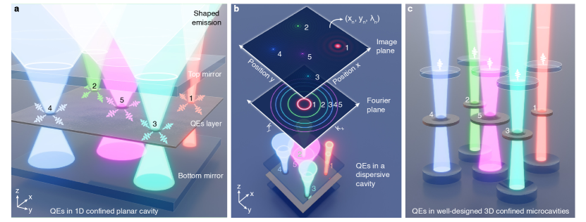
I Principle of snapshot quantum HSI
The concept of snapshot quantum HSI is presented in Fig. 1. Spatial randomly distributed and spectral inhomogeneously broadened solid-state quantum emitters are placed in a 1D nanophotonic planar cavity, as shown in Fig. 1(a). Different from localized micro-cavities in which the lights are highly confined in three dimensions, the nanophotonic planar cavity only provides light confinement in the Z-direction while the photons can freely propagate in the XY plane. The extended mode profile in the XY plane enables couplings between the cavity mode and multiple quantum emitters while the light confinement along the Z direction determines the dispersive feature of the cavity mode. Despite the Purcell factor provided by the planar cavity is very limited due to the rather large mode volume, such a cavity can significantly modify the radiation patterns of the embedded quantum emitters. Due to the dispersive couplings to the cavity modes, the emissions from solid-state quantum emitters (1-5) can only escape from the cavity at specific angles, determined by their emission wavelengths, thus exhibit characteristic far-field radiation patterns in the Fourier plane and unique profiles in the image plane, as presented in Fig. 1(b). Based on the emission characteristics of single quantum emitters modified by the planar cavity mode, it is therefore possible to simultaneously extract the spatial positions () and emission wavelengths () of an ensemble of single quantum emitters by analyzing a snapshot PL image. With the extracted QD parameters, we could consequently realize a much stronger cavity QED effect by removing the original planar cavity and deterministically coupling QDs to 3D confined cavities with significantly reduced mode volumes and pre-designed cavity resonances, as shown in Fig. 1(c).
II Dispersion of a planar DBR cavity
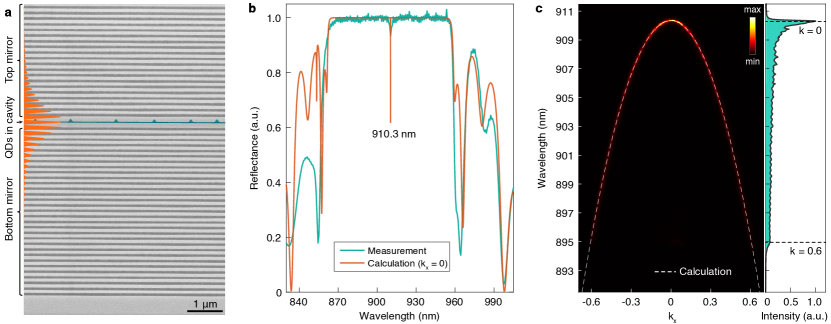
We now implement the concept of snapshot HSI to an III-V semiconductor system in which InAs QDs are embedded in a GaAs/AlGaAs planar cavityramon2006emission ; flagg2009resonantly ; proux2015measuring ; cogan2023deterministic . Such coupled systems have been recognized as superior platforms for fabricating high-performance quantum light sources somaschi2016near ; ding2016demand ; bennett2016cavity ; unsleber2016highly ; he2017deterministic ; liu2021dual ; wei2022tailoring ; gines2022high ; coste2023high and integrated quantum photonic circuitsdusanowski2023chip . As presented in Fig. 2(a), an ensemble of InAs QDs grown by molecule beam epitaxy is embedded in a GaAs layer sandwiched between a bottom and a top distributed Bragg reflector (DBR) consisting of 30 and 20 pairs of 1/4 GaAs/ layer, respectively. The resonant mode of the planar cavity is spectrally located in the middle of the DBR reflection band, as revealed from the reflection spectrum measured along the Z direction in Fig. 2(b). To map the cavity resonance as a function of the in-plane k-vector (radiation direction), we perform angle-resolved spectroscopy zhang2021momentum on an ensemble of QDs under a high excitation power at which the QD ensemble serves as a broadband light source for probing the cavity mode dispersion, see the setups in Fig. E1 of extended data. The radiation direction of the cavity mode is highly correlated to the cavity resonant wavelength and such a dispersion relation can be quantitatively reproduced by the 1D transfer-matrix method (TMM) (see methods), as shown in Fig. 2(c). For comparison, the QDs in bulk material present no dispersion feature in both far-field patterns and image profiles, see Fig. E2 of extended data.
III Snapshot quantum HSI for QDs in a planar DBR cavity
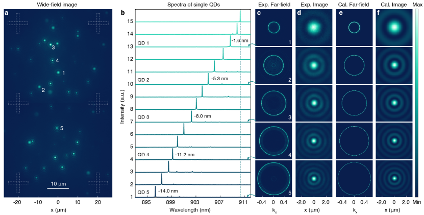
A typical wide-field PL image of the QD ensemble in the planar cavity is collected by a customized microscope and presented in Fig. 3(a). Each individual QD presents itself as a bright spot at a particular position with a specific spot size in the wide-field PL image. The spatial positions of QDs respective to the pre-fabricated alignment marks can be extracted with an accuracy down to 20 nm (see Fig. E3 in the extended data) by using the single molecule super-localization technique which is now widely employed for achieving spatial overlap between the QDs and the optical modes supported by the nanophotonic structures liu2019solid ; liu2021dual ; wei2022tailoring . Here, we focus on the relations between the emission wavelengths, far-field radiation patterns, and image profiles of different QDs. Fig. 3(b) presents confocal PL spectra of 15 individual QDs in the field-of-view, showing sharp exciton emission lines associated with single QDs. The QD spectra are displayed from bottom to top by the order of their emission wavelengths. The measured far-field radiation patterns and image profiles together with the calculations for 5 representative QDs (1-5) with different wavelengths are presented in Fig. 3(c-f), respectively. The single QD emission lines exhibit ring-like far-field patterns due to the couplings to the planar cavity. As the QD emission wavelength moves towards the cavity resonance measured in the Z direction (dashed vertical line), the QD radiation angle (k-vector) decreases and forms an emission ring with a smaller diameter in the far-field, as presented in Fig. 3(c,e). Such a behavior faithfully follows the dispersion characteristics of the planar cavity mode as shown in Fig. 2(c). In contrast, the image profile of single QDs is in the form of an Airy beam consisting of a central bright spot surrounded by concentric rings with decreased intensities in Fig. 3(d,f). Notably, those QDs with short emission wavelengths feature image sizes appreciably smaller than the standard diffraction limit set by the QD emission wavelength and the numerical aperture (NA) of the objetive yang2013minimized (see Fig. E4 in the extended data), which provides a nanophotonic alternative of single-molecule super-resolution microscopy to the well-established technologies based on stimulated emission depletion (STED)vicidomini2018sted ; liu2017amplified ; jin2018nanoparticles ; pu2022super , structured illumination microscopy (SIM)heintzmann2009subdiffraction and single-molecule localization microscopy (SMLM)lelek2021single ; chi2020descriptor ; pertsinidis2010subnanometre . Due to the Fourier-transform relation between the far-field pattern and the image profile, the QD with a larger emission angle exhibits a smaller image size, which consequently correlates the emission wavelength to the image profile.
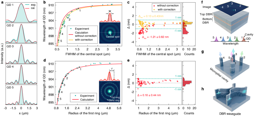
The crosscuts of the PL image profiles in Fig. 3(d, f) are presented in Fig. 4(a) consisting of bright central peaks and weak side lobes. The FWHM of the central peak, w, and the radius of the first ring, r, (the distance between the central peak and the first side lobe) are closely correlated to the QD emission wavelength. We plot the emission wavelength as a function of w and compare the experimental results to the calculations in Fig. 4(b). The red line is the calculation without any free parameter, which matches well with the trend of the experimental data but exhibits a slight offset. By performing a background subtraction in the model (yellow line), we achieve a perfect agreement between the experimental data and the calculation. The necessity of adding a correction in the model is probably due to the weak unwanted emission from other exciton states of QDs which leads to the over-estimation of w. The deviation () of the measured w from the calculated values for QDs with different wavelengths are further presented in Fig. 4(c), in which all the experimental data fall within the 1 nm range of the calculation with a mean value of 0.13 nm and a standard deviation of 0.43 nm when implementing the background subtraction. To avoid any post-correction in the modeling, we investigate the characteristic of the radius of the first ring, r, which is less sensitive to the unwanted background emission in the sample. Without any free parameter and background subtraction, we achieve an excellent agreement between the experiment and the calculation, as shown in Fig. 4(d). The experimental data are well within the 1 nm range of the calculation, showing a deviation () (Fig. 3(e)) with a mean value of 0.1 nm and a standard deviation of 0.44 nm. Based on the relations obtained and verified in Fig. 4(b, d), QD emission wavelengths with an accuracy down to 0.1 nm can be reliably extracted from their image profiles. Therefore, we could simultaneously extract the emission wavelengths and spatial positions of a large number of QDs from a snapshot wide-field PL image. With the employment of snapshot HSI of QDs in a planar cavity (see Fig. 4(f)), we could fabricate a large array of high-performance quantum light sources e.g., single-photon sourcessomaschi2016near ; ding2016demand ; bennett2016cavity ; unsleber2016highly ; he2017deterministic ; liu2021dual ; wei2022tailoring , entangled photon pair sourcesgines2022high and multi-photon entangled sourcescoste2023high , via etching micropillar structures at the QD locations and targeting the cavity resonances to the QD emission wavelengths by controlling the sizes and geometries of the etched micropillars, as schematically shown in Fig. 4(g) and experimentally verified in Fig. E5. In addition, integrated quantum photonic circuits based on DBR waveguides, as shown in Fig. 4(h), can be realized for pursuing on-chip Hong-Ou-Mandel interference between two QDsdusanowski2023chip . Here we emphasize that the spectrometer is only used in Fig. 3(b) to verify our method, it is not needed in the practical implementation of the HIS process.
IV HSI based on opened planar DBR cavity for on-chip quantum circuit
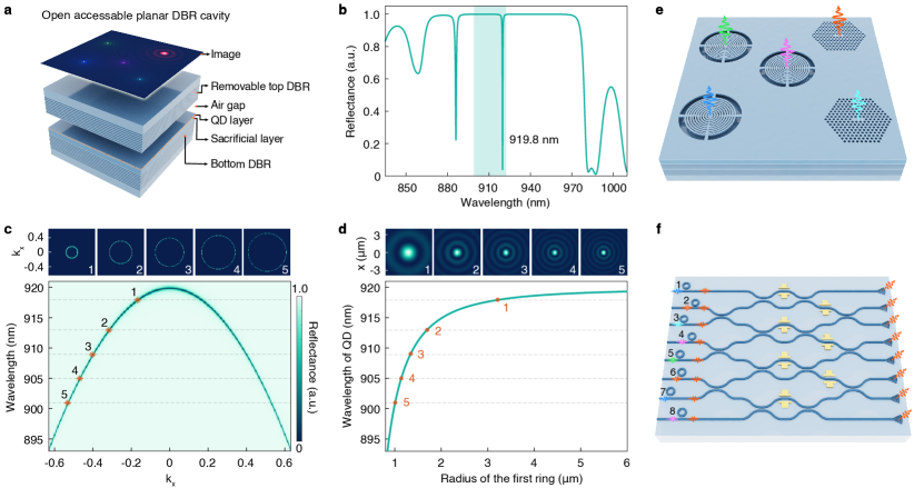
We further show that a proper modification of the cavity configuration could be exploited for building deterministically coupled thin-film QD devices with expanded functionalities and reduced footprints. The proposed planar open cavity is schematically shown in Fig. 5(a). A 180 nm GaAs layer containing InAs QDs and a 450-nm-thick sacrificial layer are grown on a bottom DBR consisting of 20 pairs of 1/4 GaAs/ layer. A movable DBR mirror made of 20 pairs of 1/4 GaAs/ layer is placed on the top of the QD wafer with an air gap of 1000 nm, which could be precisely controlled by a piezo-nanopositionertomm2021bright . The normal reflection spectrum of the proposed planar open cavity is presented in Fig. 5(b), exhibiting two cavity resonances in the stop band. We intentionally designed the fundamental cavity resonance to the proximity of the InAs QD emission wavelength range (895 nm - 920 nm) for HSI. The dispersion diagram of the targeted cavity mode is shown in Fig. 5(c) in which the cavity resonance features a similar dispersion characteristic to that of the planar cavity in Fig. 2(c). By using a microscope objective with an NA of 0.60 (corresponding to a divergence angle of 36.8 degrees), there is a one-to-one correspondence between the emission angle (k-vector) and the emission wavelength. Such a dispersion relation can be further mapped to the relation between the PL image profile and the QD emission wavelength in Fig. 5(d) from which the QD emission wavelength can be directly extracted from the radius of the first ring in the PL image. With the spatial and spectral information of QDs obtained from the HSI, suspended membrane cavities with deterministically coupled QDs, such as circular Bragg resonators and high-Q photonic crystal cavities, can be fabricated for state-of-the-art quantum light sources and strong light-matter interactions (see Fig. E6 of extended data), as schematically shown in Fig. 5(e). To avoid the suspended membrane structures for large-scale integrations, more scalable devices such as microring quantum frequency convertors, phase shifters, interferometers and grating couplers, as shown in Fig. 5(f), can also be pursued by transferring the thin GaAs layer containing QDs on a low-index insulator substratecastro2022expanding (see Fig. E7 of extended data).
V Conclusion
To conclude, we’ve extended the HSI concept from classical optics to advanced quantum technologies by simultaneously extracting both spatial and spectral information of multiple solid-state quantum emitters from a snapshot wide-field PL image. We experimentally perform HIS of QDs in a planar cavity towards the realization of an extensive array of deterministically coupled QD-micropillar quantum light sources and integrated quantum photonic circuits based on DBR waveguides. To build integrated quantum photonic circuits with reduced footprints and expanded functionalities, such as frequency converters, phase shifters, interferometers and grating couplers, we propose and numerically demonstrate the feasibility of snapshot HSI of QDs in a planar open cavity. Our HSI technique can be straightforwardly adapted to other types of solid-state quantum emittersaharonovich2016solid , e.g., NV centers, single molecules, and defects in GaN or 2D materials for high-throughput optical characterizations sutula2023large . More generally, it is also possible to implement snapshot HSI into biophysics where fast tracking and identification of single fluorescent particles are highly desirable yet technologically challenging. Our work provides an unprecedented tool to advance both classic optics and quantum photonics by enabling high-throughput deterministic light-matter interactions at the nanoscale.
VI methods
Modeling: To calculate the far-field and image profile of the emission escaped from the planar DBR cavity, the parameters of the cavity are first extracted by fitting the measured reflectivity spectrum with a transform matrix method (TMM) mackay2022transfer , as shown in Fig. 2(b). The cavity dispersion along the x-direction is then modeled by calculating the angle dependence reflectivity/transmission spectrum of the cavity (Fig. 5(c)), which gives the relation between the QD emission wavelength and its momentum space distribution. For a specific wavelength, the calculated 1D far-field distribution is straightforwardly extended to a 2D far-field profile (XY plane) by performing rotation transformation, considering the structure symmetry, as presented in Fig. 3(e). The corresponding image profile is obtained by performing a Fourier transformation to the far-field profile within the angle defined by the NA of the objective. The FWHM of the central spot and the radius of the first airy ring are then extracted from the calculated image profile.
Optical characterizations: The schematic of the setups for optical characterizations is presented in Extended Data Fig. E1.
Data availability
The data that support the findings of this study are available within the paper and the Extended Data. Other relevant data are available from the corresponding authors on reasonable request.
Acknowledgements
This research was supported by National Key Research and Development Program of China (2021YFA1400800); National Natural Science Foundation of China (62035017, 12304409), the Guangdong Special Support Program (2019JC05X397), and the National Super-Computer Center in Guangzhou.
Author Contributions
J. L. conceived the project; S. F. L., J. L., and H. Q. L. designed the epitaxial structure and the devices; H. Q. L. and H. Q. N. grew the quantum dot wafers; S. F. L. and G. X. Q. developed the theory model and calculated the image and far-field profile; S. F. L. and X. S. L. fabricated the devices; S. F. L. built the setup and performed the optical measurements with inputs from X. S. L., J. T. M., and L. N.; S. F. L. and J. L. analyzed the data; J. L. and S. F. L. prepared the manuscript with inputs from all authors; J. L., Z. C. N., C.-W. Q. and X. H. W. supervised the project.
Conflict of Interest
The authors declare no conflict of interest.
References
- (1) Schulte, C. H. et al. Quadrature squeezed photons from a two-level system. Nature 525, 222–225 (2015).
- (2) Tiranov, A. et al. Collective super-and subradiant dynamics between distant optical quantum emitters. Science 379, 389–393 (2023).
- (3) Tomm, N. et al. Photon bound state dynamics from a single artificial atom. Nat. Phys. 19, 857–862 (2023).
- (4) O’brien, J. L., Furusawa, A. & Vučković, J. Photonic quantum technologies. Nat. Photon. 3, 687–695 (2009).
- (5) Wang, J., Sciarrino, F., Laing, A. & Thompson, M. G. Integrated photonic quantum technologies. Nat. Photon. 14, 273–284 (2020).
- (6) Uppu, R., Midolo, L., Zhou, X., Carolan, J. & Lodahl, P. Quantum-dot-based deterministic photon–emitter interfaces for scalable photonic quantum technology. Nat. Nanotechnol. 16, 1308–1317 (2021).
- (7) Zhou, X., Zhai, L. & Liu, J. Epitaxial quantum dots: a semiconductor launchpad for photonic quantum technologies. Photon. Insights 1, R07–R07 (2023).
- (8) Englund, D. et al. Controlling cavity reflectivity with a single quantum dot. Nature 450, 857–861 (2007).
- (9) Lodahl, P., Mahmoodian, S. & Stobbe, S. Interfacing single photons and single quantum dots with photonic nanostructures. Rev. Mod. Phys. 87, 347 (2015).
- (10) Javadi, A. et al. Single-photon non-linear optics with a quantum dot in a waveguide. Nat. Commun. 6, 8655 (2015).
- (11) Sun, S., Kim, H., Luo, Z., Solomon, G. S. & Waks, E. A single-photon switch and transistor enabled by a solid-state quantum memory. Science 361, 57–60 (2018).
- (12) Li, C. et al. Arbitrarily structured quantum emission with a multifunctional metalens. eLight 3, 19 (2023).
- (13) Somaschi, N. et al. Near-optimal single-photon sources in the solid state. Nat. Photon. 10, 340–345 (2016).
- (14) He, Y.-M. et al. Deterministic implementation of a bright, on-demand single-photon source with near-unity indistinguishability via quantum dot imaging. Optica 4, 802–808 (2017).
- (15) Wang, H. et al. Towards optimal single-photon sources from polarized microcavities. Nat. Photon. 13, 770–775 (2019).
- (16) Liu, J. et al. A solid-state source of strongly entangled photon pairs with high brightness and indistinguishability. Nat. Nanotechnol. 14, 586–593 (2019).
- (17) Wang, H. et al. On-demand semiconductor source of entangled photons which simultaneously has high fidelity, efficiency, and indistinguishability. Phys. Rev. Lett. 122, 113602 (2019).
- (18) Uppu, R. et al. Scalable integrated single-photon source. Sci. Adv. 6, eabc8268 (2020).
- (19) Tomm, N. et al. A bright and fast source of coherent single photons. Nat. Nanotechnol. 16, 399–403 (2021).
- (20) Vajner, D. A., Rickert, L., Gao, T., Kaymazlar, K. & Heindel, T. Quantum communication using semiconductor quantum dots. Adv. Quant. Technol. 5, 2100116 (2022).
- (21) Wang, H. et al. Boson sampling with 20 input photons and a 60-mode interferometer in a -dimensional hilbert space. Phys. Rev. Lett. 123, 250503 (2019).
- (22) Müller, M. et al. Quantum-dot single-photon sources for entanglement enhanced interferometry. Phys. Rev. Lett. 118, 257402 (2017).
- (23) Wang, H. et al. Observation of intensity squeezing in resonance fluorescence from a solid-state device. Phys. Rev. Lett. 125, 153601 (2020).
- (24) Gao, W., Fallahi, P., Togan, E., Miguel-Sánchez, J. & Imamoglu, A. Observation of entanglement between a quantum dot spin and a single photon. Nature 491, 426–430 (2012).
- (25) De Greve, K. et al. Quantum-dot spin–photon entanglement via frequency downconversion to telecom wavelength. Nature 491, 421–425 (2012).
- (26) Azuma, K. et al. Quantum repeaters: From quantum networks to the quantum internet. arXiv preprint arXiv:2212.10820 (2022).
- (27) Afzelius, M., Gisin, N. & De Riedmatten, H. Quantum memory for photons. Phys. Today 68, 42–47 (2015).
- (28) Coste, N. et al. High-rate entanglement between a semiconductor spin and indistinguishable photons. Nat. Photon. 17, 582–587 (2023).
- (29) Cogan, D., Su, Z.-E., Kenneth, O. & Gershoni, D. Deterministic generation of indistinguishable photons in a cluster state. Nat. Photon. 17, 324–329 (2023).
- (30) Liu, S., Srinivasan, K. & Liu, J. Nanoscale positioning approaches for integrating single solid-state quantum emitters with photonic nanostructures. Laser Photonics Rev. 15, 2100223 (2021).
- (31) Gerard, J.-M. & Gayral, B. Strong purcell effect for InAs quantum boxes in three-dimensional solid-state microcavities. J. Lightwave Technol. 17, 2089 (1999).
- (32) Englund, D. et al. Controlling the spontaneous emission rate of single quantum dots in a two-dimensional photonic crystal. Phys. Rev. Lett. 95, 013904 (2005).
- (33) Badolato, A. et al. Deterministic coupling of single quantum dots to single nanocavity modes. Science 308, 1158–1161 (2005).
- (34) Hennessy, K. et al. Quantum nature of a strongly coupled single quantum dot–cavity system. Nature 445, 896–899 (2007).
- (35) Kuruma, K. et al. Position dependent optical coupling between single quantum dots and photonic crystal nanocavities. Appl. Phys. Lett. 109, 071110 (2016).
- (36) Thon, S. M. et al. Strong coupling through optical positioning of a quantum dot in a photonic crystal cavity. Appl. Phys. Lett. 94, 111115 (2009).
- (37) Dousse, A. et al. Controlled light-matter coupling for a single quantum dot embedded in a pillar microcavity using far-field optical lithography. Phys. Rev. Lett. 101, 267404 (2008).
- (38) Kolatschek, S. et al. Deterministic fabrication of circular bragg gratings coupled to single quantum emitters via the combination of in-situ optical lithography and electron-beam lithography. J. Appl. Phys. 125, 045701 (2019).
- (39) Gschrey, M. et al. Highly indistinguishable photons from deterministic quantum-dot microlenses utilizing three-dimensional in situ electron-beam lithography. Nat. Commun. 6, 7662 (2015).
- (40) Kojima, T., Kojima, K., Asano, T. & Noda, S. Accurate alignment of a photonic crystal nanocavity with an embedded quantum dot based on optical microscopic photoluminescence imaging. Appl. Phys. Lett. 102, 011110 (2013).
- (41) Sapienza, L., Davanço, M., Badolato, A. & Srinivasan, K. Nanoscale optical positioning of single quantum dots for bright and pure single-photon emission. Nat. Commun. 6, 7833 (2015).
- (42) Liu, J. et al. Cryogenic photoluminescence imaging system for nanoscale positioning of single quantum emitters. Rev. Sci. Instrum. 88, 023116 (2017).
- (43) Pregnolato, T. et al. Deterministic positioning of nanophotonic waveguides around single self-assembled quantum dots. APL Photonics 5, 086101 (2020).
- (44) Yildiz, A. et al. Myosin V walks hand-over-hand: single fluorophore imaging with 1.5-nm localization. science 300, 2061–2065 (2003).
- (45) Ramon, G. et al. Emission characteristics of quantum dots in planar microcavities. Phys. Rev. B 73, 205330 (2006).
- (46) Flagg, E. B. et al. Resonantly driven coherent oscillations in a solid-state quantum emitter. Nat. Phys. 5, 203–207 (2009).
- (47) Proux, R. et al. Measuring the photon coalescence time window in the continuous-wave regime for resonantly driven semiconductor quantum dots. Phys. Rev. Lett. 114, 067401 (2015).
- (48) Ding, X. et al. On-demand single photons with high extraction efficiency and near-unity indistinguishability from a resonantly driven quantum dot in a micropillar. Phys. Rev. Lett. 116, 020401 (2016).
- (49) Bennett, A. J. et al. Cavity-enhanced coherent light scattering from a quantum dot. Sci. Adv. 2, e1501256 (2016).
- (50) Unsleber, S. et al. Highly indistinguishable on-demand resonance fluorescence photons from a deterministic quantum dot micropillar device with 74% extraction efficiency. Opt. Express 24, 8539–8546 (2016).
- (51) Liu, S. et al. Dual-resonance enhanced quantum light-matter interactions in deterministically coupled quantum-dot-micropillars. Light Sci. Appl. 10, 158 (2021).
- (52) Wei, Y. et al. Tailoring solid-state single-photon sources with stimulated emissions. Nat. Nanotechnol. 17, 470–476 (2022).
- (53) Ginés, L. et al. High extraction efficiency source of photon pairs based on a quantum dot embedded in a broadband micropillar cavity. Phys. Rev. Lett. 129, 033601 (2022).
- (54) Dusanowski, Ł., Köck, D., Schneider, C. & Höfling, S. On-chip hong–ou–mandel interference from separate quantum dot emitters in an integrated circuit. ACS Photon. 10, 2941–2947 (2023).
- (55) Zhang, Y. et al. Momentum-space imaging spectroscopy for the study of nanophotonic materials. Sci. Bull. 66, 824–838 (2021).
- (56) Yang, L., Xie, X., Wang, S. & Zhou, J. Minimized spot of annular radially polarized focusing beam. Opt. Lett. 38, 1331–1333 (2013).
- (57) Vicidomini, G., Bianchini, P. & Diaspro, A. STED super-resolved microscopy. Nat. Methods 15, 173–182 (2018).
- (58) Liu, Y. et al. Amplified stimulated emission in upconversion nanoparticles for super-resolution nanoscopy. Nature 543, 229–233 (2017).
- (59) Jin, D. et al. Nanoparticles for super-resolution microscopy and single-molecule tracking. Nat. Methods 15, 415–423 (2018).
- (60) Pu, R. et al. Super-resolution microscopy enabled by high-efficiency surface-migration emission depletion. Nat. Commun. 13, 6636 (2022).
- (61) Heintzmann, R. & Gustafsson, M. G. Subdiffraction resolution in continuous samples. Nat. Photon. 3, 362–364 (2009).
- (62) Lelek, M. et al. Single-molecule localization microscopy. Nat. Rev. Methods Prim. 1, 39 (2021).
- (63) Chi, W. et al. Descriptor GC-O enables the quantitative design of spontaneously blinking rhodamines for live-cell super-resolution imaging. Angew. Chem. 132, 20390–20398 (2020).
- (64) Pertsinidis, A., Zhang, Y. & Chu, S. Subnanometre single-molecule localization, registration and distance measurements. Nature 466, 647–651 (2010).
- (65) Castro, J. E. et al. Expanding the quantum photonic toolbox in AlGaAsOI. APL Photonics 7, 096103 (2022).
- (66) Aharonovich, I., Englund, D. & Toth, M. Solid-state single-photon emitters. Nat. Photon. 10, 631–641 (2016).
- (67) Sutula, M. et al. Large-scale optical characterization of solid-state quantum emitters. Nat. Mater. (2023). URL https://doi.org/10.1038/s41563-023-01644-8.
- (68) Mackay, T. G. & Lakhtakia, A. The transfer-matrix method in electromagnetics and optics (Springer Nature, 2022).