The design and performance of the ZEUS Micro Vertex Detector
Abstract
In order to extend the tracking acceptance, to improve the primary and secondary vertex reconstruction and thus enhancing the tagging capabilities for short lived particles, the ZEUS experiment at the HERA Collider at DESY installed a silicon strip vertex detector. The barrel part of the detector is a 63 cm long cylinder with silicon sensors arranged around an elliptical beampipe. The forward part consists of four circular shaped disks. In total just over 200k channels are read out using of silicon. In this report a detailed overview of the design and construction of the detector is given and the performance of the completed system is reviewed.
keywords:
ZEUS, Silicon, Microstrip, Tracking, VertexingPACS:
29.40.Gx, 29.40.Wk, 07.05.Fb, 07.05.Hd, , , , , , , , , , , , , , , , , , , , , , , , , , , , , , , , , , , , , , , , , , , , , ,
, , , , , , , , , , , , , , , , , , , ,
1 Introduction
In the HERA storage ring GeV positrons or electrons collide with protons. The ZEUS experiment [2, 3] is one of two large multi-purpose collider detectors installed at HERA. From 1992 to 2000 HERA delivered ca. of luminosity and the ZEUS experiment recorded ca. 180 million collision events. Following the successful completion of that program in 2000 the accelerator and the experiments underwent an extensive upgrade during 9 months in 2000/2001 with the goal to achieve a five-fold increase in integrated luminosity by 2006.
As part of the upgrade of the ZEUS experiment, the tracking capabilities were enhanced by the installation of a Microvertex Detector (MVD) inside the existing Central Tracking Detector (CTD). The goal was to provide the experiment with the capability of tagging heavy quarks by identifying displaced vertices. In addition the aim was to improve the efficiency, acceptance and resolution of the tracking system. During the design phase the following requirements were specified in order to achieve that goal:
-
•
Polar angular coverage between ;
-
•
Three spatial measurements per track, in two projections;
-
•
intrinsic hit position resolution for normal incident tracks;
-
•
Impact parameter resolution of about for tracks with polar angle of , increasing gradually to mm at , for tracks with momenta greater than ;
-
•
Noise occupancy ;
-
•
Hit efficiency ;
-
•
Alignment accuracy better than ;
-
•
Two-track separation better than .
A number of constraints also had to be taken into account. These were
-
•
The space available for the Microvertex Detector is limited by the inner bore of the central tracking detector (diameter );
-
•
The longitudinal size of the HERA beam spot extends over about ;
-
•
The readout electronics and therefore also cooling and cabling have to be located very close to the sensors to cope with the bunch crossing time of HERA;
-
•
The detector and the frontend electronics need to operate inside a 1.4 T axial magnetic field.
The geometrical layout of the MVD consists of a barrel (BMVD) and a forward (FMVD) section. Here we note that the ZEUS coordinate system is right-handed with the -axis along the incoming proton beam direction, the -axis in the horizontal plane pointing to the inside of the HERA ring and the -axis pointing upwards. The barrel section, centered at the interaction point, is about cm long. The silicon sensors are arranged in three concentric cylindric layers. The innermost layer is incomplete in the polar angle range of around the positive -axis. The forward section is composed of four vertical planes extending the angular coverage down to 7∘ from the beam line. Access for cables and cooling is arranged from the rear.
The ZEUS MVD was built in a collaboration of several institutes within the context of the ZEUS collaboration during 1997 through 2000. It was installed inside ZEUS in the spring of 2001. In the fall of 2001 the detector recorded first events. From then until the end of HERA operation in June 2007 the detector has been successfully operated over a period of almost 6 years. During that time a luminosity of approximately was collected and more than 600 million electron-proton scattering events were recorded using the detector.
In the following sections we give a comprehensive description of the different detector subsystems and we discuss how the requirements set forth were met taking the constraints into account. We also adress the conclusions that we have drawn. The following detector subsystems will be described in detail:
-
•
Silicon Sensors,
-
•
Readout Electronics,
-
•
Mechanical Construction,
-
•
Data Acquisition System,
-
•
Slow Control,
-
•
Radiation Protection,
-
•
Data Quality Monitoring,
-
•
Alignment and Tracking.
At the end we show some representative physics results obtained with the detector and we end with a conclusion.
2 Silicon Sensor Design
The design of the silicon sensors of the ZEUS MVD as well as the prototype and acceptance tests have been described in detail in [4]. Here we just summarize the main features of the sensors and give some additional information on the ideas behind the design chosen.
Three different sensor geometries have been designed: square sensors for the barrel part (BMVD), and two wedge shaped sensors for the forward part (FMVD) of the detector. Table 1 gives the relevant geometrical parameters.
| type | shape | dimensions | strip length | # of readout strips | active area |
|---|---|---|---|---|---|
| BMVD |
![[Uncaptioned image]](https://cdn.awesomepapers.org/papers/72e10e0e-1778-4b85-82aa-7e3a88908d7f/bmvd_geom.png)
|
h=64.2mm w=64.2mm | 62.2mm | 512 | 38.6cm2 |
| FMVD1 |
![[Uncaptioned image]](https://cdn.awesomepapers.org/papers/72e10e0e-1778-4b85-82aa-7e3a88908d7f/fmvd1_geom.png)
|
h=73.5mm w1=64.3mm w2=30.7mm | 5.6 - 73.3mm | 480 | 32.6cm2 |
| FMVD2 |
![[Uncaptioned image]](https://cdn.awesomepapers.org/papers/72e10e0e-1778-4b85-82aa-7e3a88908d7f/fmvd2_geom.png)
|
h=48.5mm w1=64.1mm w2=42.0mm | 5.6 - 47.4mm | 480 | 23.9 cm2 |
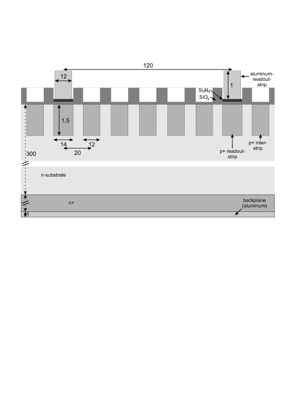
Apart from their geometry, the three sensor types are identical. They are single-sided strip detectors on high ohmic n-type silicon. The readout pitch is with 5 intermediate strips for capacitive charge division. The p+-readout strips are AC-coupled through a SiO2-Si3N4 double layer to Al-strips, which are connected via wire bonds either to a Polyimide foil with Cu strips (Upilex [5]) or a glass fan-out. The p+-readout strips and the p+-intermediate strips are connected individually via poly-silicon resistors to the biasing ring. Three p+-guard rings surround the biasing ring. The innermost guard ring is connected resistively to ground and collects the current from defects outside of the sensor’s sensitive volume. The two outer guard rings are left floating. Outside of the last guard ring an n+-line is placed which allows biasing the detector from the top. The most important parameters of the sensors are given in Table 2; a sketch of the cross section is shown in Figure 1. The sensor design was guided by the following ideas:
Analog readout was chosen because of available experience in the group and the greater ease with which noise, pickup and general performance could be understood. After exploring different options the HELIX 128-v3 chip [6] was selected for the frontend readout;
Single-sided readout was chosen because of the ease of mechanical mounting, the larger number of vendors of sensors, costs and, last but not least, because of a tight time schedule. The compromise of an additional % of a radiation length per two dimensional coordinate, which increases secondary interactions and multiple scattering, was considered an acceptable compromise;
The readout pitch of and need of serial bonding of two sensors for the BMVD was dictated by the maximum number of readout channels due to space, the amount of inactive material in the path of the particles and the cooling requirements. Capacitive charge division with 5 intermediate strips [7] with pitch does not present a technological challenge for sensor production on the one hand, on the other hand it results in a nearly linear charge sharing between the readout strips. Thus the position resolution is fairly independent of the particle’s passage relative to the readout strip and is essentially determined by the combined sensor and readout noise. A disadvantage of the capacitive charge division is, that the measured total pulse height varies by about as a function of the particle passage relative to the readout strips. Another feature of the readout scheme chosen is that the position resolution depends only weakly on angle up to about 30∘. Simulations have shown, that for single detectors at normal incidence a position resolution of is expected for the BMVD-type detectors. The simulation also shows that the position resolution is directly proportional to the readout noise. Thus a significant worsening is expected if two detectors are put in series via a Upilex cable as done for the BMVD;
The performance of single BMVD detectors has been studied in detail in an electron test beam of maximum energy at the DESY electron synchrotron [8, 9, 10]. For hits with pulse heights below 1.7 times the most probable value (to avoid degradation due to delta electrons) a resolution of has been measured for normal incidence. After correcting for multiple scattering and the resolution of the beam telescope, an intrinsic resolution of has been obtained. In addition the spatial resolutions and pulse height distributions for incident angles from to have been investigated. The results show that the resolution is below for angles up to . If a “head-tail algorithm” [8, 11] is used, a resolution below for angles up to is achieved. The results are compatible with simulations which take into account the fluctuations of the charge deposition along the particle track, the readout noise and the electric network of the detector and the readout amplifiers [11, 9];
Similar test beam measurements [11] have been performed with BMVD half modules (see section 4), in which two BMVD sensors are connected in series by a Upilex cable. As expected from the simulations the increase in readout noise due to the increased capacitance worsens the spatial resolution to about at normal incidence;
A particular feature of the sensor design is that both bonding and probe pads are inside the sensitive sensor volume. As the width of these pads is 75 m they couple capacitively to the intermediate strips in a different way than the strips themselves. Using SPICE simulations, in which the detector is simulated by a three-dimensional RC network coupled to the small signal model of the HELIX chip, it has been shown that during the shaping time the charge spreads approximately along the strips, resulting in a change of the position resolution for tracks passing the bond pads [11, 12];
Finally the choice of interconnecting sensors with orthogonal strips (see Section 4) was chosen as it meant a significant simplification of the sub-module construction. Monte Carlo simulations showed, that such a design neither increases the number of ambiguous tracks nor causes significant complications for the track reconstruction.
The sensors have been produced by Hamamatsu Photonics K. K. [13]. For details of the measurement of the technological parameters and the acceptance tests we refer to [12, 4]. We just mention here, that for the acceptance tests the depletion voltage, the maximum detector currents and their stability in a long term test have been measured for every detector. In parallel to production, test structures were measured to verify technology parameters and the radiation sensitivity.
Throughout the production the quality of the detectors has been excellent.
| sensor type | n-type Si, single sided p+ implants |
| resistivity | kcm |
| depletion voltage | V |
| depth active volume | d = m |
| readout strips | Al on p+ strips, AC coupled ( double layer) |
| p+ readout strip pitch | m |
| p+ readout strip width | m |
| number of interstrips | 5 |
| p+ interstrip width | m |
| Al readout strip width | m |
| backplane | deep n+ layer, aluminized |
| strip biasing | poly-Si resistor |
| number of guard rings | 3 |
3 Readout Electronics
In addition to the reasons given in the previous section analog readout also has the added benefit of measuring the specific energy loss of different particle species in the detector’s sensitive volume. In the following the different components of the readout electronics, namely the hybrids with the frontend chips, the patchboxes, the analog link, the ADC and the clock and control systems are described in more detail.
3.1 Helix Chips and Hybrids
The HELIX 128-v3 chip has been selected for the frontend readout. The HELIX was originally developed by the ASIC Labor Heidelberg for the HERA-B experiment. It was designed in CMOS technology and was manufactured by AMS [14]. In the following only the general features of the HELIX chip are described. More details can be found in [6, 15].
One HELIX chip contains 128 channels, each having its own charge-sensitive preamplifier, a shaper and a 141-cell analog pipeline. The bias settings and various other parameters which determine the shaping time, signal and gain can be adjusted using programmable DACs. The chip runs at clock speed synchronized to the HERA bunch crossing cycle. Roughly speaking, it works in the following manner: Once receiving a trigger, the corresponding 128 analog data signals in pipeline cells are sent out over a single analog line synchronized with the clock. At the end of the transfer, an 8-bit trailer encoding the cell location is generated. Several chips can be daisy-chained. In that mode, signals from several chips are multiplexed and read out over one analog line. In case of ZEUS, 8 chips are chained together.
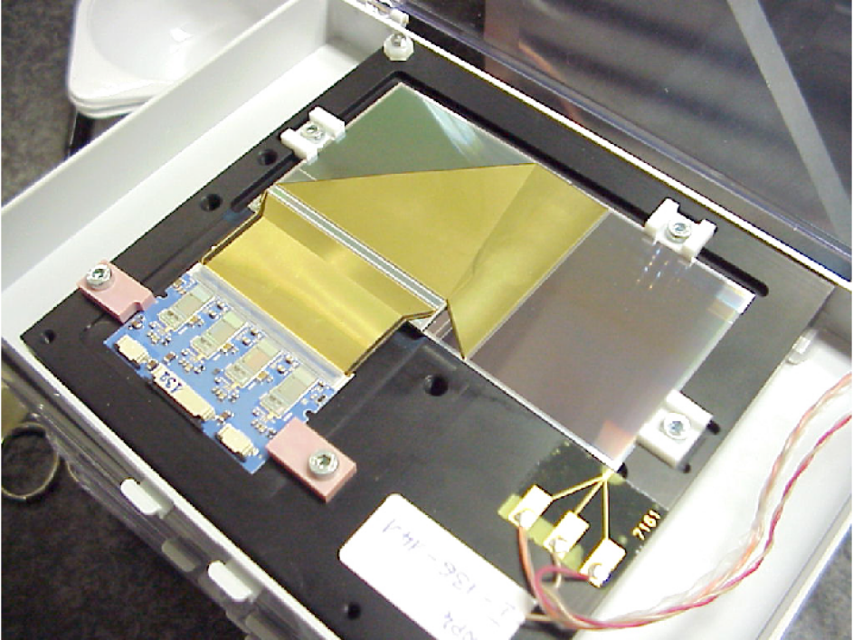
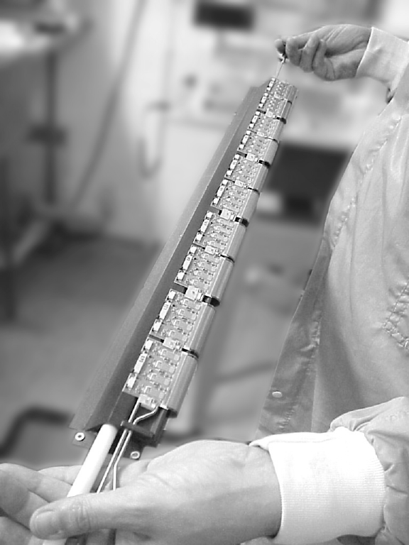
Four chips are hosted on a ceramic hybrid board which provides bias and supply voltages and routes control and output signals. The sensors are connected to the hybrids through a flexible Upilex cable and a glass pitch adaptor. A photograph of a barrel half module attached to a pair of sensors is shown in Figure 2.
3.2 Cabling, Patchboxes and Shielding
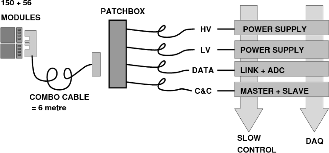
Figure 3 shows a sketch of the readout chain of the detector downstream of the detector modules. Supplies and signals as well as sensor lines for temperature and humidity are routed along the rear part of the ZEUS beampipe over a distance of ca. using customized “COMBO” cables made by Axon [16]. In the barrel the connection between the ceramic hybrids and the COMBO cables is done using a pitch flex PCB and miniature ZIF connectors. This solution was chosen due to the severe space constraints. In the forward section of the detector these constraints are less severe and hence standard PCBs were chosen. Just outside the ZEUS detector on the rear side the COMBO cables are connected to four patch boxes where bias and supply voltages as well as data and control cables are split up. The COMBO cables provide double shielding and in addition groups of COMBO cables are routed inside conductive zipper tubes for additional protection against electromagnetic interference. Also, the cables running from the patchboxes to the readout racks some away are doubly shielded. This careful shielding allowed to keep the entire analog signal chain from the sensors to the backend readout system outside the detector without active elements. This approach was deemed necessary since the frontend of the detector is not easily accessible and it was planned to operate it for a period of five years without intervention. In retrospect this approach has proven very successful.
3.3 Analog Link
The total number of analog signal lines in the detector amounts to 206. Each HELIX chip also provides an analog dummy output which follows almost identical circuitry but is not connected to the sensors and lacks the first preamplification stage. Both outputs of the HELIX daisy-chain are subtracted and amplified by an analog link board which feeds it to the ADC module. This analog subtraction takes care of the dominant contribution of the common noise. After the subtraction the signal range is , which corresponds to .1111 MIP corresponds to about 24,000 electrons at the amplifier input.
3.4 ADC Module Design
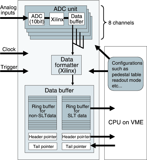
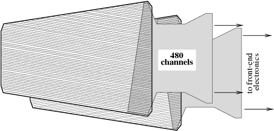
The ADC module design is described in detail in [17]. Only a brief description is given here. A schematic view of the ADC module is shown in Figure 4. One ADC module processes 8 analog input channels. Each ADC unit (ADCU) handles one analog input line. It consists of a 10-bit analog-to-digital converter (AD9200) and a data processor implemented in a programmable gate array (the XC4028EX of XILINX). The processed data are stored in FIFOs. A data formatter, implemented in another XC4028EX, reads out the FIFOs of all ADCUs and writes formatted data into data buffers, which are accessible from the VME bus.
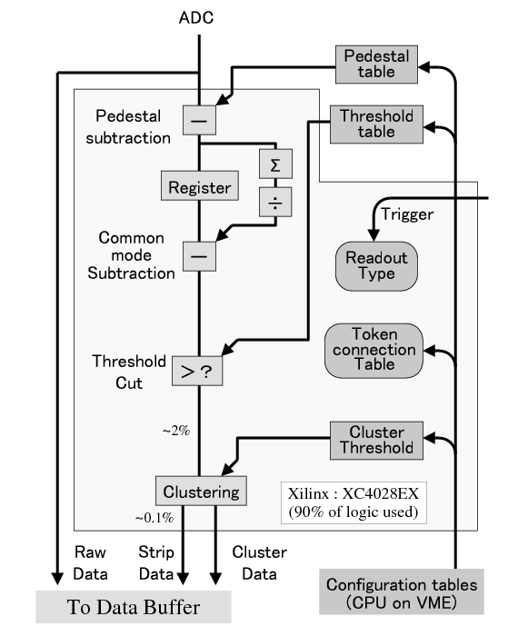
The data processor in the ADCU is similar to that described in [18]. The block diagram of the data processor is shown in Figure 5. First, 10-bit ADC data are processed for pedestal and common mode subtraction. (At this level, after the analog subtraction in the Analog Link, the common noise is typically very small.) Then, strips with charge greater than a seed threshold are kept for cluster finding. A second cluster threshold is set for the total charge of the cluster before further data reduction. The size of the input raw data volume is reduced to about 2% after the threshold cut and to about 0.1% after the cluster cut. An ADCU has 3 FIFOs for the output data: for raw data, for strip data which consist of strip ID and ADC values after the processing, and for cluster data which contain the total charge and the location of the cluster.
The performance of the analog part is monitored with the internal charge injection of the HELIX which generates a repetitive pattern equivalent to +2MIP, +1MIP, -1MIP and -2MIP in each channel. The digital processing part is tested separately with digital test patterns stored in memory implemented in the module.
3.5 Clock and Control
The clock and control system (C&C) consists of three parts: These are the master and the slave timing controllers, the helix driver modules and the active electronics inside the patch boxes. Figure 6 shows a schematic of the system. In the following the major components of the system are briefly described. Many more details may be found in [19].
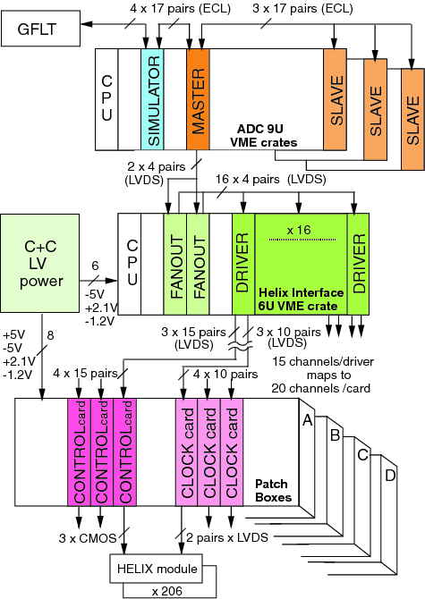
The master and slave timing modules handle the fanout of the trigger and clock signals from the ZEUS Global First Level Trigger (GFLT). The main functions of the C&C master are to receive the standard GFLT information and to pass it on to the C&C slaves, decode the trigger information in order to produce and send the relevant signals to the HELIX fanout modules together with a correctly timed ns clock and to handle the ERROR and BUSY signals from the ADCs. Additionally, the C&C master is able to operate in a stand-alone mode for test purposes, generating its own ns clock. The C&C slaves receive the GFLT signals from the C&C master and distribute them to all the ADCs within their crates and they receive back the BUSY and the ERROR lines from the ADCs. They also distribute the suitably timed ns clock synchronously to all the ADCs in their crates, via a specially wired-in set of 16 twisted pairs of identical length, to front panel connectors. The C&C slaves also allow a continuous VME read access to a register with the ADC-produced signals. Additionally, the C&C slaves can operate with the C&C master as a standalone system for test purposes.
16 Helix Driver Modules are located in a separate VME crate. Each Helix Driver module generates the required controls signals for 15 Helix channels from the clock and control commands received from the C&C master via two Helix Fanout modules. Programming information for the Helix modules in the detector is sent along the VME back-plane to the Helix Drivers, then after some processing to the Patchboxes and on to the detector. The five C&C signals are CLOCK, TRIGGER (this doubles as the Serial Data line during downloading), TEST PULSE, LOAD and .
Each Helix Driver board carries two Programmable Logic Devices (PLDs), one of which contains the VME interface electronics, and the other, the on-board processing logic, status registers, etc. The incoming signals are treated as follows: The clock signal is fanned to 15 clocks, one for each channel, and each with its own programmable delay unit. The purpose of these is to remove timing skews at the detector. The trigger signal is counted, then OR-ed with the serial data line used for downloading. The combined signal is then sent to all 15 channels. The test pulse is expanded to 15 channels, which are compared with a mask register, then the unmasked ones output to selected channels. The is OR-ed with an internally generated signal used during downloading. The combined signal is sent to all channels.
The C&C boards in the patchboxes both have active components. The five signals per channel arriving from the Helix Drivers are slightly degraded at the end of the 20 meter cables, and in the case of the clock boards, the signals are re-generated by a receiver-transmitter combination (LVDS to CMOS/LVDS) before being sent down the micro-cable twisted pairs to the Helix Modules. This precaution is necessary due to the relatively high attenuation factor of the micro-cables.
4 Mechanical Construction
4.1 Overall layout
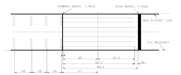
The mechanical layout of the MVD consists of a barrel and a forward section. A sketch of the cross section along the beam line is shown in Figure 7.We recollect that the ZEUS coordinate system is right-handed with the -axis along the incoming proton beam direction, the -axis in the horizontal plane pointing to the inside of the HERA ring and the -axis pointing upwards.
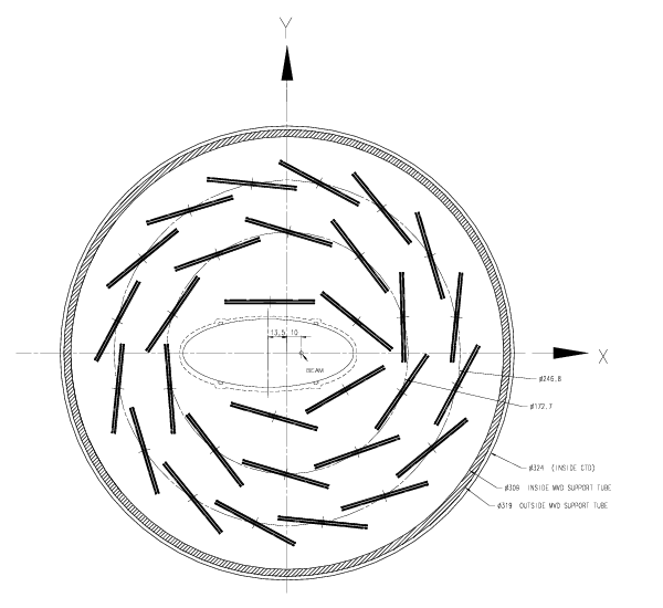
The barrel section, centered at the interaction point, is about cm long. The silicon sensors are arranged in three concentric cylindric layers. As shown in Figure 8, approximately 25% of the azimutal angle is covered by only two layers due to limited space. The polar angular coverage for tracks with three hits ranges from 300 to 1500. The modules in the forward section are arranged in four vertical planes extending the angular coverage down to 7∘ from the beam line. Exits for cables and cooling is arranged from the rear. Many details, design drawings and pictures can be found in [20].
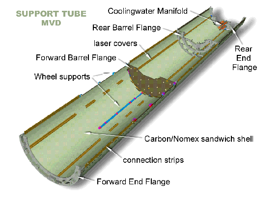
4.1.1 Support tube
The MVD had to fit inside the inner cylinder of the Central Tracking Detector (CTD), a cylinder with a diameter of 324 mm. The only available support points are located at the forward and the rear side of the CTD, a span of . To make efficient use of the available space it was decided to install the MVD and the beampipe together; the support for the MVD has then to be made in two halves. The two half cylinders are joined together, providing a stiff support for the whole assembly. During and after installation the weight of the beampipe has to be taken by external supports.
The support tube is an assembly of light weight half cylinders connected to each other via flanges. A thick honeycomb layer is glued between two carbonfiber ( thick) sheets and preformed on a cylindrical mold in an autoclave. During this process the inside and outside of the tube is covered with a thick aluminium layer for electric shielding. Figure 9 shows a sketch of one half of the support tube.
4.2 Barrel modules
Details on the silicon sensors, their characteristics and performance are described in Section 2.
Two sensors are glued together and one sensor is electrically connected to the other as shown in Figure 10, forming a half module. For various reasons we chose to orient the readout strips of the two sensors within one half module perpendicular to each other as shown in Figure 10. A Cirlex [21] strip (, thick) glued at the edge in between the sensors, forms the mechanical connection between the two. The use of this material ensures a good insulation of the HV side of one sensor from the ground plane of the other one.
While the sensors overlap by , the sensitive areas only overlap by . Cirlex feet, with a cross section of a few square mm and varying in thickness from 0.8 to , are used to connect the sensors to the support structure.
The electrical connection between the two sensors is made via copper traces on a thick Upilex foil. The foil is precisely aligned, glued on the sensors and subsequently wire bonded to the strips. The connection of the sensor assembly with the frontend readout is also made via a Upilex foil, glued at one side on a sensor and at the other side on the hybrid as indicated in Figure 10.
A surface of forms one readout cell of 512 channels and is called a half module. A mirror image of this half module is also shown in Figure 10; both are mounted on top of each other, separated by the spacers mentioned above forming a full module with 1024 readout channels.
Two precision markers, glued to each half module, provide reference points for the alignment on the support structure.
4.2.1 Barrel module assembly
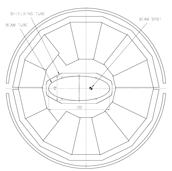
The area covered by the silicon in the barrel section is long and is formed by two cylinders with radii of approximately 125 and . The coverage is realized with segments of arranged like roof tiles, such that there are no gaps in azimuth angle between adjacent segments for the outer two cylinders. A third layer close to the beampipe provides a coverage of about in azimuth angle. Figure 8 shows a cross section of the silicon sensors in the barrel section.
Five full modules are fixed side by side, with gaps in between, on a support frame and form a “ladder”. The modules are glued to the ladder with the spacers mentioned earlier.
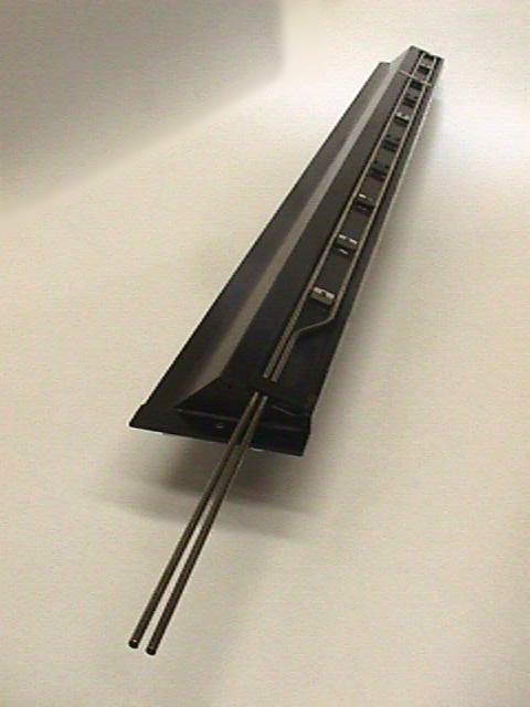
The frontend electronics, cabling and cooling are attached to the support frame that holds the modules: a ladder. In order to conserve the high resolution properties of the silicon sensors a support structure that bends less than when all components are mounted was required.
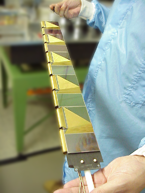
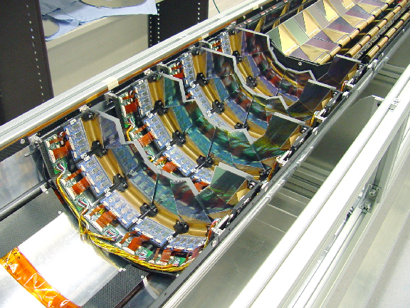
The total weight to be carried by one ladder, silicon plus electronics, cooling and cabling is . The cross section of the support structure is triangular to accommodate a support for the hybrids and cooling, providing at the same time the necessary stiffness. Carbonfiber material (five layers of fiber with a total thickness of ) is used to realize a strong and lightweight construction. Strips of carbonfiber material with variable width and approximately length are cut from the sheets and glued together with the help of a mold to form a ladder. No deformation has been observed as a function of humidity or temperature changes. Figure 11 shows the bare ladder with water cooling pipe (details about the water cooling are described in section 6), a stainless steel tube with 0.1mm wall thickness. Figure 12 shows the ladder with the sensors mounted, while Figure 13 shows the mounting of the frontend electronics; the flexible Upilex connection between sensor and hybrid allows fixation of the hybrid on the side of the ladder on top of the cooling pipes. Table 3 gives an overview of the parts forming the barrel detector.
| inner cylinder | medium cylinder | outer cylinder | Totals | |
| radius(mm) | 90 | 125 | ||
| number of ladders | 4 | 10 | 16 | 30 |
| number of silicon sensors | 80 | 200 | 320 | 600 |
| number of readout cells | 40 | 100 | 160 | 300 |
| number of readout channels | 20480 | 51200 | 81920 | 153600 |
| number of readout chips | 160 | 400 | 640 | 1200 |
| (128 channels/chip) |
4.3 Forward modules
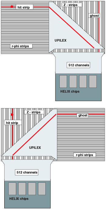
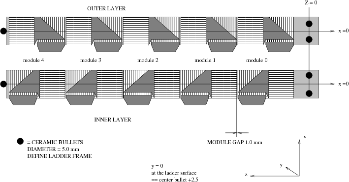
Apart from their shape the silicon sensors covering the forward region are similar to the barrel sensors as described in Section 2. Fourteen wedge-shaped sensors cover a circular plane around the beampipe. Figure 14 shows the geometry of one sensor, together with the Upilex foil guiding the signals to the hybrid. The strips run parallel to one tilted side; each sensor has a total of 480 readout strips with readout pitch. Figure 15 shows the geometric layout of the sensors for one wheel.
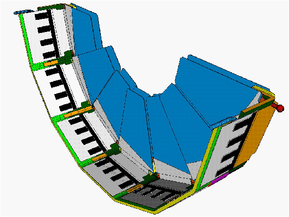
The FMVD consists of four planes perpendicular to the beam axis; each plane has two sensor layers. Adjacent sensors are displaced perpendicular to the beam line by and overlap in azimuth by ( in sensitive area). The two layers are mounted back to back on a support structure, separated by approximately in Z-direction. Figure 16 shows a sketch of the layout of one half of a wheel. The sensors are mounted on an L-shaped carbon fiber half ring, with seven straight sections. Aluminum inserts in the short ’leg’ of the ring guarantee precision holes for the positioning of the sensors. These are put back to back, such that the angle between the strips is . The long side of the L-shaped support provides housing for the cooling pipes and supports the hybrids. The half wheels are supported at three points inside the main support tube.
Tab. 4 summarizes the main parameters of the wheel geometry and the statistics of the individual parts.
| outer radius(mm) | 132mm |
| inner radius(mm) | 60mm |
| wedge angle | 13∘ |
| readout strip pitch | 120 m |
| number of channels/sensor | 480 |
| number of sensors/wheel | 2 x 14 |
| number of wheels | 4 |
| total number of sensors | 112 |
| total number of readout channels | 53760 |
| number of readout chips | 448 |
| (128 channels/chip) |
Figure 17 shows four half wheels mounted in the support structure.
4.4 Material distribution
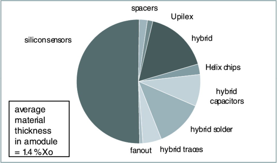
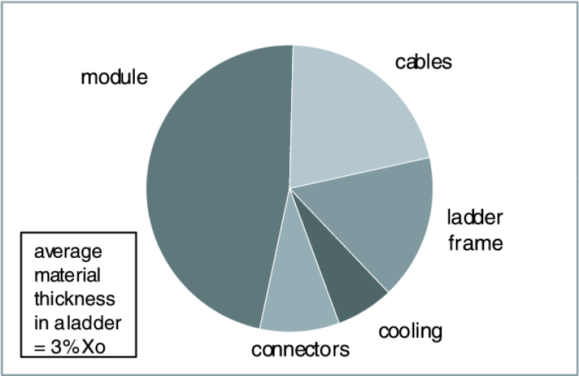
The material distribution has been calculated for individual modules and complete ladders and is summarized in Figs. 18 and 19. If all the material which makes up a module is equally distributed over its surface, the total thickness represents of a radiation length; for a ladder this amounts to (including the modules).
5 Data Acquisition
The architecture of the MVD data acquisition system [22] has been strongly influenced by its contribution to the ZEUS trigger. The ZEUS data acquisition system is based on a three level trigger. Because of the HERA bunch crossing rate of , i.e. between consecutive bunch collisions, the experiment uses a pipelined readout design. The Global First Level Trigger (GFLT), based on a reduced set of information from the detector components, is issued synchronously after 46 bunch crossings and reduces the trigger rate to . Detector data, stored in deadtime-free analog or digital pipelines, is subsequently digitized, buffered and used by the Global Second Level Trigger (GSLT). The GSLT lowers the trigger rate to with a typical latency of . For accepted events the complete detector information is read out, merged with data from other detector components by the Event Builder (EVB) and sent to the Third Level Trigger (TLT) computer farm where event reconstruction and final online selection are performed. In normal conditions the total deadtime caused by the detector and trigger components is about . More details on the ZEUS trigger and data acquisition system can be found in [23].
5.1 The Global Tracking Trigger
Simulation studies on data multiplicity and background had shown that the MVD data alone, providing up to 3 planes of information per track, would not be sufficient for unambiguous tracking and efficient rate reduction. Combining the MVD information with the surrounding tracking detectors would instead allow a far better rate reduction and tracking efficiency. These considerations have lead to the design within the MVD data acquisition system of the Global Track Trigger (GTT) [24], a distributed computing environment processing data from the MVD, the Central Tracking Detector (CTD) and the newly installed forward Straw Tube Tracker (STT).
For the computing infrastructure, the preferred choice has been to use whenever possible, commercial off the shelf equipment easily upgradable and maintainable. Investigations on the performance achievable in terms of data throughput, process latency and performance suggested a solution based on embedded VME computers running a realtime operating system for the data readout and a farm of standard PCs connected via a Fast/Gigabit Ethernet network for trigger and data processing.
For the readout platform Motorola PowerPC single board CPUs and the LynxOS operating system were chosen due to the following requirements:
-
•
Realtime Unix-like operating system;
-
•
Network boot and diskless operation;
-
•
Reliable Fast Ethernet network operation;
-
•
Fast and flexible DMA and Interrupt capable VMEbus bridge.
28 MVD ADC modules are organized in three 9U VME crates for BMVD upper, BMVD lower and FMVD respectively. These crates receive clock and trigger information via the Clock and Control Slave Module located in the same crate. This system is described in more detail in Section 3.5. A short overview is repeated here. Busy and error conditions are set by the ADC modules and the VME processor and sent through the Slave Module to the Master Module. The Master module is directly connected to the GFLT, and transmits clock and trigger information both to the readout and to the MVD front end and can be operated via VME to allow standalone MVD running. Data gathering from the CTD and STT systems, both of which are based on a network of transputers222INMOS Transputers, were an advanced technological development in the late 80’s when the ZEUS experiment was designed. Provided with a 32 bit processing unit, on board memory, four 20 MHz serial links for processor interconnection and a high level parallel programming language (OCCAM), transputers were ideal for highly distributed parallel processing and data transfer. hosted in several VMEbus crates, is done using the same VMEbus computers [25].
On GFLT accept, event data from MVD, CTD and STT are sent to one GTT processor where the required trigger calculations are performed. The GTT result is forwarded to another PowerPC VME computer which re-orders the events according to the GFLT number and transfers the result to the GSLT. Since the GSLT is also based on a transputer network a similar solution as for the CTD and the STT was adopted. No special hardware is required to receive the GSLT trigger decision as this is transferred back via TCP/IP. An interface process forwards it to the MVD readout CPUs and the GTT processors. On GSLT accept the full MVD and GTT data are sent to the EVB interface. It merges and formats these data into the final format. Performance and data quality monitoring is also performed on this system. The specific hardware components of the MVD DAQ and the GTT systems are summarized in Table 5.
| Number | Item | Purpose |
|---|---|---|
| Detector readout and data gathering: | ||
| 3 | Motorola MVME2400 450MHz 64MB | MVD Readout (9U ADC VMEbus crates) |
| 3 | Motorola MVME2400 450MHz 64MB | CTD axial, CTD z by timing, STT data |
| GTT processing: | ||
| 10 | SuperServer 6014P Dual 3GHz 1GB | GTT Algorithm Processing |
| 1 | DELL PowerEdge 4400 Dual 1GHz 256MB | GTT Server+Credit/GSLT Decision |
| 1 | Motorola MVME2400 450MHz 64MB | GTT to GSLT Trigger Result Interface |
| 1 | DELL PowerEdge 4400 Dual 1GHz 256MB | Data collection and EVB interface |
| Supporting network and processing infrastructure: | ||
| 1 | DELL PowerEdge 6450 Quad 700MHz 1GB | NFS File Server, Process Hub and Run Control |
| 1 | DELL PowerEdge 4400 Dual 1GHz 256MB | EVB interface and online monitoring |
| 1 | Motorola MVME2700 367MHz 64MB | LynxOS Boot Server and Development Node |
| 1 | Motorola MVME2700 367MHz 64MB | HELIX frontend programming and monitoring |
| 2 | Intel Express 480T Fast/Giga-16Port Cu Switch | Network Connections |
| 2 | CISCO XXX switches | Network Connections |
5.2 The VMEbus Readout Software
In order to fully exploit the VMEbus access capabilities of the on-board Tundra universe II VME bridge, a dedicated software package for VMEbus access on Motorola PPC boards running LynxOS was developed [26]. The package consists of a library layered on an enhanced driver with respect to the default version distributed by LynxOS, providing flexible VME memory mapping, DMA transfer and queueing, VME interrupt and process synchronization control in a multi-user environment. User programs perform all VME and related operations using the library without any direct connection to the driver.
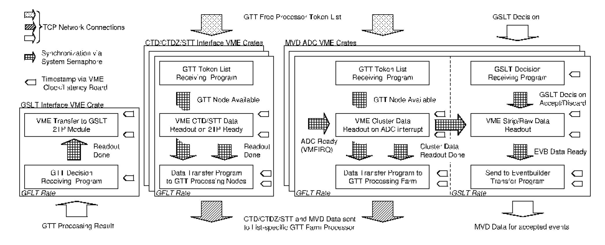
Within the library, basic data structures to describe Shared Memory Segments opened both on the internal contiguous memory and on the VMEbus are available for standard and DMA-controlled read-write cycles. An additional interface is provided to support process synchronization by waiting on, or setting system semaphores. It is possible to connect VME interrupt handling to system semaphores, identically treating synchronization to hardware interrupts, DMA cycles or software signals. The ability to uniquely identify segments by ID or name allows many processes to connect to already existing mapped regions (up to eight in the VME space) without overloading the system. These features have allowed a modular design in a complex DAQ environment. A diagram of the main processes running on the VME computers when taking data is shown in Figure 20.
On the ADC systems two software pipelines running at FLT and SLT rates respectively, exist. At FLT rate the readout program running at lower priority, is woken up on VME interrupt as soon as data are ready on the ADC boards. After data has been transferred via DMA to internal memory, the network tasks, synchronized by a semaphore and running at a higher priority, will send the data to the GTT farm. A similar software pipeline is available also on the CTD and STT interfaces for the data read out at GFLT rate.
5.3 The GTT Environment Process
The GTT, as any of the components participating in the ZEUS second level trigger, has to process events at an average rate with a mean latency, including all the data transfers, of less than and small tails due to busy events or performance fluctuations.
The GTT environment process is a multi-threaded program with one thread per input data source (MVD, CTD, STT), one thread per trigger algorithm and a time limit thread. Typically one environment runs on each of the dual CPU farm PCs. The scheduling of dispatching data to environments is organized using a synchronized ordered list rather than a round-robin scheme. The decision for that mechanism was based on simulation studies.
For development and performance tests a playback capability has been provided: This allows one to feed simulation or previously saved events into the component VME interfaces and into the GTT trigger chain.
All network data transfers are performed using standard TCP/IP protocol. To cope with the different platforms involved (PowerPC for the VME readout and standard PC for the DAQ and GTT computing nodes) the communication and synchronization is done via short XDR encoded messages while detector data is sent with no additional overhead. To monitor the readout latencies and network transfer times precisely, a general purpose 6U VME board [27] providing a latency/clock register, has been developed and installed in all VME crates and connected to a common clock bus. Thus absolute timestamps and latency measurements are available for every event and stored in the data at several points of the data acquisition phase. This allows a detailed monitoring of the system performance. During normal running a mean latency smaller than with steep tail for the whole GTT system, compatible with the initial requirements is observed.
5.4 Computing Environment and Software
As described previously the DAQ computing environment consists of VME board computers running LynxOS and Intel PCs running Linux interconnected via point-to-point Fast or Gigabit Ethernet. The VME systems are diskless and are booted over the network from a single, dedicated, VME system acting as a boot server. All Linux systems are booted from local disks. In order to simplify code usage a single DAQ file system, containing executable directories etc., is mounted via NFS by all participating hosts.
Standard C programming has been used throughout the DAQ and GTT systems. A number of ROOT-based C++ GUIs have been developed to control the DAQ system in stand-alone mode, to view online or archived histograms, and to manually control the detector slow control system, etc.
All non-readout or trigger data messages are transmitted through a hub process and not directly between processes. The hub is a multi-threaded process which accepts connections at a known address and enforces a simple protocol, using XDR.
5.5 Run and Process Control
The MVD run control can run in either standalone mode or as part of the ZEUS run control system. In both cases process control, stopping and starting tasks, is facilitated by daemon processes started at boot time. These advertise themselves to the run control system and identify, by name, processes they are capable of running. Run configuration requests from ZEUS or the standalone run control specify a Runtype definition file naming all the processes to be started or stopped, the parameters they require, their required exit status, etc. The C preprocessor (cpp) is then invoked to expand all of the definitions contained in the file (resolving required processes, their supporting daemon, startup parameters, etc.). The file produced corresponds to a sequential list of process control commands required to perform all the transitions specified. The run control system can then sequence all the steps required for each transition request received. Transition requests fail if a process fails to reach or does not remain in its final state.
6 Slow Control
Power supplies and other devices required for operating the MVD are controlled and monitored by the slow control system. The field bus used to communicate with devices is CANbus, which implements a serial data transfer protocol with differential signal levels. All devices used are located at the MVD rack platform and the maximum bus length is 10 m. Three ESD CAN-PCI/331 [28] dual CANbus adapters located in two Linux PCs provide the seven buses used to individually connect all devices. By connecting devices from the same manufacturer to a bus, baudrate and CANbus addressing incompatibilities were avoided. The slow control devices are described below followed by a brief description of the software used.
6.1 Silicon detector bias voltage
A commercial high voltage system [29] is used to provide bias voltage to the silicon detectors. Four 6U EURO crates (ISEG ECH 238L UPS), with eight voltage boards (ISEG EHQ F0025p) of 16 outputs each provide the 412 channels that are required to supply each silicon half module independently. The output voltage range is 0 to V, adjustable in steps of mV. The maximum current is mA. The nominal detector bias voltage and trip settings were V and , respectively. The measurement resolutions of nA and mV allow accurate detector I-V curves to be generated for use in monitoring radiation damage. Two CANbus buses are used; one to connect the four crate controllers, and another to connect the voltage boards via the crate backplanes.
An additional non-crate mounted voltage board supplies the MVD radiation monitor diodes. This device is connected separately to CANbus.
The ability to control the properties of single and groups of output channels simultaneously was used extensively during commissioning of the detector. During data taking this flexibility was not required.
6.2 Helix hybrid low voltage
The frontend hybrid low voltage system is a custom development derived from the system used by the ZEUS Leading Proton Spectrometer detector [30]. Six 6U EURO crates, each with 8 voltage boards of 10 outputs provide the 206 channels required to supply V to each hybrid board with a maximum current of A. CANbus is interfaced to the internal bus at the crate controller board.
An additional crate, whose boards are modified to output V and V, is used to supply voltage to the Helix clock and control interface electronics. The CANbus of this crate is connected to the bus used by the hybrid low voltage system. More details can be found in [31].
As with the bias system, single channel control was useful during commissioning the detector.
6.3 Hybrid cooling
The system used to cool the detector readout hybrids is a custom implementation using closed freon and water circuits. It is designed to remove energy dissipated by the helix hybrids in the barrel (300 W) and wheels (120 W). The cooling system is controlled and read out through a programmable logic device (PLD), whose serial peripheral interface (SPI) bus is interfaced via a NIKHEF SPICAN [32] module to CANbus. The PLD continuously monitors environmental (pressure, temperature, humidity, airflow, etc.) parameters associated with the cooling system, and switches off the cooling if an error threshold is exceeded. Cold water, 11.5 ∘C, is piped to the detector and distributed via a manifold to ladder and wheel cooling pipes; warm water is returned to the cooling system input. The entire system is flushed continuously with dry air in order to avoid condensation. A detailed description of the system including pictures can be found in [33].
6.4 Beampipe and hybrid temperature
NTC sensors are used to monitor 18 beampipe and 72 hybrid mounted sensors. The system’s SPI bus is interfaced via a NIKHEF SPICAN module to CANbus. The temperature readout system shares the cooling system’s CANbus. During data taking the barrel and wheel hybrid temperatures are typically 18 and 27 ∘C, respectively.
6.5 Safety interlocks
The safety interlocks used are designed to ensure that the MVD low and bias voltages are off during injection or if a hardware failure occurs. In the off state no power from the MVD slow control system is dissipated in the detector. A Frenzel+Berg Easy-30 SPS/CAN [34], connected by a separate CANbus, switches off the power to the hybrid low and bias voltage crates if one of the 4 bi-metal relays (60∘) mounted on the MVD support opens or if the cooling is off.
Slow control signals are additionally connected to the experiment’s interlock control which prevents beam injection if the MVD is on. Additional signals disable the trigger if the slow control is not in the configured state. Note that the experiment’s interlock system has no CANbus interface and the open/close (alarm/no alarm) signals are driven by logic connected to CST-DI8-TTL and CST-DO8-TTL input/output drivers [35] connected to a separate CANbus. If the 5 second duty cycle clock driven from the CST control software stops then injection and triggers are disabled.
6.6 Software
The slow control system reuses the hub based software developed for the run control system. Each sub-system control task has associated with it a hub public name, which allows new configuration messages to be sent and monitoring information to be received.
Configuration messages can be sent from scripts, a ROOT GUI, and via the Slow Control Control (SCC) system. SCC acts as a scheduler for slow control operations performed on more than one sub-system. During operation the cooling system remains on and the detector is switched between ON (voltages set) and STANDBY (zero volts) states by SCC. Additionally, the SCC drives the interlock levels such that when the detector is not in STANDBY injection is disabled, and when the detector is neither ON nor in STANDBY the trigger is disabled.
Monitoring information is made available via html query requests for tabulated statistics derived from messages held in the hub, or from histograms showing long term evolution of parameter values. This information and additional logfile data are archived.
7 Radiation Protection
Due to the sensitivity towards radiation damage of MVD components, its close position to the beams and the much increased risks of radiation damage compared to HERA I running a new radiation monitoring system was developed [36]. The main sources of radiation are the synchrotron radiation passing through the detector causing possible damage by direct or back-scattered radiation, off-momentum leptons and proton beam-gas interactions. In addition partial or total uncontrolled beam losses are sources of severe damages. The purpose of the radiation monitoring system is to
-
•
monitor the background conditions continously with an experiment-independent data aquisition;
-
•
instantly generate a dump request signal for the lepton machine as soon as background conditions are too bad.
The proton machine operates its own protection system which protects the experiments as well. The rare uncontrolled losses cannot be intercepted by dump requests.
7.1 Radiation sensitive components
The two most radiation sensitive components of the MVD are the Si sensors and the CMOS-based readout chips mounted inside the MVD volume. The sensitivity of the sensors has been tested using hadronic (reactor neutron irradiations) and ionising radiation ( 60Co photon irradiation) [37].
After the neutron irradiation with up to cm-2 (much higher than the hadronic background expected during the MVD lifetime) no type inversion showed up as expected. After 3 weeks of annealing the leakage current had reached a value . After the 60Co irradiation the leakage current reached 425 A which reduced to A after 25 days of annealing. Testbeam measurements showed no change in performance of the sensors in terms of resolution and reduction of S/N [10].
As discussed earlier, the readout is based on the custom designed CMOS chip HELIX128-3.2 [15] designed in the AMS CYE 0.8 micron [14] process. One has therefore to expect changes of threshold voltages and transconductances of the MOS transistors for irradiations in the 1 kGy range. The design does not use any radiation tolerant layout techniques. On the other hand the setting of the transistors of the most sensitive parts of the design can be controlled by programmable DACs which can compensate the effects of irradiations to some extent.
For the irradiation of the Helix chips a test module was used consisting of only one sensor with the hybrid connected which carries the Helix chips The hybrid was tested in a separate 60Co photon irradiation up to 5 kGy [38]. Figure 21 shows the S/N-ratio and the intrinsic position resolution as a function of the accumulated dose. The setting determining the bias current of the preamplifier is labelled and the setting determining the feedback resistance of the shaper is labelled .
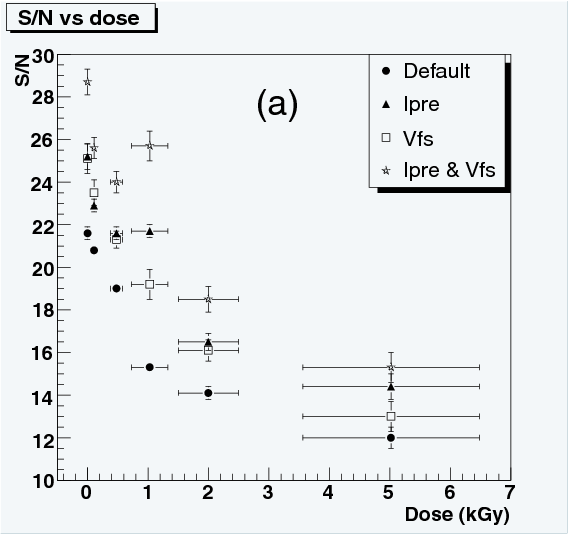
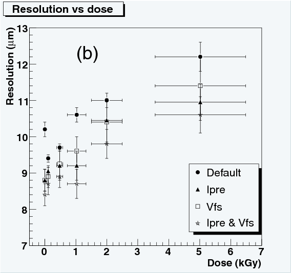
A deterioration of the performance after irradiation was observed, and the single track resolution for perpendicular incidence in a single diode worsens from before irradiation to after 5 kGy. By optimising the programmable readout parameters, the resolution after irradiation can be improved to . The resulting performance was thus still within the specified range [38].
In summary both sensitive parts of the MVD can survive a dose of more than 1 kGy before the performance deteriorates considerably. Since the MVD was foreseen to operate for five years at ZEUS a dose of more than 20 Gy/s could be safely allowed assuming a year of seconds duty time.
7.2 Dose rate measurement
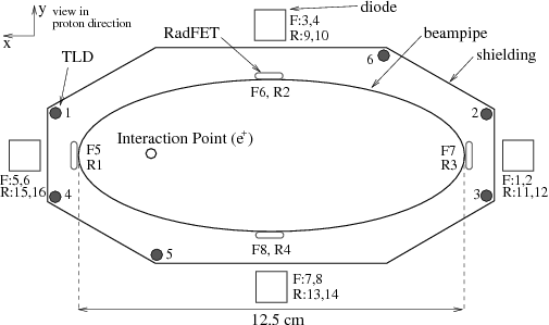
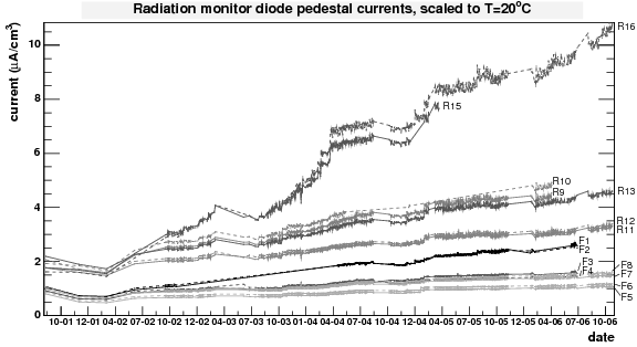
The radiation monitor consists of 16 Si pin diodes of size [39] arranged in 8 pairs and mounted inside the MVD volume as shown in Figure 22. The two diodes of each pair are separated by of Pb to provide a discrimination between currents produced by mips and photons. Each pair of diodes is equipped with an NTC resistor to provide a temperature measurement for leakage current corrections. The diodes are connected via a m doubly shielded cable to the data aquisition and HV supplies. Initially the diodes have been reverse-biased at V. Later the voltage was reduced to V (February 2005) to allow for more stable running conditions.
The current measured in the reverse-biased diodes consists of the rate of energy deposited in the diodes and of the leakage currents. Assuming an energy of eV for the production of one electron-hole pair the dose rate and the current are related by
| (1) |
The deposition of energy in the diodes leads to radiation damage which results in an increase of the leakage current. At the time of writing the original leakage currents of below 1 nA have increased to about nA at V biasing for diodes on the inside of the ring.
The currents are fed into a two stage integrating amplifier whose voltages are measured by a commercial ADC with a resolution of mV/nA. The range of the ADC reaches up to V allowing a maximum current of nA corresponding to mGy/s dose rate. The leakage currents are monitored regularly with no beams in the storage ring. The measured leakage currents, corrected for temperature, are the basis of the dose measurements. For the monitoring and the control of the dump signals the so called leaky-bucket concept developed by the BaBar experiment [40] is used. This concept allows a certain amount of excursions of the dose rate. The dump signal is released only after a certain deposited dose. Above a threshold of Gy/s, the integration of the dose rate starts. A dump signal will be issued only if a dose of mGy has been reached. To control the dose for rates below the threshold human intervention is needed.
Initially a software driven system with a s sampling rate was used. In 2006 a new DAQ system was installed which reduces the reaction times from seconds to milliseconds thereby reducing the received doses before dumping.
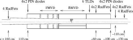
7.3 Dose measurement
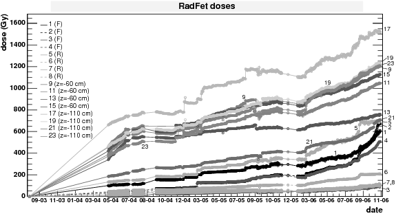
In parallel to the current measurement two integrating systems have been installed at the beginning of the operation of the MVD: thermoluminescent dosimeters(TLD) and radiation field effect transistors (RadFet) [41]. The positions are indicated in Figure 22. Whereas the TLDs have to be exchanged regularly for reading, the RadFets can be read out continously by a remote data aquisition. Two types of TLDs have been used:
-
•
7LiF (TLD-700) being sensitive to ionising radiation
-
•
and 6LiF (TLD-600) being sensitive to both ionising radiation and thermal neutrons by means of capture.
In the shutdown in March 2003, 20 months after the beginning of the HERA II operation, all RadFets were exchanged. In addition another type of RadFet was installed at and which can be read out continously [41]. The TLDs were not used after March 2003.
7.4 Measurements and Results
All dose rate and dose related measurements show a very non-uniform distribution. The highest values are found at the ring inside at negative , supporting simulations which predict a high rate of off-momentum leptons (Figure 23). The trigger rates of the ZEUS experiment show the same dependency. The total dose received at cm for the ring inside position is approximately kGy. The doses measured with the TLDs until 2003 are in general agreement with the RadFet measurements. The diodes at cm and cm which were installed later, received kGy and kGy respectively. During the same period the diodes at cm received kGy. Between the two positions and cm a scintillator-lead sandwich at cm and vacuum flanges act as an extra collimator and can therefore explain the different dose values.
The performance of the MVD modules shows a similar tendency as the dose measurements: a small increase of noise for modules in cylinder 0 at the ring inside positions and negative -position (Figure 26) decreasing from negative to positive position leading to a decrease of S/N of up to %. A total dose of close to kGy as measured by the RadFets would have led to a decrease of the S/N of about %. The difference can be understood by the fact that the Radfets are positioned as close as mm to the beam whereas the readout electronics of cylinder 0/ladder 0 has a distance of close to mm from the beam.
8 Data Quality Monitoring
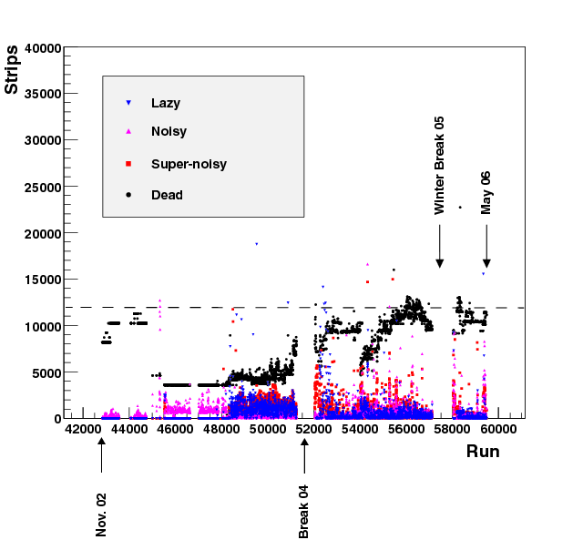
A three level data quality monitoring system has been developed for the ZEUS MVD in order to ensure an optimal level of data integrity under all running conditions. At the first level a fraction of the data are inspected and relatively simple quantities like occupancy histograms, hit maps and signal distributions are quickly calculated. These quantities are constantly monitored by the ZEUS shift crew. The second level monitoring is tied to the archiving step of the data: All data that pass the Third Level Trigger are inspected just after they have been written to the ZEUS offline archive. At this stage every strip in the detector is inspected and classified. Any strip whose behaviour in terms of noise or average occupancy deviates from the expected normal behaviour is classified according to one of four categories.
These are:
- Lazy:
-
The occupancy of the strip is significantly below the expectation as calculated from an average over a set of neighbouring strips.
- Noisy:
-
The noise is outside 2.8 standard deviations of the expectation.
- Super-noisy:
-
The noise is outside 3.5 standard deviations of the expectation
- Dead:
-
There are no hits.
Using this classification, channels marked as “super-noisy” are excluded during the track reconstruction in order to simplify the pattern recognition step.
Fig. 24 shows the number of differently flagged channels as a function of run number over a period of almost four years. It can be seen that after an initial rise the number of flagged channels now fluctuates up and down below a level of ca. 12000 with no obvious tendency. This level corresponds to approximately of all channels of the detector. The origin of these malfunctions is in the frontend of the detector, the hybrids and cables. These are not accessible from the outside without a major disassembly of the ZEUS detector. These malfunctions are not completely understood. However, the observed failure pattern, namely the fact that typically entire half modules fail, indicates that the problem is inside the flex PCB connecting the hybrids to the COMBO cables. This failure mode occurs almost exclusively in the barrel region (8 failed modules and 6 failed half-modules in the barrel compared to only 2 failed wheel sectors) It is suspected that the presence of hygroscopic glue which was used in the barrel but not in the wheels may have destroyed some of the vias.
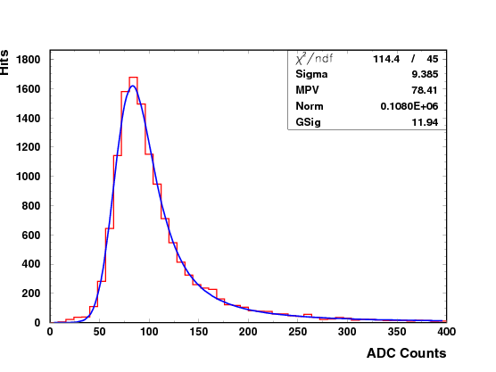
The third level of DQM occurs after track reconstruction inside the reconstruction program. Tracks are used to filter hits which are associated with charged particles originating from the interaction vertex. This hit sample is very clean. In addition the association of hits with tracks allows one to normalize the signals to track length inside the silicon. Fig. 25 shows signals for these hits corrected for track length. This distribution is well described by a Landau function with a most probable value around 78 ADC counts convoluted with a Gaussian. The latter takes care of the simultaneous presence of signal and noise for the hits.
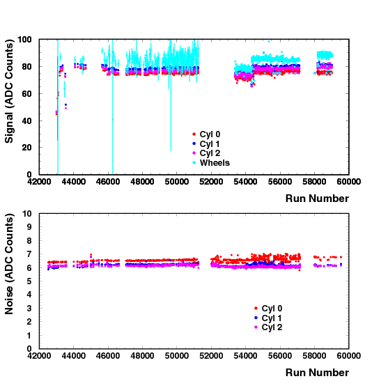
Figs. 26(a) and (b) show the behaviour of signal and noise over time, respectively. With the exception of a few jumps in the signal level, both signal and noise are stable with time. The jumps occur following a calibration of the sampling delay in the ADC system relative to the maximum position of the signal pulse.
9 Alignment and Tracking
9.1 Tracking
The offline track reconstruction beyond the local coordinate level consists of the track pattern recognition, the track fit, the vertex finding and the vertex fit. The track pattern recognition makes full use of the track finding powers of the individual detectors and proceeds through a complex multipass algorithm which combines CTD, forward and barrel MVD in a transparent way. This has the advantage that the track finding efficiency of the CTD is effectively enhanced by the MVD. Seeds are constructed from superlayers of both systems, and the resulting initial trajectories are then used to collect additional hits. In the MVD, also seeds consisting partly of barrel and partly of forward MVD hits are constructed to cover the transition area. Track candidates with ample hit information from both CTD and MVD take precedence, but also tracks composed entirely from MVD or CTD hits are found in later passes of the procedure, which extends the range beyond the CTD acceptance. The information assigned to a track then enters the track fit [42], which is based on the Kalman filter method. The track fit determines the accurate track parameters and their covariances taking the detailed material distribution of the MVD and the beampipe elements into account. Effects from both multiple scattering and ionization energy loss are accounted for. The track fit also rejects outlier hits based on their contribution to the fit. Also the vertex finder and vertex fit make use of the Kalman filter technique.
9.2 Alignment
For the performance in highly resolution-dependent analyses, the quality of the detector alignment plays a crucial rôle. For this reason a four-step strategy was adopted. In the first step, during construction, both the position of half modules on the ladders and the position of the ladders inside the completed detector were surveyed with a precision of . For the second step a laser alignment system has been incorporated in the overall support structure to monitor the stability of the MVD in its operating environment. The primary aim of the system is to define periods of the stability for the more precise track-based alignment procedures. Those were performed using both cosmics and electron-proton collisions. In the following, the methods and results of the MVD alignment procedures are described in more detail.
9.2.1 Survey Measurements
During the assembly three different precision steps were defined:
-
•
Gluing of the sensors into a half module; this was performed with a precision of ;
-
•
The positioning of the modules on a ladder with a precision of 25 m; directly after mounting the positions were measured with a precision of ;
-
•
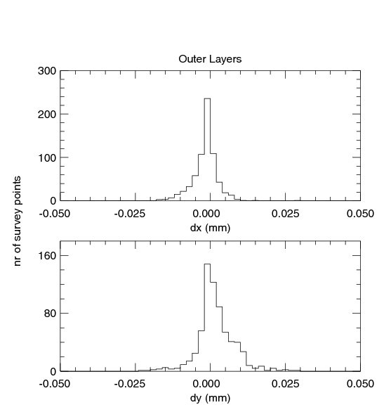
The position of the ladders and wheels in the overall support tube was determined by the placement of a ceramic ball in a ceramic cylinder. The requirements were precision, but after assembly the position was measured on a 3D survey machine with a precision of .
Figure 27 defines the coordinates of the ladder for the survey measurements after the modules were mounted on the ladder support. Figure 28 summarizes the results of the position measurements of the modules on the ladders. The differences between the measured values of the marker positions as compared to the nominal values are plotted. All points are within of the nominal position.
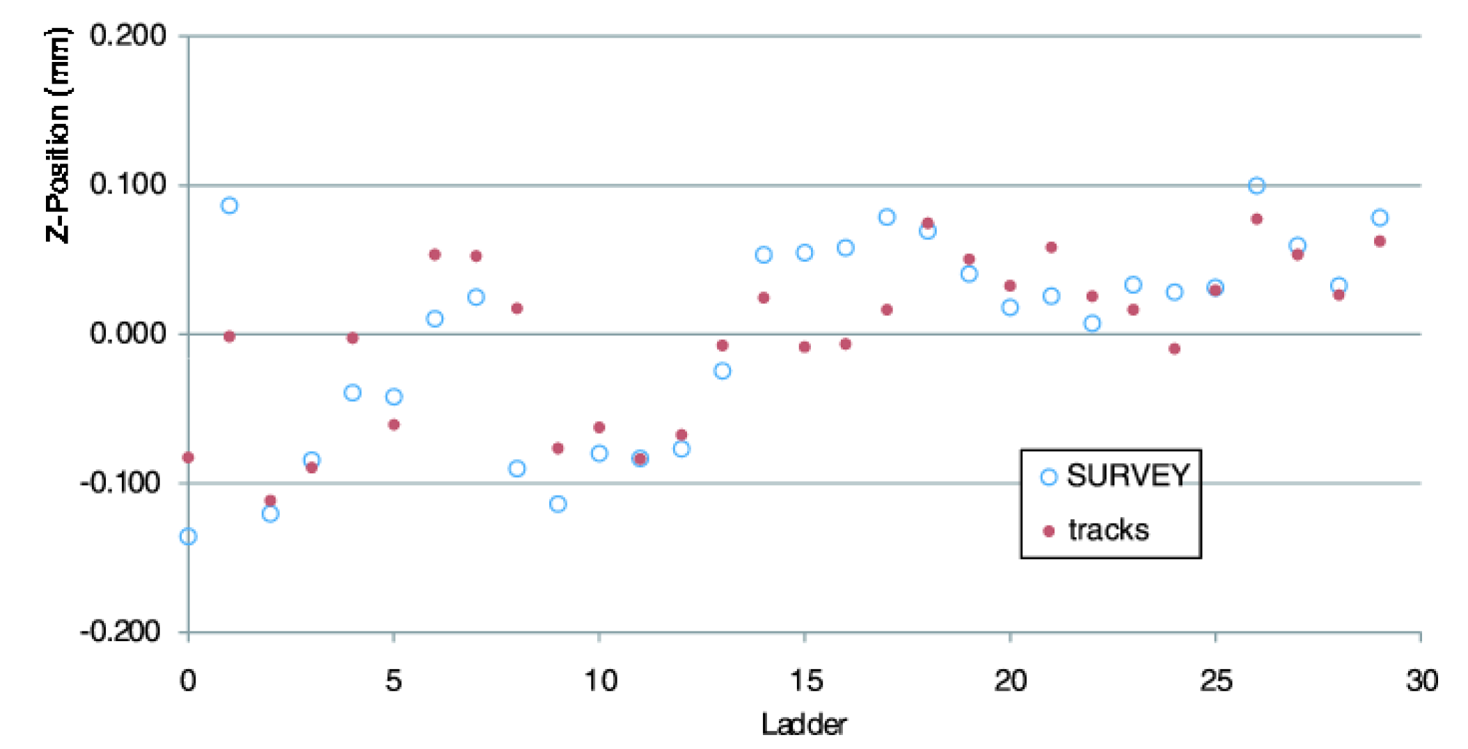
The -position of each ladder was surveyed after they were mounted in the overall support cylinder. The results are compared with cosmic ray measurements made prior to the installation in the experiment. Figure 29 shows that the mounting was precise within .
9.2.2 Laser Alignment
The laser alignment system consists of four straightness monitors placed around the perimeter of the MVD support tube. Each straightness monitor consists of a collimated laser beam, approximately parallel to the collider beam line, with seven semi-transparent silicon sensors positioned along its path, as shown schematically in Figure 30. Two of the sensors, mounted on the forward and rear CTD end-plates (positions 7 and 0), define the line for that laser beam. The five remaining sensors are mounted within the MVD at the forward and rear end-flanges, the forward and rear barrel flanges and the support structure for wheel 3. The alignment system is sensitive to motion of the support structure in directions perpendicular to the beam line. Full details of the system and its performance are given in [44].
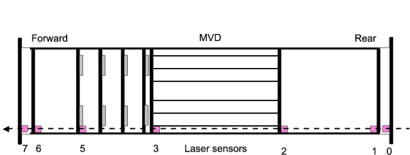
The laser alignment system measures the residuals at the five sensor positions along each of the four operational laser lines. A residual is defined as the distance between the measured laser beam position and the expected position based on a straight line defined by the two sensors attached to the CTD. Two residuals are measured in orthogonal directions in the plane of the sensor surface in a local coordinate system. The most useful information is obtained if a sequence of laser runs is taken over a long period, with the laser powered continuously and the beam controlled by a mechanical shutter. Using this procedure it has been possible to investigate whether, and by how much, the MVD support structure might move when environmental conditions change. The most important of these concern the HERA machine magnets nearest the ZEUS interaction point and the MVD on-detector electronics. The MVD is supported from the ZEUS CTD and the support structure has no direct mechanical connection to the beampipe. However all the service and readout cables - all exiting from the rear of the detector - are wrapped very tightly around the final magnet (GG) of HERA. This is a superconducting magnet that lies inside the beam-hole of the ZEUS RCAL (rear calorimeter) and was installed as part of the HERA-II upgrade programme. The space between the magnet and the RCAL modules is very limited, which is why the cables have to be very tightly bound to the magnet. It is known from position sensors on the magnet that it moves slightly when the magnet current is turned on or off. Thus it is possible that such movement could be transmitted to the MVD, though it is by no means obvious what type of movement of the MVD might result.
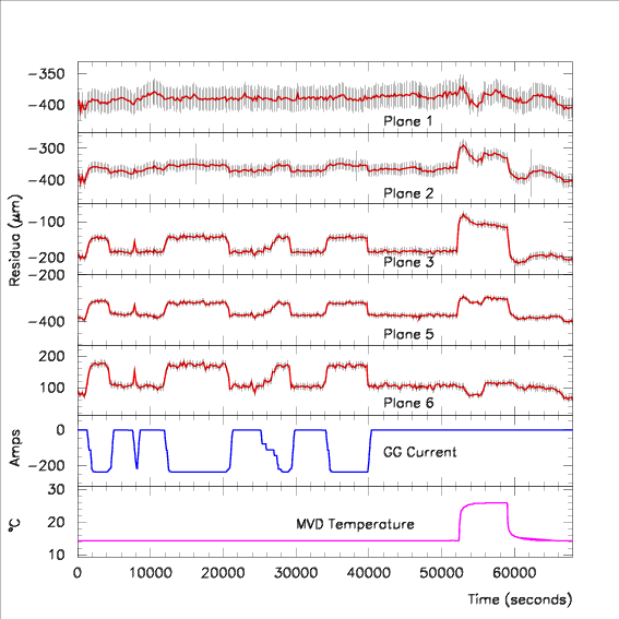
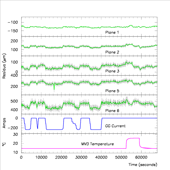
Figure 31 shows the residuals for sensor local- coordinates (left plots) and local- (right plots) for the five sensors within the MVD along laser-beam 2 as functions of time. The lowest two traces show the magnet current and the MVD temperature (measured at a position near wheel 3) for the same period. Considering the magnet current first, between times of 0 and 45000 there is a clear correlation in time between the mean residual values themselves and with the magnet current being zero or non-zero. There is also a tendency for the size of the movement to increase with increasing plane number. Such a pattern of movement is consistent with the MVD support tube being tilted about a fulcrum near the rear CTD support point by the movement transmitted from the GG magnet by the cables. Similarly, for times between 50000 and 65000, there is a correlation between sensor position and temperature. The change in temperature occurs when the MVD electronics is switched on or off. The pattern of movement is different in detail, the biggest effects are now seen in the three sensor planes nearest to the on-detector electronics – at planes 2, 3 and 5 (MVD barrel flanges and wheel 3).
The residual plots show that the position of a sensor is stable while the external effect is not changing and that the two positions of stability are themselves stable and reproducible. This has been investigated in more detail by averaging the residuals for periods of stability taken from long laser runs [44]. The results show that the difference in position locally can be as large as m, but that any hysteresis effects are at a level of m or less.
 |
 |
A long set of laser runs has been taken during a period of physics ‘luminosity’ running, when all environmental conditions should be stable - with both the GG magnet and the MVD electronics powered. The results show that the sensor position is stable to within an RMS of better than m over a period of 7 hours. It should be emphasised that all the measurements made with the laser system are of relative positions.
From these studies the following conclusions may be drawn:
-
•
The MVD support structure is very stable and there is no indication of any long term movement or step changes in position;
-
•
When external conditions vary, particularly the GG magnet on or off and the MVD on-detector electronics being powered or not, the MVD support structure shows movements locally as large as m;
-
•
Once the conditions return to the previous state the MVD returns to its previous position, to within m.
From these results it is clear that track data for precision alignment should be collected under the operational conditions of a ‘luminosity run’.
9.2.3 Alignment with Cosmics
For the bulk of tracks from lepton-proton collisions in the MVD only six 2-dimensional measurements are available. Therefore alignment of the detector with these tracks using MVD information alone is difficult. One way to overcome this problem is to use tracks from cosmic muons that traverse both halves of the detector. These typically provide twelve measurements in a very clean environment, but the method is limited by the fact that only small samples of cosmic muon tracks are available and that certain regions of the detector, particularly in the horizontal plane, are only poorly illuminated. In order to obtain a reasonable number of tracks, data samples recorded at different times during the first year of operation were combined. This is possible since the data from the laser alignment system indicate the position of the detector as a whole to be stable relative to the global ZEUS coordinate system with a precision of approximately . Thus, this method provides a robust initial determination of the alignment parameters of the detector. A detailed description of the method used and of the results can be found in [45]
An iterative two step method was used both to determine the global displacement of the entire MVD relative to the global ZEUS coordinate system as well as to align MVD ladders relative to each other. Statistics were not sufficient to perform an alignment of individual half modules with the cosmics data. In the first step well measured tracks were refitted after removing individual hits. In the second step the residuals of the “removed” hits were used in a least-squares fit in order to determine translational and angular alignment parameters. For the global alignment 6 free parameters, namely 3 translations and three angles, were used in the fit. For the local alignment a total of 180 parameters were used, namely the positions and angles of the 30 ladders in the barrel part of the detector. The global alignment was iterated 10 times, followed by 5 iterations of the local alignment. The whole procedure was then repeated. The method converged quickly and terminated after two global and three local iteration steps. The alignment with cosmics was not used to align the forward part of the MVD due to lack of coverage.
It should be noted that with this method track and alignment parameters are fitted independently of each other thus neglecting any correlations between them. Nevertheless, the method yields good robust results.
This can be seen in Fig. 32 which shows (a) the mean and (b) the width of track residuals for tracks from cosmic muons for the thirty ladders in the BMVD after applying the alignment procedure. These numbers can be considered as figures of merit for the cosmic alignment: The means are smaller than and the widths are about and for the and sensors respectively.
9.2.4 Alignment with tracks from ep Collisions
The final alignment was done using tracks from electron-proton collisions. While cosmic muon events have very clean signatures that lend themselves ideally for alignment purposes, they do not illuminate the full phase space, and are ultimately limited by statistics. The best alignment with cosmics can be expected for the barrel modules in the upper and lower parts of the detector, while the sideways barrel sensors are already less accessible to alignment with cosmic muons. The forward MVD is entirely inaccessible with this kind of alignment.
The largest sample of tracks for alignment is available from regular ep collisions. With 150 million events recorded in a good HERA-II year, such tracks are available in abundance even under very restricted selections, and they illuminate all detectors to the same degree as they are used for physics. Another advantage is that these alignment tracks are taken under identical conditions as for physics runs.
In comparison to cosmic muons, tracks from ep collision tracks start in the middle of the detector, hence in the barrel they traverse typically only six measurement layers of silicon, which leads to three hits in and three hits in sensors, though higher or smaller numbers of hits are possible depending on the trajectory. The transverse track parameters curvature, azimuth angle and impact parameter can obviously not be overconstrained by three MVD hits. To improve the constraints on the trajectory, two additional pieces of information are included:
-
•
the parameters of the CTD segment of the track helps to pin down the momentum of the track.
-
•
the run-by-run beam spot gives an additional constraint near the middle of the MVD.
Due to the relatively small number of MVD hits on collision tracks, it would not make sense to compute an unbiased residual by refitting the track with the hit of the layer in question excluded, as it is done in the alignment procedure for cosmic muons. Therefore, the residuals of a hit will be biased by the fact that hit coordinate and track parameters are correlated. This will not diminish the amount of information reflected in the hit residual, but the alignment procedure must take this correlation into account. It is therefore necessary to perform a global fit of all alignment parameters and all tracks in the alignment sample simultaneously. Since the aim is the individual determination of the positions and rotation angles of 600 barrel sensors with about 1 million tracks, this fit contains a large number of free parameters: about 3000 alignment parameters and several million track parameters. A specialized engine for this kind of fit is available called Millepede algorithm [46]. We have used it within the collision-based alignment.
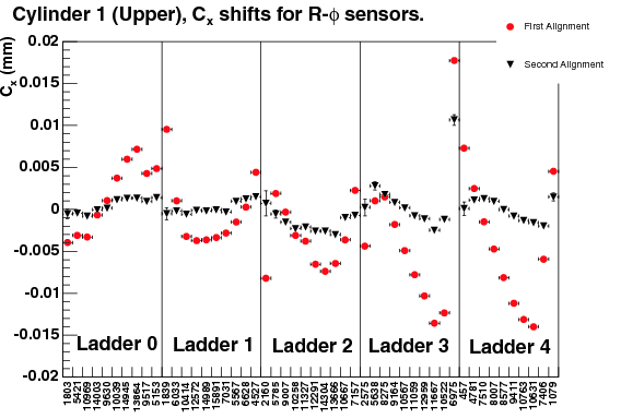
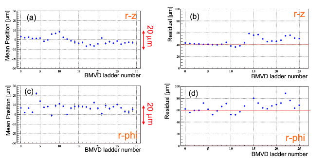
A small subset of the resulting constants is shown in Figure 33. The resulting shifts in the measurement direction of the sensor, , for the sensors of the five ladders in the middle cylinder in the upper half of the MVD are displayed. Within each of these ladders, the sensors are displayed in the order of their position along the proton beam direction. Most error bars are smaller than the symbol size, but one should be aware that the millepede fit does not account for multiple scattering, and hence the real errors will be larger. The alignment parameters range typically between . The strong correlation of neighboring sensors certifies to the high accuracy of the MVD assembly and the microscopic survey within each ladder. The dominantly linear variations of alignment parameters within the ladders indicate rotation around an axis normal to the ladder plane. The rotation angles are small (mrad) and become visible only due to the large leverage; they may reflect both adjustments of the ladder positions within the MVD frame, as well as a global rotation of the MVD relative to the nominal beam line. For some ladders the alignment constants show a non-linear pattern, one may speculate that their origin stems from a subtle deformation of the ladder, or from a warp-like buckling of the sensors.
9.2.5 Testing alignment performance
After implementing the alignment parameters in the MVD geometry, the consistency of the alignment procedure has been tested by reprocessing the track reconstruction with the updated geometry, and repeating the alignment procedure on the reprocessed sample. This second pass would also indicate a possible need for iteration, which might arise in case pattern recognition has been seriously suffering from initial misalignment. The result of the second alignment pass is shown by the triangular symbols in Figure 33. Since the resulting constants are close to zero, one concludes that the alignment procedure is self-consistent, and iteration is not necessary. The remaining variance of the points indicates a typical internal alignment accuracy of approximately in measurement direction.
 |
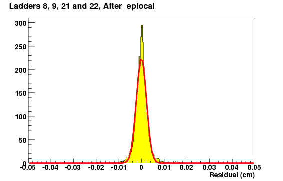 |
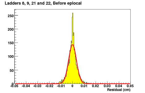
The improvement of the track quality by the alignment step is directly reflected in the distribution of the residuals. In Figure 34, the residual distributions for hits in the four ladders near are shown before and after alignment with collision tracks. The fitted width is found to improve considerably from to .
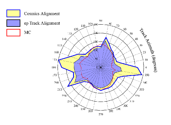
It is very important to find means of monitoring the track quality beyond simple residuals, and ideally they should be independent of the vertex reconstruction algorithm since the latter introduces an additional selection bias. A very useful observable is the impact parameter of high transverse momentum tracks with respect to the beam spot. The vast majority of high tracks in collisions at HERA are produced at the interaction point, within experimental resolution. The visible impact parameter distribution is therefore characterized by a narrow peak centered around zero, while decay particles from long-lived states only appear as a shallow background. The fitted width of the peak thus reflects the track resolution including effects from residual misalignment, plus a contribution from the beam spot width.
The fitted width of the visible impact parameter as a function of azimuth angle is shown in fig. 35, for tracks with . The coordinates of the beam spot have been determined by averaging primary vertex positions at run level. At the level of alignment with cosmic muons, the resolution is already close to the MC expectation in much of the upper and lower areas of the barrel, while it is relatively poor – up to – in the azimuth range between 160∘ and 210∘, and between 350∘ and 0∘. This effect is not very surprising, since these regions are expected to be least covered by the cosmic muon sample. The alignment with tracks from collisions is found to improve the impact parameter resolution in all azimuth regions, and the improvement is particularly large in the problematic areas.
9.3 Tracking efficiency
The tracking efficiency is a quantity that depends not only on details of the detector but to a significant degree on details of hit and track reconstruction, such as clustering algorithms, track pattern recognition, the track fit, the alignment of the detector and many other parameters. Here we give only a simple estimation of this quantity which indicates that the tracking efficiency is indeed high. For this purpose Figure 36 shows the percentage of tracks found in the CTD that have either at least 2 or at least 4 associated hits in the MVD as a function of the azimutal angle.
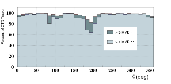
This quantity approximately measures the MVD efficiency folded with that of the track pattern recognition. Impurity in the CTD hit selection causes a slight underestimate while impurity in the MVD cluster selection causes a slight overestimate. Overall the efficiency is flat at a level in excess of as a function of the polar angle with three characteristic dips near , and . These dips are due on the one hand to holes in the geometrical acceptance of the detector and to an accumulation of bad channels. In particular these are two small holes in the coverage of the inner cylinder near and , the presence of only two cylinders near and an accumulation of bad channels around .
9.4 Specific energy loss
The analog detector electronics provides a 10-bit value of the observed pulse height which is related to the specific energy loss of particles traversing the sensitive volume of the detector. These values calibrated to one for a pure sample of pions, e. g. from the decay of neutral kaons, are shown in Figure 37. One can easily identify the three different bands stemming from protons, kaons and pions. The resolution is around % varying slightly with momentum and particle species.
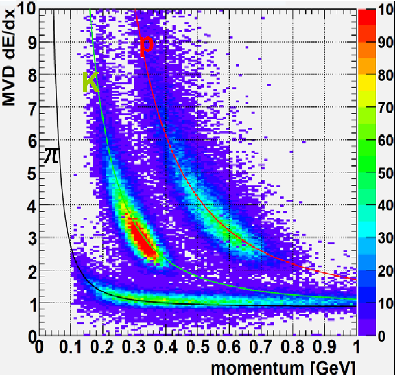
9.5 Impact on physics signals
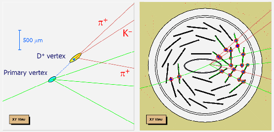
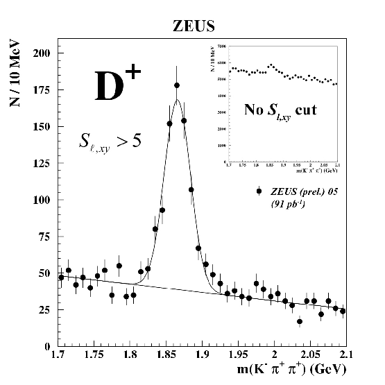
The improved track reconstruction and accuracy of the MVD has enabled the experiment to use impact parameter and decay length signatures in heavy flavor analysis. One example is the reconstruction of the meson in its decay channel . The MVD allows detection of this decay pattern routinely as a displaced secondary vertex, as illustrated in the event display in Figure 38. For each accepted candidate, the decay length in the plane transverse to the beam, , has been calculated as
| (2) |
where and are the components of the transverse momentum of the , and are its vertex coordinates, and and are the transverse coordinates of the beam spot. The decay length significance has been computed as , where the error takes the resolutions of tracks and beam spot into account. Fig. 39 shows the resulting invariant mass spectrum for and GeV, for DIS events collected in the run between December 2004 and September 2005, corresponding to an integrated luminosity of . The mass spectrum shows a very clean signal of mesons with very little background, thanks to the suppression of tracks from the primary interaction. The data sample has been used to determine the mean lifetime of the with an accurary of 10% [47] in agreement with the world average. This illustrates the flavor-tagging capabilities of the ZEUS Micro-Vertex Detector.
10 Summary and Conclusions
In this article we have described the design, construction and performance of the Microvertex Detector built for the ZEUS experiment at the HERA collider at DESY. In this final section we briefly review key design choices and other decisions taken during the construction of the detector and comment on how the detector has performed as a consequence of these.
A silicon strip detector was installed in the ZEUS experiment at the HERA collider at DESY in 2001 and by the end of the HERA running in 2007 an integrated luminosity of pb-1 with 99% reliable MVD data was recorded. An impact parameter resolution of m has been achieved reaching design specifications.
A 60 cm long barrel with three concentric silicon layers surrounds the interaction point with layers at radii of approximately 4, 9 and 12 cm. In the forward proton direction four wheels are mounted perpendicular to the beamline. The total silicon surface amounts to m2.
The readout pitch is m with 5 intermediate strips enhancing the charge division. In a readout module two sensors are joined using a Upilex cable with copper strips and then connected to the analog HELIX3.2 chip. In a testbeam a spatial resolution of m s been measured for perpendicular tracks on a single sensor. For a half module a resolution of m was measured.
Lightweight carbon fiber structures support the sensors, together with the readout chips and required water cooling and cabling; the average amount of material is 3% of a radiation length per layer for perpendicular incidence.
The signal-to-noise has been stable over the five years of data taking. The number of dead channels slowly increased to 5%. The origin is not quite certain but there is some suspicion about the stability of the connection of the hybrids with the readout chips to the sensor and readout cable.
A radiation monitor system was installed since the silicon sensors as well as the Helix chip are radiation sensitive components. The radiation hardness requirement was a total dose of kGy, four times the expected dose. Three types of monitors were used: pin diodes, thermoluminescent dosimeters and radiation field effect transistors. The worst case estimate is a dose of a few kGy after 6 years of operation resulting in a degradation of the signalnoise limited to 10% for a few sensors at the inner cylinder of the barrel.
During construction the positions of the sensors on a ladder were carefully checked and archived with optical survey measurements. Small deviations from design (m) were found and therefore none of these measurements were used during reconstruction. Tracks from cosmic muons provide the alignment of the ladders inside the overall frame. A laser alignment system monitors the stability of the vertex detector. When the nearby superconducting low beta magnets were switched on, deformations of the order of m were observed. Under stable running conditions it is however shown that the geometry is stable within m. At present the alignment accuracy is below m using tracks from collisions.
Kalman filter techniques are used for track fitting as well as vertex finding. Apart from a region in where only two layers of silicon are traversed the impact parameter resolution has reached the design value of m for high momentum tracks.
11 Acknowledgments
The authors would like to acknowledge the work and dedication of many people who made this project possible. Not all can be mentioned here. However, the many contributions of technicians and engineers from the collaborating institutes, namely F. Benotto, H. Boer Rookhuizen, H. Botschig, P. de Groen, T. Handford, J. Hauschildt, J. Hill, M. Jaspers, R. Kluit, H. Kok, M. Kraan, K. Kretschmer, J. Kuyt, B. Payne, U. Pein, A. Rietmeiyer A. Speck, O. Strangfeld, P. P. Trapani, P. Verlaat and A. Zampieri are highly appreciated.
References
- [1]
- [2] ZEUS Coll., U. Holm (ed.); The ZEUS Detector; Status Report; DESY (1993); unpubl.; available on [http://www-zeus.desy.de/bluebook/bluebook.html].
- [3] ZEUS Coll., M. Derrick et al., A Measurement of at ; Phys. Lett.B 293, 465-477 (1992).
- [4] D. Dannheim et al., Design and tests of the silicon sensors for the ZEUS micro vertex detector; Nucl. Instrum. Methods A 505, 663-682 (2003) [hep-ex/0212026].
- [5] UPILEX is polyimide film. UPILEX is a registered trademark of UBE Industries LTD., Japan. [http://www.upilex.jp/eindex.html].
-
[6]
M. Feuerstack-Raible; Overview of microstrip readout chips;
Nucl. Instrum. Methods A 447, 35-43 (2000).
W. Fallot-Burghardt et al.; Helix128-2.x User Manual; HD-ASIC-33-0697. Modifications for ZEUS (HELIX 3.2):[http://www.asic.kip.uni-heidelberg.de/ trunk/projects/Helix/]. - [7] U. Kötz et al., Silicon Strip Detectors with Capacitive Charge Division; Nucl. Instrum. Methods A 235, 481-487 (1985).
- [8] M. Milite; The Internal Structure of Charmed Jets in Photoproduction at HERA and Tests of the ZEUS Microvertex Silicon Sensor; PhD Thesis, University of Hamburg (2001) DESY-THESIS-2001-050.
- [9] M. Moritz; Measurement of the High Neutral Current DIS Cross Section at HERA; PhD Thesis, University of Hamburg (2002) DESY-THESIS-2002-009.
- [10] L. A. T. Bauerdick et al.; Beam test of silicon strip sensors for the ZEUS micro vertex detector; Nucl. Instrum. Methods A 501, 340-358 (2003)
- [11] V. Chiochia; Measurement of Beauty Quark Production in Deep Inelastic Scattering at HERA; PhD Thesis, University of Hamburg (2003) DESY-THESIS-2003-031.
- [12] J. Martens; Simulationen und Qualitätssicherung der Siliziumstreifendetektoren des ZEUS-Mikrovertex detektors; MSc Thesis, University of Hamburg (1999) DESY-THESIS-1999-044.
- [13] Hamamatsu Photonics K.K., Japan [http://www.hamamatsu.com/] .
- [14] Austria Mikrosysteme GmbH; Schloss Premstatten, 8141 Unterpremstatten, Austria.
- [15] U. Trunk, Development and Characterisation of the Radiation tolerant Helix 128-2 Readout Chip for the HERA-B Microstrip Detector, PhD Thesis, Heidelberg (2000).
- [16] AXON’ S.A.S., Route de Chalons-en-Champagne, 51210 Montmirail, France.
- [17] T. Fusayasu et al.; Analog readout modules for the ZEUS Microvertex detector; Nucl. Instrum. Methods A 436, 281-284 (1999)
- [18] M. D. M. de Fez Laso et al.; Proceedings of 2nd Workshop on Electronics for LHC Experiments; Balatonf red, Hungary (1996).
- [19] [http://www.hep.ucl.ac.uk/zeus/mvd/candc.html]
- [20] [http://www-zeus.desy.de/components/mvd]
- [21] Cirlex is a laminated Kapton film. Both Cirlex and Kapton are registered trademarks of DuPont [http://cirlex.com].
- [22] A. Polini; The architecture of the ZEUS Micro Vertex Detector DAQ and second level global track trigger; CHEP-2003-MOGT005 (2003).
- [23] C. Youngman; The ZEUS Data Acquisition System; Proc. of CHEP92, Annecy (1992).
- [24] C. Youngman et al., The Design and Performance of the ZEUS Global Track Trigger, acc. for pub. by Nucl. Instrum. Methods A.
- [25] A. Polini, M. Sutton, S. Topp-Jorgensen; The CTD-MVD Global-Tracking-Trigger Interface; ZEUS Note 99-034 (1999); unpubl.
- [26] A. Polini; UVMElib: an easy approach to the VMEbus for Motorola PPC boards with Universe bridge and Lynx-OS; ZEUS Note 99-071 (1999); unpubl.
- [27] A. Polini, M. Pwalam, C. Youngman; A multipurpose VME interrupt and service board for the ZEUS MVD detector; ZEUS Note 03-009 (2003); unpubl.
- [28] ESD Electronic Hannover, Germany, [http://www.esd.electronics.com].
- [29] iseg Spezialelektronik Gmbh, Bautzner Landstraße 23, D-01454 Radeberg/OT Rossendorf, Germany, [http://www.iseg-hv.com].
- [30] ZEUS Collab., M. Derrick et al.;The ZEUS Leading Proton Spectrometer and its Use in the Measurement of Elastic Photoproduction at HERA; Z. Phys C73, 253-268 (1997) [hep-ex/9609003].
- [31] A. Mastroberardino; Azimuthal asimmetries in Diffractive Deep Inelastic Scattering and the Low Voltage System of the ZEUS Microvertex Detector; Tesi di Dottorato, Universitá della Calabria (2002).
-
[32]
NIKHEF, Amsterdam, Holland, [http://www.nikhef.nl/pub/departments/ct/po
/doc/SPICAN.pdf]. -
[33]
[http://www.nikhef.nl/pub/departments/mt/
projects/zeus/vertex/website.html]. - [34] [http://www.frenzel-berg.de/].
- [35] EMS, Sonnenhang 3, D-85304 Iimmuenster, [http://www.ems-wuensche.com/].
- [36] I. Bloch et al.; A radiation Monitor for the ZEUS Detector at HERA; IEEE Trans. Nuclear Science 51, 1606-1612 (2004).
- [37] D. Dannheim; Search for events with isolated leptons and large missing transverse momentum in collisions at HERA; PhD Thesis, University of Hamburg (2003) DESY-THESIS-2003-025.
- [38] J. J. Velthuis; Radiation hardness of the ZEUS MVD frontendchip and Strangeness production in scattering at HERA; PhD Thesis, University of Amsterdam, (2003).
- [39] SINTEF Electronics and Cybernetics, [http://www.ittf.no].
- [40] T. I. Meyer; PIN photodiodes for radiation monitoring and protection in the BaBar silicon vertex tracker; Int. J. Mod. Phys. A16S1C, 1084-1086 (2001) [hep-ex/0010058].
-
[41]
NMRC, Ireland;
[ http://www.nmrc.ie/projects/radfets/index.html]. - [42] E. Maddox; Study of heavy quark production at HERA using the ZEUS microvertex detector; PhD Thesis, University of Amsterdam (2004).
- [43] T. Matsushita et al.; Optical Alignment System for the ZEUS Micro Vertex Detector Nucl. Instrum. Methods A 466, 383-389 (2001).
-
[44]
K. Korcsak-Gorzo et al.; The Optical Alignment System of the
ZEUS MVD; acc. for pub. by Nucl. Instrum. Methods A.
[doi:10.1016/j.nima.2007.06.046] -
[45]
T. Kohno; Alignment of the ZEUS micro-vertex detector using cosmic tracks;
Nucl. Instrum. Methods A 559, 153-157 (2006). - [46] V. Blobel, Software alignment for tracking detectors; Nucl. Instrum. Methods A 566, 5-13 (2006).
- [47] ZEUS Collaboration, Measurement of the D+ Lifetime with the ZEUS Micro-Vertex Detector at HERA-II, submitted to XXXIII International Conference on High Energy Physics, Moscow (2006), available on [ http://www-zeus.desy.de/physics/phch/conf/ichep06/ hfl/9/ZEUS-prel-06-016.ps].