Present Address: ]Low Temperature Laboratory, Helsinki University of Technology, PO Box 3500, 02015 TKK, Finland
The effect of screening long-range Coulomb interactions on the metallic behavior in two-dimensional hole systems
Abstract
We have developed a technique utilizing a double quantum well heterostructure that allows us to study the effect of a nearby ground-plane on the metallic behavior in a GaAs two-dimensional hole system (2DHS) in a single sample and measurement cool-down, thereby maintaining a constant disorder potential. In contrast to recent measurements of the effect of ground-plane screening of the long-range Coulomb interaction in the insulating regime, we find surprisingly little effect on the metallic behavior when we change the distance between the 2DHS and the nearby ground-plane.
pacs:
71.30.+h, 72.20.-i, 73.21.FgThe ground state of a 2D electron or hole system is determined by the ratio of the inter-particle Coulomb energy to the kinetic energy, with the regimes , , and corresponding to the gas, liquid and solid phases of the 2D system. Recently, much effort has gone into studying the phase diagram of 2D systems, focussing on the role of interactions and disorder Abrahams01 . An interesting approach is to use an adjacent metallic ground-plane to screen the long-range Coulomb interactions, and thereby study how the length-scale of the Coulomb interactions controls the ground state of the 2D system. Ground-plane screening was used to probe the effect of Coulomb interactions in the melting of the Wigner crystal state of electrons on liquid helium Jiang88 ; Mistura97 . More recently, Huang et al. Huang06 have used a nearby ground-plane to study the insulating state in an ultra-low density 2D hole system (2DHS), and find that the insulating behaviour is strongly affected by screening the Coulomb interaction. It would be interesting to perform a corresponding study for the metallic behavior observed in a dilute 2DHS. However, this presents a significant technical challenge because on one hand, the higher hole density in the metallic regime requires that the distance between the ground-plane and the 2DHS be quite small ( nm) to achieve effective screening, and on the other, 2DHSs of sufficient quality to observe the metallic behavior are typically buried deep ( nm) in the semiconductor.
In this paper, we report a study of the influence of ground-plane screening on the metallic behavior in a 2DHS. We find that screening the long-range Coulomb interactions has a relatively small effect in the metallic regime, in contrast to the insulating behavior Huang06 . Our findings suggest that hole-hole screening within the 2DHS already significantly reduces long-range Coulomb interactions in the metallic regime, consistent with the view that the metallic behavior arises due to temperature-dependent screening of the Coulomb interactions between holes and charged impurities Gold90 ; DasSarma00 ; Zala01 . To overcome the technical challenge of studying the ground-plane screening in the metallic regime, we have used a heterostructure featuring two quantum wells buried nm beneath the semiconductor surface and separated by only nm, such that the 2DHS in the upper quantum well acts as the nearby ground-plane for the 2DHS in the lower quantum well. Using a metal surface-gate, we can deplete the upper 2DHS, making the surface-gate become the ground-plane, and thus increasing the distance to the ground-plane by a factor of . This is a major advantage as can be changed in a single device and measurement cool-down, thereby keeping the disorder relatively constant, unlike previous studies.
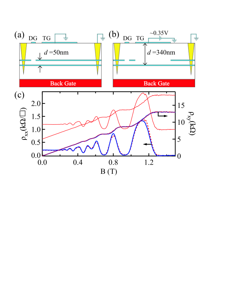
Our approach is illustrated in Fig. 1(a/b), and utilizes a double quantum well (DQW) structure featuring a doped semiconductor back-gate, an overall top-gate (TG) and a set of depletion gates (DG) adjacent to each AuBe ohmic contact. The top and back gates allow the hole densities in the two 2DHSs to be controlled. The ohmic contacts connect to both QWs and the depletion gate is used to sever all connections to the upper 2DHS with the exception of the drain contact, via which the upper 2DHS is grounded (see Fig. 1(a)). Hence current passes only via the lower 2DHS. In this experiment, we measure the temperature dependent resistivity of the lower 2DHS when it is separated from a nearby ground plane by nm (Fig. 1(a)) and nm (Fig. 1(b)). For the nm case, the top-gate is set to 0 V, resulting in a 2DHS with a density of approximately cm-2 in the upper QW, which acts as a ground plane. For the nm case, the top gate is set to V, depleting the upper 2DHS in regions directly beneath the top gate. Despite being positively biased, the top-gate is still an equipotential, and hence acts as a ground-plane when the upper 2DHS is depleted. Combining this operating principle with appropriate adjustments to the various gate biases, we can switch between the two values while keeping the density in the lower 2DHS constant, and repeat the experiment at different densities.
The device is fabricated on a (311)A AlGaAs/GaAs DQW heterostructure, featuring two 20nm GaAs QWs separated by a 30nm thick Al0.3Ga0.7As barrier that ensures there is no tunneling between the two 2DHSs ( K). The heavily-doped (311)A substrate acts as the back-gate and is separated by 3 m from the lower QW. The device is fabricated into a Hall bar structure oriented along the high-mobility direction. Transport measurements were performed in a Kelvinox 100 dilution refrigerator, with a 20 mK base temperature. Standard four-terminal low-frequency a.c lock-in techniques were used with a constant excitation voltage of 20 V applied at Hz.
In Fig. 1(c) we present magnetotransport measurements in the two device configurations presented in Fig. 1 (a/b) to demonstrate that we can maintain a constant in the lower 2DHS while changing the ground-plane distance from 50 nm (dashed red trace) to 340 nm (solid blue trace). Due to the close overlap of these two traces, we have reproduced the 50 nm traces and offset them vertically for clarity (solid red lines). The Hall slope ( - right axis) and the period of the Shubnikov-de Haas (SdH) oscillations ( - left axis) show that the density remains constant to within despite changing by a factor of 7.
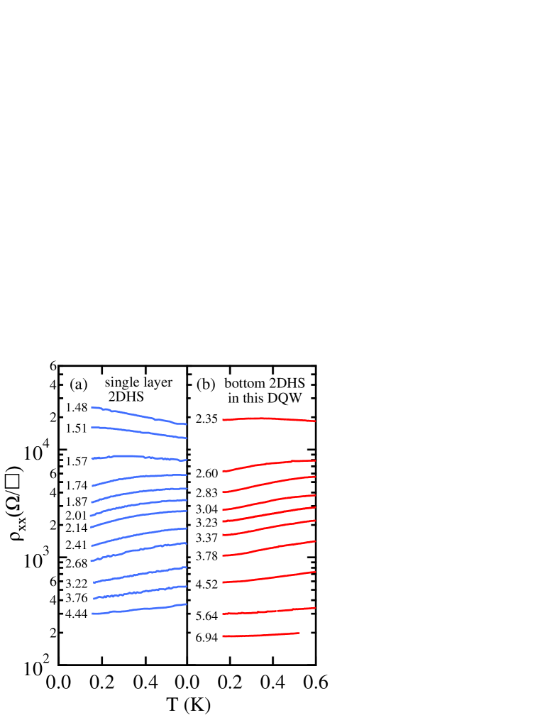
We commence our study by comparing the temperature dependent resistivity measured for nm with that obtained in a prior study using a similar p-GaAs heterostructure containing a single QW Hamilton01 . This allows us to confirm that the depleted upper 2DHS in our device does not significantly alter the results obtained for large . In Fig. 2(a) we show data obtained in Hamilton01 , where a clear metal-insulator transition is observed. Insulating behavior () is observed at low densities, with a transition to metallic behavior () occurring at cm-2. With further increases in , the metallic behavior weakens again, as expected because the hole-hole interactions weaken with increasing . Very similar behavior is obtained in our device for nm, as shown in Fig. 2(b). At high densities, weak metallic behavior is observed, which becomes stronger as is decreased. We are unable to measure in the insulating regime because our device becomes unstable when the top-gate bias is too high, however this is not an impediment to the experiments presented here.
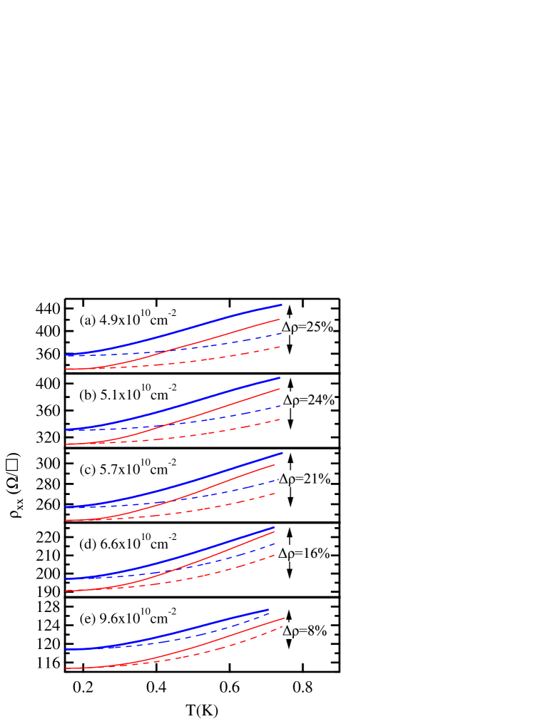
In Fig. 3 we present measured with nm (thick lines) and nm (thin lines) at five different densities deep in the metallic regime. Moving down through the panels in Fig. 3, the metallic behavior weakens with increasing , as indicated by the percentage change in resistivity over the measured temperature range. The most obvious effect of reducing to 50 nm is to offset to a lower resistivity, likely caused by the upper 2DHS screening the lower 2DHS from the long-range impurity scattering from the upper modulation doping layer.
The resistivity is predominantly composed of three parts: a temperature-independent Drude contribution due to impurity scattering, and two temperature-dependent contributions due to phonon scattering and hole-hole interactions. We calculate using Karpus’ theory Karpus90 , as done previously for 2D hole systems Prosku02 ; Yasin05 . The Drude contribution is then obtained by extrapolating to . The calculated phonon contributions for each and are presented as dashed lines in Fig. 3. At the highest density, where interactions are weakest, is a remarkably good fit to the measured considering there are no fitting parameters, giving confidence in our application of Ref. Karpus90, to calculating the phonon contribution. In contrast, at lower densities, there is a significant temperature dependence that cannot be described by phonon scattering alone, which we attribute to hole-hole interactions (screening).
Following Proskuryakov et al., we isolate the contribution of the Coulomb interactions to the conductivity by subtracting the phonon and Drude contributions using Prosku02 . In Fig. 4 (a), we plot vs corresponding to the nm trace in Fig. 3(a), and find an approximately linear dependence of on , with a negative slope corresponding to metallic behavior. It is common to interpret such data using the theory of Zala et al. Zala01 to obtain the Fermi liquid interaction parameter . This is normally achieved by fitting vs in the linear regime (i.e., , where is the Fermi temperature) to obtain the normalized slope , which is related to by Noh03 . However, recent studies have shown that the theory of Zala et al. Zala01 , which assumes a short-range scattering potential, does not extract the correct values of for modulation-doped samples where long-range scattering from remote ionized impurities is significant Clarke07 . Hence in this paper, we focus on the slope as a measure of the strength of the metallic behavior, henceforth called the ‘metallicity’, and simply note that if we fit Zala’s theory to our data, we obtain values similar to those previously obtained in modulation-doped GaAs 2D hole systems by Proskuryakov et al. Prosku02 .
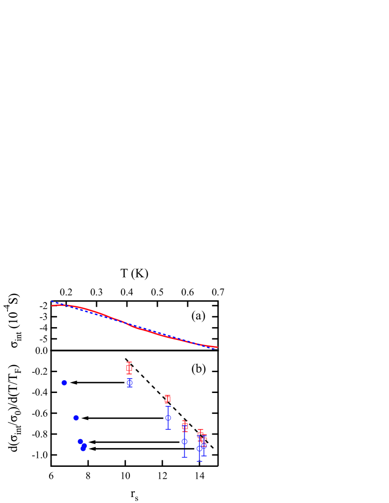
We now directly analyze the effect of changing the ground-plane separation , and thus the length-scale of the Coulomb interactions, on the metallic behavior. To do this, we obtain the metallicity for each trace in Fig. 3 by taking a linear fit to the corresponding vs data (Fig. 4(a)). We limit our fitting to the range mK K. The lower limit is the minimum hole temperature in our experiment (obtained following McPhail04 ) whilst the upper limit ensures that . The relative strength of the hole-hole Coulomb interactions is characterized by , which in the absence of a nearby ground-plane, takes the form , where is the dielectric constant. In Fig. 4(b), we plot the metallicity as a function of for nm (open squares) and nm (open circles). In each case is negative, indicating metallic behavior. As Fig. 4(b) shows, there is little change in the metallicity as is reduced from 340 nm to 50 nm at constant density, but the metallic behavior weakens with increasing density (i.e., decreasing ), as expected. The presence of the ground-plane introduces negative image-charges that cause the holes to interact as though they were dipoles rather than single positive charges, resulting in a Coulomb potential that falls off as instead of for Huang06 . This leads to an additional term in that accounts for the Coulomb interaction between the hole’s image-charge and another hole in the 2DHS, giving Widom88 ; Ho08 :
The additional term in Eqn (1) reduces the effective as becomes comparable to the hole-hole separation Huang06 , with ranging from nm for the data in Fig. 3. Thus, whilst for nm the effective reduction in is quite small (), it is quite substantial for nm, as demonstrated in Fig. 4(b), where we have re-plotted the metallicity for nm vs. (solid circles).
We now consider the effect of the ground plane on the metallicity. The dashed line in Fig. 4(b) shows the metallicity of the unscreened nm data tends to decrease as is reduced. If the metallicity depends only on , for example, if it is due to long-range Coulomb interactions Zala01 , then when the effective is decreased by reducing from 340 nm to 50 nm, the metallicity should also be reduced. When plotted against , the metallicity for the nm data (solid circles) should lie in the upper left corner of Fig. 4(b), not down in the lower left of the figure. In fact rather than being reduced, the nm metallicity is actually slightly greater than for nm, suggesting that the ground-plane has almost no effect on the metallic behavior. This is in contrast to recent experiments on the screening of long-range Coulomb interactions in the insulating regime Huang06 , where single layer 2DHS samples with 250, 500 and 600 nm were examined. The hopping conductivity was fitted to the form , and the exponent , which is related to the strength of the insulating behavior, was found to be very sensitive to d, and uniquely determined by the ratio , which was changed from 1.1 to 5 [4]. In our experiment, changes by almost an order of magnitude, from 2 to 19, yet we find that the metallicity is primarily determined by alone.
One possible explanation for the contrasting behaviour is that in the metallic regime the long-range Coulomb interactions are already screened by the other holes in the 2DHS, significantly diminishing the effect of the ground-plane. In the insulating regime, this screening by other holes is much weaker, giving the ground-plane significant effect. This is consistent with recent studies of the compressibility of 2D systems Allison06 , which found that the Thomas-Fermi screening radius increases by over an order of magnitude when going from the metallic to insulating regime.
We finish with some final comments on the experiment. First, it is particularly interesting to note that our findings are consistent with the metallic behavior being due to the temperature-dependent screening of the hole-impurity Coulomb interactions Gold90 ; DasSarma00 ; Zala01 . Second, because the screening layer for nm is a nearby 2DHS, we have estimated the possible contribution of Coulomb drag to , since this can be a significant effect in DQW structures Pillar05 . Due to the relatively large QW spacing and high densities, we calculate the drag contribution to to be in our device. Finally, in addition to theoretical calculations Ho08 , we have performed experiments to check that the upper 2DHS density is sufficient to act as a proper screening layer. We find no change in the metallic behavior when the upper 2DHS density is varied Ho07 , confirming that the upper 2DHS acts as an effective ground-plane.
This work was funded by Australian Research Council (ARC) and the EPSRC. L.H.H. acknowledges support from the UNSW and the CSIRO. O.K. acknowledges support from the UNSW. M.Y.S, A.R.H, A.P.M. and R.D. acknowledge support from the ARC. We thank O.P. Sushkov for helpful discussions and J. Cochrane for technical support.
References
- (1) :
- (2) B.L. Altshuler, D.L. Maslov and V.M. Pudalov, Physica E 9, 2, (2001); S. V. Kravchenko and M. P. Sarachik, Rep. Prog. Phys., 67, 1, (2004)
- (3) H.-W. Jiang and A. J. Dahm, Surf. Sci. 196, 1 (1988).
- (4) G. Mistura, T. Günzler, S. Neser, and P. Leiderer, Phys. Rev. B 56, 8360 (1997).
- (5) J. Huang, D. S. Novikov, D. C. Tsui, L. N. Pfeiffer and K. W. West, Cond-mat/0610320.
- (6) A.Gold, Phys. Rev. B 41, 8537 (1990).
- (7) S. Das Sarma and E.H. Hwang, Phys. Rev. B 61, R7838 (2000).
- (8) G. Zala, B. N. Narozhny, and I.L. Aleiner, Phys. Rev. B 64, 214204 (2001).
- (9) A. R. Hamilton, M. Y. Simmons, M. Pepper, E. H. Linfield, and D. A. Ritchie, Phys. Rev. Lett. 87, 126802 (2001).
- (10) Y. Y. Proskuryakov, A. K. Savchenko, S. S. Safonov, M. Pepper, M. Y. Simmons, and D. A. Ritchie, Phys. Rev. Lett. 89, 076406 (2002).
- (11) V. Karpus, Semicond. Sci. Tech. 5, 691 (1990).
- (12) C. E. Yasin, T. L. Sobey, A. P. Micolich, A. R. Hamilton, M. Y. Simmons, W. R. Clarke, L. N. Pfeiffer, K. W. West, E. H. Linfield, M. Pepper, and D. A. Ritchie, Phys. Rev. B 72, 241310(R) (2005).
- (13) H. Noh, M. P. Lilly, D. C. Tsui, J. A. Simmons, E. H. Hwang, S. Das Sarma, L. N. Pfeiffer, and K. W. West, Phys. Rev. B 68, 165308 (2003).
- (14) W. R. Clarke, C. E. Yasin, A. R. Hamilton, A. P. Micolich, M. Y. Simmons, K. Muraki, Y, Hirayama, M. Pepper and D. A. Ritchie, Nature Physics 4, 55 (2008).
- (15) S. McPhail, C.E. Yasin, A.R. Hamilton, M.Y. Simmons, E.H. Linfield, M. Pepper and D.A. Ritchie, Phys. Rev. B 70, 245311 (2004).
- (16) A. Widom and R. Tao, Phys. Rev. B 38, 10787 (1988).
- (17) O.P. Sushkov (Private Communication); calculations showing that the 2DHS produces almost exactly the same effect as a metal gate will be published elsewhere.
- (18) R. Pillarisetty, H. Noh, E. Tutuc, E. P. De Poortere, K. Lai, D. C. Tsui and M. Shayegan, Phys. Rev. B 71, 115307 (2005).
- (19) G. Allison, E. A. Galaktionov, A. K. Savchenko, S. S. Safonov, M. M. Fogler, M. Y. Simmons, and D. A. Ritchie, Phys. Rev. Lett. 96, 216407 (2006).
- (20) L.H. Ho, W.R. Clarke, R. Danneau, O. Klochan, A.P. Micolich, M.Y. Simmons, A.R. Hamilton, M. Pepper and D.A. Ritchie, Physica E 40, 1700 (2008)