Threshold voltage and space charge in organic transistors
Abstract
We investigate rubrene single-crystal field-effect transistors, whose stability and reproducibility are sufficient to measure systematically the shift in threshold voltage as a function of channel length and source-drain voltage. The shift is due to space-charge transferred from the contacts, and can be modeled quantitatively without free fitting parameters, using Poisson’s equation, and by assuming that the density of states in rubrene is that of a conventional inorganic semiconductor. Our results demonstrate the consistency, at the quantitative level, of a variety of recent experiments on rubrene crystals, and show how the use of FET measurements can enable the determination of microscopic parameters (e.g., the effective mass of charge carriers).
Organic single-crystal field-effect transistors (FETs) are opening new possibilities for the detailed investigation of the intrinsic electronic properties of organic semiconductors and of their interfaces deBoer04 ; Gershenson06 . Transistors where a single-crystal was suspended on top of a gate electrode, have led to the observation of intrinsic transport properties, such as mobility anisotropy Sundar04 and metallic-like temperature dependence Podzorov04 . Current work is aiming at the systematic study of microscopic electronic processes in these systems. Examples are the study of polaronic effects at the interface between organic crystals and highly polarizable dielectrics Stassen04 ; Hulea06 ; Fratini08 , the analysis of band-like transport at interfaces with low- materials Podzorov05 ; Pernstich08 , and the detailed investigation of electronic transport at metal/organic interfaces Molinari08 . In most cases, a quantitative analysis of the data in terms of well-defined microscopic models has been possible, but the consistency of results obtained in different experiments remains to be verified.
Virtually all experiments on single crystal FETs have focused on transport through a well-formed conducting channel, i.e. in the regime when the gate voltage is biased well above the threshold voltage . Here, we use rubrene single-crystal FETs for a systematic experimental investigation of the behavior of the threshold voltage itself. Specifically, we have measured the electrical characteristics of short channel transistors as a function of channel length , and extracted the dependence of on and on source-drain bias . We find that systematically shifts to more positive values when is decreased or is increased, a behavior originating from changes in the space-charge transferred from the contacts into the semiconductor. We model the system using Poisson’s equation, under the assumption that the density of states in the molecular crystals has the same functional dependence as in inorganic semiconductors, and find excellent quantitative agreement between experimental data and calculations, without introducing any adjustable parameter. Our results indicate that the effective mass of carriers in the rubrene valence band is close to the free electron mass, provide information about the low-energy density of states, and show that the physical picture used to interpret a variety of recent experiments Molinari08 ; Li07 is internally consistent at a quantitative level.
Not much is currently known about the microscopic processes determining the behavior of the threshold voltage in organic transistors. Work done on thin-film devices has established that this behavior can be complex, exhibiting large sample-to-sample fluctuations and instabilities VGStress . These phenomena have so far prevented systematic experiments, and are posing severe technological problems. The situation appears to be different in single-crystal devices, with recent work showing considerably better reproducibility Reese09 .
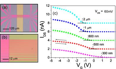
The fabrication of the rubrene FETs relies on the lamination of thin ( -thick) single-crystals on top of a highly doped silicon substrate (acting as a gate) covered with 500 nm SiO2, with predefined oxidized copper electrodes deBoer03 . The devices are identical to those that we used previously for the investigation of the contact resistance, and are therefore very well characterized Molinari08 ; Molinari07 . In that work we focused on the high-gate voltage regime with a fully formed channel; here we analyze the behavior of the threshold voltage .
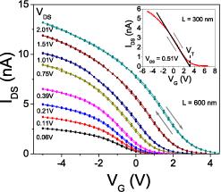
Transport measurements were performed at room temperature, in the dark and in vacuum ( mbar), using a HP4156A parameter analyzer. Owing to the short channel length, the resistance of the devices is dominated by the contacts, resulting in the characteristic (sub-linear) shape Molinari08 of the transfer curves seen in Figs. 1 and 2. Special care was taken in restricting the applied gate voltage to the narrowest possible range around , to suppress possible effects of bias stress. Accordingly, the output characteristics of our devices are hysteresis-free, with stable and reproducible values. To extract these values, we have used the linear extrapolation method and fitted the linear regime of the transfer curve that follows the onset of conduction (as illustrated in the inset of Fig. 2). The uncertainty on the values extracted using this method is at most 0.1 V (for the shortest devices), and usually better.
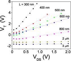
The behavior of the threshold voltage as a function of channel length and bias is apparent from Figs. 1c and 2. Fig. 1c shows the transfer characteristics of transistors with different channel lengths, measured at a same value of . It is apparent that systematically shifts to more positive values in devices with a shorter channel. Fig. 2 shows measurements done on an individual transistor for increasing values of . A shift of to positive values (see Fig. 3) is clearly present, which is found to be larger for shorter devices. These trends resemble those recently reported in Ref. Reese09 . Fig. 3 provides a complete overview of the behavior of in our experiments. The different devices (i.e., sets of FETs with different channel length fabricated on a same crystal) investigated, exhibited identical trends and similar magnitude of the observed effects.
The shift of as a function of and originates from the transfer of charge from the source and drain contacts into the semiconductor. At low (i.e., ), charge transfer occurs to align the Fermi level in the metal and in the bulk of the semiconductor. As the contact separation is decreased, the corresponding charge density in the (bulk) region of the semiconductor between source and drain contact increases. At finite , additional charge is transferred from the contacts to the semiconductor due to capacitive coupling, similarly to what happens in space-charge limited current measurements SCLC . As charge density and potential are linked by Poisson’s equation, the transferred charge induces a shift in electrostatic potential, which needs to be compensated by a shift in the threshold voltage to switch off conduction. In simpler terms, to switch off conduction, the space charge transferred from the electrodes into the bulk of the semiconductor needs to be compensated by an equal and opposite amount of charge accumulated in the channel (i.e., by a shift in ).
At a quantitative level we consider the case of low-bias first, and we calculate the profile of charge density transferred from the electrodes into the bulk of the semiconductor (Fig. 4a) by solving Poisson equation. To this end we employ a one-dimensional (1D) model, to describe how electrostatic potential and charge density vary in the bulk of the semiconductor, away from an interface with a metal contact (Fig. 4b). We then have
| (1) |
Here , with the effective mass of holes in the ”highest occupied molecular orbital” (HOMO) band of rubrene (i.e., the valence band of the organic semiconductor), is the vacuum permittivity and the relative dielectric constant of rubrene. The last equality assumes that the density of states in rubrene has the same dependence as in a conventional one-band semiconductor, i.e. parabolic dispersion relation with effective mass , which allows expressing the local density of charge carriers as a function of the local potential As&Me . Clearly, the validity of this hypothesis needs to be checked by comparing the results of the calculations to the experimental data.
There are two boundary conditions associated to Poisson’s equation. The first, = , fixes the constant in the potential so that corresponds to the local distance between the Fermi level and the valence band edge in the semiconductor ( is the energy difference between the metal Fermi level and the valence band edge; when a large gate voltage is applied corresponds to the height of the Schottky barrier present at the metal/semiconductor interface). The second is , which imposes that the electric field vanishes in the bulk of the semiconductor, far away from the interface with the metal. Under these conditions, the solution to Poisson’s equation is
| (2) |
and the corresponding charge carrier density is given by
| (3) |
Note that in Eq. 1 we have neglected ”bulk” contributions to the charge density, e.g. due to (unintentionally present) dopants or thermally activated charge carriers. Accordingly, equations 2 and 3 are valid inside the semiconductor, only at a small distance from the electrode surface, where the charge transferred from the contacts is larger than the one present due to dopants, which in high-purity crystals is Kaji09 . This value is much smaller than what is usually found in organic semiconductors, and hence in our devices the space charge penetrates deeper into the rubrene crystals. Using Eq. 3, with Molinari08 (see discussion below) and taking into account the overlapping of the space charge regions coming from both contacts, it is easy to verify that the charge transferred from the contacts is larger than even for devices with (normally, due to the large doping in organic semiconductors, this length is only a few tenths of nanometers Worne08 ).
To link the calculated quantities to the data, we impose that the total amount of space charge transferred from the contacts into the bulk region of the semiconductor between source and drain contacts is compensated, at threshold, by an equal and opposite amount of charge accumulated in the channel (i.e., by a shift in threshold voltage ). We then get
| (4) |
where is the spatial average of the carrier density present in the overlapping space-charge regions originating from the two contacts, is the gate capacitance per unit area, and is the thickness of the rubrene crystal (measured with a profilometer). This estimate of is approximate, in that our calculation does not take into account the precise geometry. For our devices, we estimate that the error is a geometrical factor of the order of unity (see the below discussion on the dependence of ).
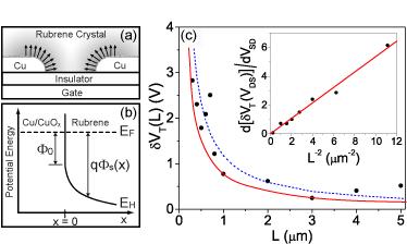
Fig. 4c shows the comparison between the predictions of equation 4 and the measured values (where is the average threshold voltage obtained from devices with 10 L 50 ; all measurements were performed at ). The lines represent the results of the calculations using the values of for a CuOx/rubrene interface, known from our study of the contact resistance: typically varies between and in different devices Molinari08 . For the hole effective mass , we take the value extracted from recent optical spectroscopy experiments, which is close to the free electron mass Li07 . All other quantities in the theoretical expression are known, and there are no free adjustable parameters. As it is apparent from Fig. 4c, the quantitative agreement between calculations and experimental data is remarkably good.
This result has several important implications. First, the comparison shown in Fig. 4c relies on parameters extracted from completely different experiments, such as measurements of contact resistance and infrared spectroscopy. Therefore, the agreement found in our analysis of indicates that our description of the electronic properties of rubrene is internally consistent at a quantitative level. Second, our result indicates that describing the low energy density of states in the valence band of rubrene in terms of the ”textbook” expression for conventional inorganic semiconductors is a good approximation. Third, and more in general, this work shows how ”simple” measurements of FET electrical characteristics can be used to extract microscopic parameters—e.g., the carrier effective mass—that are not otherwise easily accessible experimentally.
The analysis of the threshold voltage behavior as a function of source-drain bias confirms that the shift in is due to space charge injected from the contact into the semiconductor. In this case we estimate the amount of charge injected into the semiconductor as , where is the capacitance between the injecting electrode and the rubrene crystal (this concept is identical to that used in the description of space-charge limited current curves SCLC ). By reasoning analogously to the case of the -dependence, we then obtain
| (5) |
Where for the capacitance between contact and crystal, we have taken as a very simple approximation the expression of a parallel plate capacitance.
Equation 5 predicts that the shift of threshold voltage is linear in source-drain voltage, which is the case for (see Fig. 3), and that the slope of this linear relation should scale with the separation between source and drain as , as found experimentally (see inset of Fig. 4c). From the linear relation between and we extract the value of which is comparable to that obtained by directly measuring the crystal thickness (deviations of a factor of are found in different samples, as can be expected given the crude estimates of the capacitances).
Note that all the effects that we have investigated here scale inversely to the gate capacitance (see Eq. 4 and 5). This is a typical signature of the so-called short-channel effects, which are well-known in silicon devices MOSFETSMODELS . What is remarkable in our organic transistors is that, owing to the low doping concentration, these effects dominate already at a fairly large channel length (), i.e. length scales which are typical of devices used in practical applications Gelinck04 .
In summary, rubrene single-crystal FETs are sufficiently stable and reproducible to perform systematic investigations of threshold voltage shift. From the length dependence of this shift, we have extracted information about the microscopic properties of rubrene, such as density of states and a quantitative estimate for the effective mass in the valence band. In conjunction with a variety of earlier experiments—infrared spectroscopy, and quantitative studies of bias and temperature-dependent contact resistance—our results show that our current picture for the understanding of organic semiconductors does account for many experimental observations in a way that is internally consistent at a quantitative level.
We gratefully acknowledge A. S. Molinari for help with the experiments. AFM also gratefully acknowledges financial support from the Dutch NWO-VICI program and from the Swiss NCCR MaNEP.
References
- (1) R.W.I. de Boeret al., Phys. Status Solidi A 201, 1302 (2004).
- (2) M. E. Gershenson et al., Rev. Mod. Phys. 78, 973 (2006).
- (3) V. C. Sundar et al., Science 303, 1644 (2004).
- (4) V. Podzorov et al., Phys. Rev. Lett. 93, 086602 (2004).
- (5) A. F. Stassen et al., Appl. Phys. Lett. 85, 3899 (2004).
- (6) I. N. Hulea et al., Nat. Mater. 5, 982 (2006).
- (7) S. Fratini et al., New J. Phys. 10, 033031 (2008).
- (8) V. Podzorov et al., Phys. Rev. Lett. 95, 226601 (2005).
- (9) K. P. Pernstich et al., Nat. Mater. 7, 321 (2008).
- (10) A. S. Molinari et al., Appl. Phys. Lett. 92, 133303 (2008).
- (11) Z. Q. Li et al., Phys. Rev. Lett. 99, 016403 (2007).
- (12) M. Matters et al., Synth. Met. 102, 998 (1999); H. L. Gomes et al., Appl. Phys. Lett. 84, 3184 (2004); T. Richards and H. Sirringhaus, Appl. Phys. Lett. 92, 023512 (2008);
- (13) C. Reese and Z. Bao, Adv. Funct. Mater. 19, 763 (2009).
- (14) R.W.I. de Boer et al., Appl. Phys. Lett. 83, 4345 (2003).
- (15) A. S. Molinari et al., Appl. Phys. Lett. 90, 212103 (2007).
- (16) A. Lampert and P. Mark, Current Injection in Solids, (Academic Press, New York, 1970).
- (17) N. W. Ashcroft and N. D. Mermin, Solid State Physics (Sounders College, Philadelphia, 1976), Chapter 28.
- (18) In reference Molinari08 , we demonstrate that the energy level alignment at a Cu/CuOx/rubrene interface essentially follows the Schottky-Mott limit. This is due to the presence of the CuOx tunnel barrier, which causes a weak coupling between the metal and molecules, resulting in a small density of interfacial states (5 1011 - 1 1012 ).
- (19) T. Kaji et al., to be published in Adv. Mater.
- (20) J. H. Worne et al., Nano Res. 1, 341 (2008).
- (21) N. Arora, MOSFET Models for VLSI Circuit Simulation, Theory and Practice (Springer-Verlag, Austria, 1993), Chapter 5.
- (22) G. H. Gelinck et al., Nat. Mater. 3, 106 (2004).